This simple MOSFET controlled transformerless power supply circuit can be used for delivering a continuously variable 0 to 300V DC output and a current control from 100 mA to 1 Amp.

To protect against my high voltage research projects from going up in smoke permanently, I developed an easy circuit which is able to render a variable voltage supply of 0 to 330 Volt.
But please be cautioned, the circuit is not isolated from mains potential, and therefore can inflict a lethal shock.
The supply is short-circuit proof: the current is restricted to approximately 100mA.
WARNING: ALL THE ABOVE CIRCUITS CARRY LETHAL MAINS VOLTAGE AND THEREFORE ARE EXTREMELY DANGEROUS. IT CAN KILL ANYBODY, IF TOUCHED ANYWHERE ON THE CIRCUIT IN POWERED CONDITION. OBSERVE APPROPRIATE PRECAUTIONS TO AVOID ANY MISHAP.
Circuit Operation
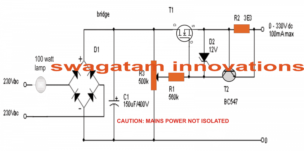
The design does not require a transformer, rather a 100 watt bulb is introduced at the input in order to provide ultimate safety in case of a short circuit or a component failure.
The mains voltage from after passing through the lamp is rectified with bridge D1 (1Amp / 500V) and C1.
T1 is configured as a source follower: the source of T1 complies with the voltage of the wiper of R3. D2 is insured to safeguard the gate of T1.
T2 and shunt resistor R2 establish the current limiter. Whenever the output current results in being excessive, T2 quickly discharges the gate of T1.
This stops the current from increasing any further. The value of R3 was basically identified experimentally; however it actually depends on the Hfe of T2 which means you may need to adjust the value of R2 appropriately.
Keep in mind T1 requires a large heatsink: in nastiest situation T1 would probably disperse 330V x 100mA = 33Watt!
You may try mosfets such as a BUZ 326 (400V/10.5Amp) or you may likewise use an IRF740 (400V/10Amp).
The output impedance of the power supply varies according to the beta of T1, therefore the bigger the MOSFET, the lesser the output impedance!
Circuit Diagram
UPDATE:
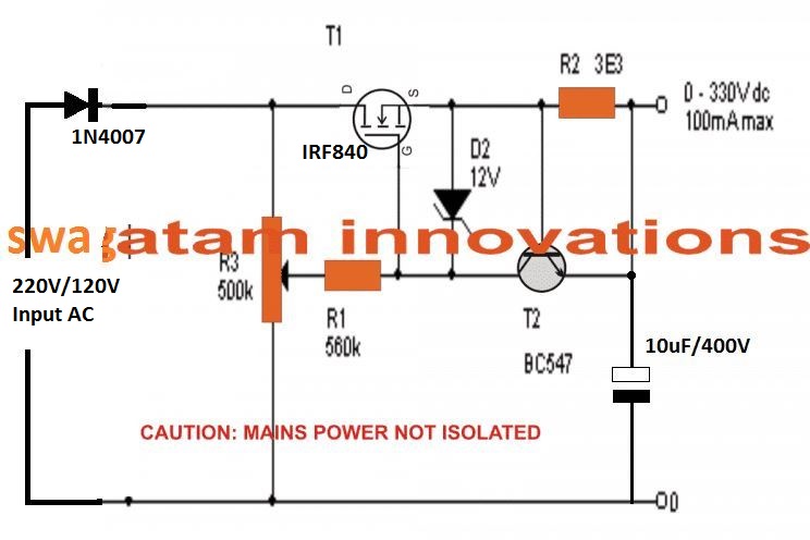
The above design could be much simplified as indicated in the following diagram. The bridge rectifier has been eliminated which drastically reduces the stress level on the MOSFET.
However, the ripple generated due to a half wave rectification may be significantly higher.
The output 10uF filter capacitor helps to reduce this to some extent. The value of this capacitor could be increased to higher levels for improving the DC quality.
The input series lamp can be added, although this may not be required due to the presence of the current control stage in the design. However, for better safety a fuse may be added in series with the input line.
The output load specification must not exceed 100 ma
Video Proof:
This power supply can be used to obtain a regulated power output, variable right from zero to 300 volts maximum. All the devices should be mounted on heatsinks.
Working Principle
The circuit regulates the output voltage using an IRF840 MOSFET (T1) as the main regulating element.
The 500k potentiometer (R3) controls the gate voltage of the IRF840 thus varying the output voltage.
The output current is controlled via the current-sensing resistor R2. When the voltage drop across R2 exceeds the base-emitter voltage of the BC547 transistor (T2 typically 0.6V to 0.7V) then T2 turns ON and reduces the gate voltage of T1 limiting the current.
D2 (12V Zener diode) ensures that the voltage of the IRF840 between its gate and source does not exceed 12V.
Key Parameters
- Vout: Adjustable output voltage (0–300V DC)
- Iout: Maximum output current (A)
- R2: Current sensing resistor (ohms)
- R3: Potentiometer for voltage control (ohms)
- Vin: Input voltage (rectified 220V AC ≈ 310V DC)
Formulas
- Output Voltage Control
The gate voltage of T1 is determined by the setting of the 500k potentiometer (R3). The output voltage is approximately proportional to the gate voltage of T1.
Vout ≈ Vgs(T1) - Vds(on)
- Where:
- Vgs(T1) = Gate-to-source voltage of T1
- Vds(on) = Drain-to-source voltage when T1 conducts (small value around few volts)
- Current Limiting (Iout)
The current limiting is handled by the sensing resistor R2. The voltage drop across R2 is compared with the base-emitter voltage of T2 (Vbe approximately 0.6V–0.7V). When the voltage drop across R2 exceeds Vbe, T2 turns ON and reduces the gate voltage of T1, thereby limiting the current.
Iout = Vbe / R2
- Where:
- Iout = Maximum output current (A)
- Vbe = Base-emitter voltage of T2 (typically 0.6V–0.7V)
- R2 = Current sensing resistor (ohms)
- Power Dissipation in R2
The sensing resistor R2 must dissipate power proportional to the output current:
P(R2) = Iout2 * R2
- Where:
- P(R2) = Power dissipated in R2 (W)
Choose a resistor with a power rating higher than P(R2) for safe operation.
- MOSFET Power Dissipation
The IRF840 MOSFET dissipates power due to the voltage drop across it and the output current:
P(T1) = (Vin - Vout) * Iout
- Where:
- P(T1) = Power dissipated in T1 (W)
- Vin = Input voltage (DC, ≈310V for rectified 220V AC)
- Vout = Output voltage (adjustable)
- Iout = Output current (A)
Ensure T1 has adequate heat sinking to handle the calculated power dissipation.
Example Calculations
Let us Assume:
Vin = 310V DC peak rectified from 220V AC.
Vout = 300V DC
Iout = 0.5A (desired maximum current)
Vbe = 0.6V
Step 1: Calculate R2 (Current Sensing Resistor)
R2 = Vbe / Iout = 0.6 / 0.5 = 1.2 ohms
Step 2: Power Dissipation in R2
P(R2) = Iout2 * R2 = 0.52 * 1.2 = 0.3W
Choose a resistor with at least a 0.5W rating for safety.
Step 3: Power Dissipation in T1 (IRF840)
At maximum output:
P(T1) = (Vin - Vout) * Iout
= (310 - 300) * 0.5
= 10 * 0.5 = 5W
At lower output voltages the power dissipation in T1 will increase so choose the heat sink to handle the worst-case scenario.
A Failproof 300V Variable Power Supply Design
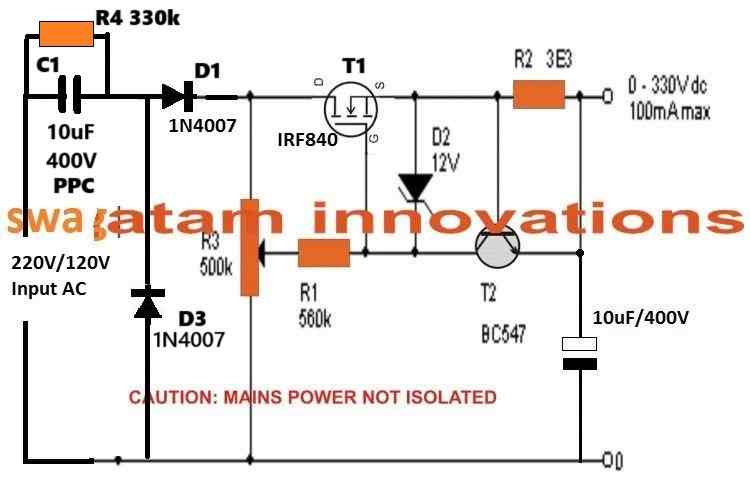
To make the above 300V adjustable power supply completely safe and failproof, you can modify it by adding an input current limiting capacitor, as shown in the following diagram.
However, please remember that the circuit is safe and failproof only for the MOSFET, but it still carries a floating 300V AC, which can be lethal for any human if the circuit is touched in open and powered condition.
Using a Combination of BJT and Mosfets
Circuit Operation
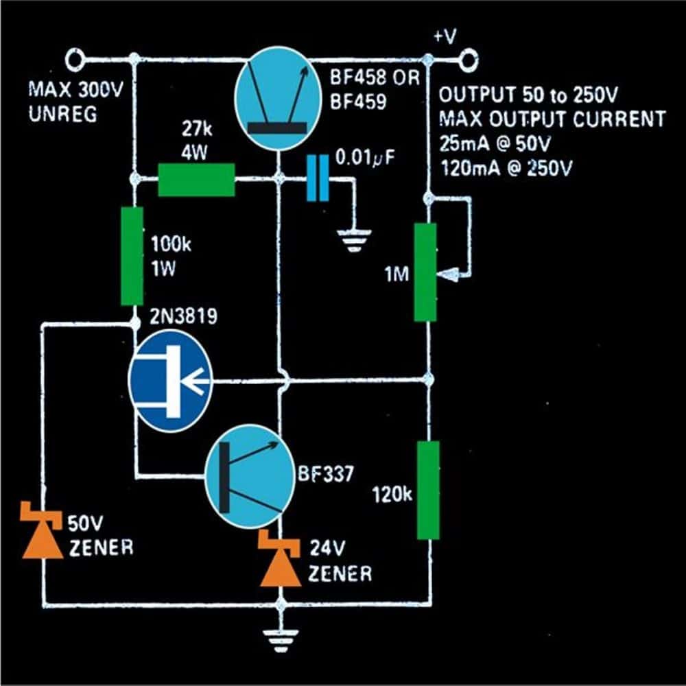
The next transformerless 0-300V variable power supply circuit diagram can be understood with the following points:
As can be seen in the figure, a high voltage transistor BF458 is used as the main load handling device.
Its base bias is controlled by another high voltage transistor BF337 whose emitter is clamped to a stable 24 volts.
An FET is used for selecting the base current of the transistor BF337 via a pot of 1M.
This setting adjusts the base current for the BF337 which in turn restricts the main transistor BF458s voltage and current flow to the output.
The input to the circuit may be derived directly from the mains AC after proper rectification and filtration using a bridge network and a 10u/400V capacitor.
The entire circuit is extremely dangerous to touch, due care should be maintained while making and testing this circuit.
Converting 80V DC to 5V DC Stabilized Output
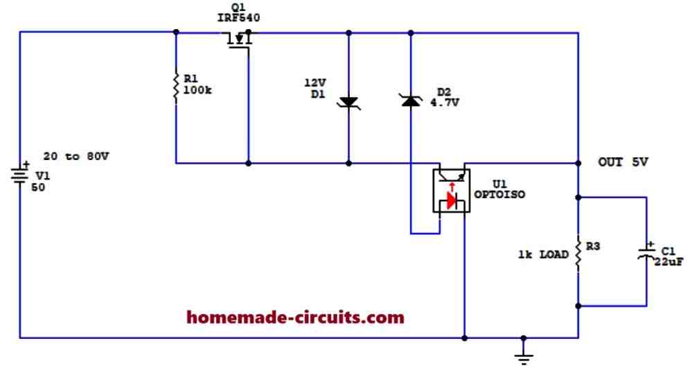
The above explained 300V MOSFET regulator circuit was successfully modified by Mr. Luigi to convert a varying input between 20V and 80V DC into a stabilized 5V DC output, using an opto-coupler feedback, as shown in the following figure. I am grateful to Mr. Luigi for contributing this design to this website.

Have Questions? Please Comment below to Solve your Queries! Comments must be Related to the above Topic!!