In this post I have explained how to make 2 accurate long duration timer circuits ranging from 4 hours to 40 hours, which can be upgraded further for getting even longer delays. The concepts are fully adjustable.
A timer in electronics is essentially a device which is used for producing time delay intervals for switching a connected load. The time delay is set externally by the user as per the requirement.
Introduction
Please remember that you can never produce long accurate delays using only a single 4060 IC or any CMOS IC.
I have confirmed practically that beyond 4 hours IC 4060 begins deviating from its accuracy range.
IC 555 as a delay timer is even worse, it's almost impossible to get accurate delays even for an hour from this IC.
This inaccuracy is mostly due to capacitor leakage current, and inefficient discharging of the capacitor.
ICs like 4060, IC 555, etc basically generate oscillations which are adjustable right from a few Hz to many Hz.
Unless these IC are integrated with another divider counter device such as IC 4017, getting very high accurate time intervals may not be feasible. For getting 24 hour, or even days and week intervals you will have integrate a divider/counter stage as shown below.
In the first circuit we see how two different modes of ICs can be coupled together to form an effective long duration timer circuit.
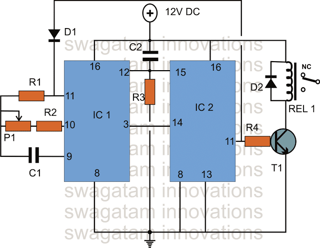
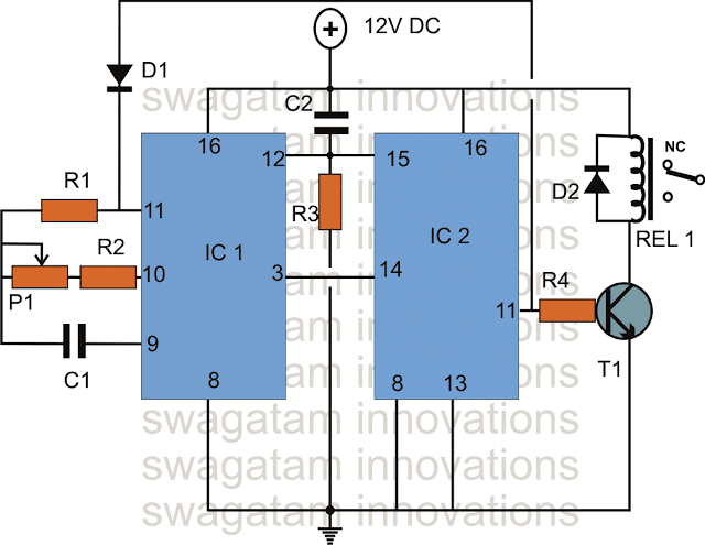
1) Circuit Description
Referring to the circuit diagram.
- IC1 is an oscillator counter IC consisting a built in oscillator stage and generates clock pulses with varying periods across its pins 1,2,3,4,5,6,7,9,13,14,15.
- The output from pin 3 produces the longest time interval and therefore we select this output for feeding the next stage.
- The pot P1 and the capacitor C1 of IC1 can be used for adjusting the time span at it pin 3.
- The higher the setting of the above components the longer the period at pin #3.
- The next stage consists of decade counter IC 4017 which does nothing but increase the time interval obtained from IC1 to ten folds. It means if the the time interval generated by IC1s pin #3 is 10 hours, the time generated at pin #11 of IC2 would be 10*10 = 100 hours.
- Similarly if the time generated at pin #3 of IC1 is 6 minutes, would mean a high output from pin#11 of IC1 after 60 minutes or 1 hour.
- When power is switched ON, capacitor C2 makes sure that the reset pins of both the ICs are appropriately reset, so that the ICs begin counting from zero rather than from some irrelevant intermediate figure.
- As long as the counting progresses, pin #11 of IC2 remains at logic low, such that the relay driver is held switched OFF.
- After the set timing lapses, pin#11 of IC2 goes high activating the transistor/relay stage and the subsequent load connected with the relay contacts.
- The diode D1 ensures that the output from pin#11 of IC2 locks the counting of IC1 by providing a feed back latch signal at its pin #11.
Thus the whole timer latches until the timer is switched OFF and restarted again for repeating the entire process.
Parts List
R1, R3 = 1M
R2, R4 = 12K,
C1, C2 = 1uF/25V,
D1, D2 = 1N4007,
IC1 = 4060,
IC2 = 4017,
T1 = BC547,
POT = 1M linear
RELAY = 12V SPDT
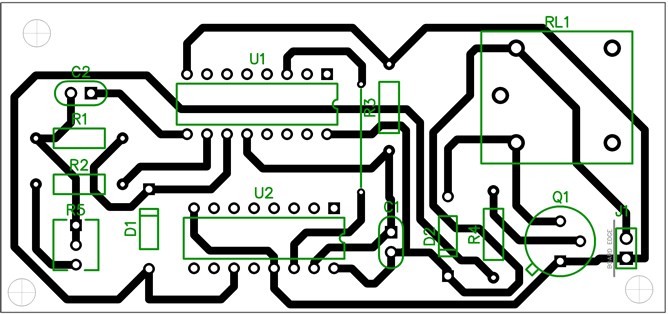
PCB Layout
Formula for Calculating Delay output for IC 4060
Delay Period = 2.2 Rt.Ct.2(N -1)
Frequency = 1 / 2.2 Rt.Ct
Rt = P1 + R2
Ct = C1
R1 = 10(P1+R2)
Adding Selector Switch and LEDs
The above design could be further enhanced with a selector switch and sequential LEDs, as indicated in the following diagram:
How it Works
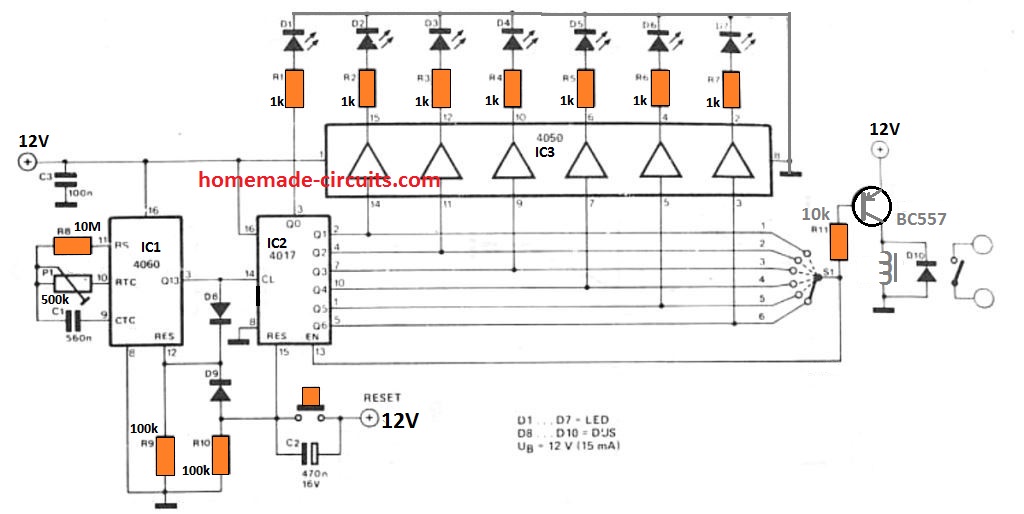
The main element of the timing circuit is a 4060 CMOS device, which is made up of an oscillator along with a 14 stage divider.
The frequency of the oscillator could be tweaked through potentiometer P1 in order that the output at Q13 is around a single pulse each hour.
The period of this clock beat could be extremely quick (around 100 ns), as it additionally resets the whole 4060 IC by way of diode D8.
The 'once each hour' clock pulse is given to the 2nd (divide-by-ten) counter, the 4017 IC. One of several outputs of this counter is going to be logic high (logic one) at any given instant.
When the 4017 is reset, output Q0 goes high. Right after one hour, output Q0 will turn low and output Q1 may become high, etc. Switch S1 as a result allows the user to choose a time interval through one to six hours.
When the chosen output becomes high, the transistor turns off and the relay gets switched OFF (thus turning off the connected load).
Once the enable input of the 4017 is furthermore attached to the wiper of S1 any succeeding clock pulses turns out to have no impact on ihe counter. The device will consequently continue to be in the switched OFF condition until the reset switch is presed by the user.
The 4050 CMOS buffer IC along with the 7 LEDs are incorporated to offer indication of the range of hours which may have essentially elapsed. These parts could, obviously, be removed in case an lapsed time display is not needed.
The source voltage for this circuit is not really crucial and could be cover anything from 5 and 15 V, The current usage of the circuit, excluding the relay, will be in the range of 15 mA.
It is advisable to pick a source voltage that may be matching the specifications of the relay, to ensure that any problems are avoided. The BC 557 transistor can handle a current of 70 mA, so make sure the relay coil voltage is rated withing this current range
2) Using Only BJTs
The next design explains a very long duration timer circuit which uses only a couple of transistors for the intended operations.
Long duration timer circuits normally involve ICs for the processing because executing long duration delays requires high precision and accuracy which is possible only using ICs.
Achieving High Accuracy Delays
Even our very own IC 555 becomes helpless and inaccurate when long duration delays are expected from it.
The encountered difficulty for sustaining high accuracy with long duration is basically the leakage voltage issue, and the inconsistent discharging of the capacitors which leads to wrong starting thresholds for the timer producing errors in the timing for each cycles.
The leakages and inconsistent discharge issues become proportionately bigger as the capacitor values get bigger which becomes imperative for obtaining long intervals.
Therefore making a long duration timers with ordinary BJTs could be almost impossible as these devices alone could be too basic and cannot be expected for such complex implementations.
So How can a Transistor Circuit Produce Long Accurate Duration Time Intervals?
The following transistor circuit handles the above discussed issues credibly and can be used for acquiring long duration timing with reasonably high accuracy (+/-2%).
It's simply due to effective discharging of the capacitor on every new cycle, this ensures that the circuit begins from zero, and enables accurate identical time periods for the selected RC network.
Circuit Diagram
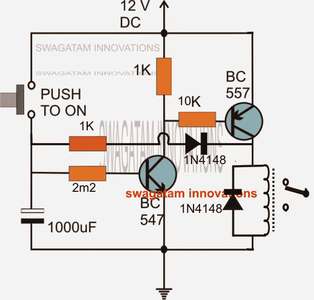
The circuit may be understood with the help of the following discussion:
How it Works
A momentary push of the push button charges the 1000uF capacitor fully and triggers the NPN BC547 transistor, sustaining the position even after the switch is released due to the slow discharging of the 1000uF via the 2M2 resistor and the emitter of the NPN.
Triggering of the BC547 also switches ON the PNP BC557 which in turns switches ON the relay and the connected load.
The above situation holds on as long as the 1000uF is not discharged below the cut off levels of the the two transistors.
The above discussed operations are quite basic and make an ordinary timer configuration which may be too inaccurate with its performance.
How the 1K and 1N4148 Work
However the addition of the 1K/1N4148 network instantly the transforms the circuit into a hugely accurate long duration timer for the following reasons.
The 1K and the 1N4148 link ensures that each time the transistors break up the latch due to insufficient charge in the capacitor, the residual charge inside the capacitor is forced to discharge fully through the above resistor/diode link via the relay coil.
The above feature makes sure that the capacitor is completely drained off and empty for the next cycle and thus is able to produce a clean start from zero.
Without the above feature the capacitor would be unable to discharge completely and the residual charge inside would induce undefined start points making the procedures inaccurate and inconsistent.
The circuit could be even further enhanced by using a Darlington pair for the NPN allowing the use of much higher value resistors at its base and proportionately low value capacitors. Lower value capacitors would produce lower leakages and help to improve the timing accuracy during the long duration counting periods.
How to Calculate the Component Values for the Desired Long Delays:
Vc = Vs(1 - e-t/RC)
Where:
- Vc is the voltage across the capacitor
- Vs is the supply voltage
- t is the elapsed time since the application of the supply voltage
- RC is the time constant of the RC charging circuit
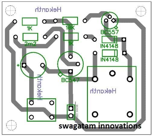
PCB Design
Long Duration Timer using Op Amps
The disadvantage of all analogue timers (monostable circuits) is that, in an effort to achieve fairly long time periods, the RC time constant needs to be correspondingly substantial.
This inevitably implies resistor values of greater than 1 M, that may result in timing mistakes caused by stray leakage resistance within the circuit, or substantial electrolytic capacitors, that similarly can create timing problems because of their leakage resistance.
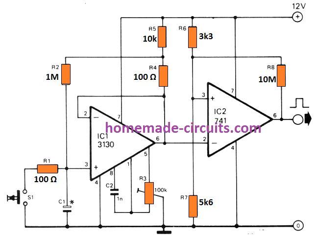
The op amp timer circuit shown above accomplishes timing periods as much as 100 times more time compared to those accessible using regular circuits.
It achieves this by lowering the capacitor charging current through a factor of 100, consequently improving the charging time drastically, without requiring high value charging capacitors. The circuit works in the following way:
When the start/reset button is clicked C1 gets discharged and this causes output of op amp IC1, which is configured as a voltage follower, to become zero volts. The inverting input of comparator IC2 is at a reduced voltage level than the non -inverting input, hence the output of IC2 moves high.
The voltage around R4 is around 120 mV, which means that C1 charges via R2 with a current of approximately 120 nA, which apprers to be 100 times less than what could be attained in case R2 had been attached direct to positive supply.
Needless to say, if C1 had been charged through a consistent 120 mV it could rapidly achieve this voltage, and stop charging any further.
However, the lower terminal of R4 being fed back to the output of IC1 ensures that as the voltage across C1 goes up so does the output voltage and therefore the charging voltage given to R2.
Once the output voltage climbs to approximately 7.5 volts it surpasses the voltage refernced at the non-inverting input of IC2 by R6 and R7, and the output of IC2 becomes low.
A tiny quantity of positive feedback supplied by R8 inhibits any kind of noise existing on the output of IC1 from getting boosted by IC2 as it moves from the trigger point, because this normally produce false output pulses. The timing length can be calculated by the equation:
T = R2 C1( 1 + R5/R4 + R5/R2) x C2 x ( 1 + R7/R6)
This may appear somewhat complex, but with the part numbers indicated the time interval can be set as long as 100 C1. Here C1 is in microfarads, let's say if C1 is selected as 1 µ then the output time interval will be 100 seconds.
It is very clear from the equation that it is possible to vary the timing interval linearly by substituting R2 with a 1 M potentiometer, or logarithmically by using a 10 k pot in place of R6 and R7.
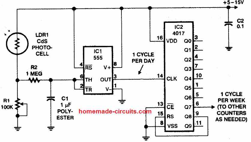
Long Duration Timer using LDR for Day Night Sensing


With over 50,000 comments answered so far, this is the only electronics website dedicated to solving all your circuit-related problems. If you’re stuck on a circuit, please leave your question in the comment box, and I will try to solve it ASAP!
Sorry for the mistake! Most of the values are already in the diagram. But only the capacitor value is required! Please advise Sirji !!
Thank you!!
Maddy, which diagram are you referring to? The design using a single IC 4060 or the 4060 + 4017 combo?
If possible, can you please provide me the component values to arrange. Thank you again, Sirji!!
I would be using the Automatic power switch ON reset ckt in that article!
Good noon Sirji,
I want to upgrade my 555 Timer to this one!
https://www.homemade-circuits.com/how-to-understand-ic-4060-pin-outs/
My question is- For a precise 50m switching time, is it okay to use single CD4060 Timer? Or should I go for CD4060+CD4017 combo, as given here in above article? I would be having a 15m window for the switching purpose, after the 50m Me elapses!
Please advise!! Thank you!!
Hi Maddy,
The IC 4060 alone can handle a precise 50 minute switching timing, provided the capacitor quality is high quality, and is a non-polar type, like a PPC or metalized polyester. And the DC power supply must be clean and fully regulated.
That said, the CD4060+CD4017 combo can provide even greater precision, no doubt about it.
And what if we can arrange another timer to give that one shot momentary push via a relay? I do think we can have it!!
Am I assuming in the right way Sirji?
Thank you!!
I am not sure how looping of two similar circuits will work, because they both must work alternately.
IC 4060 option is the recommended circuit for your application, which will give you perfect results.
It will alternately toggle the two loads after 50 minutes each, as per the adjustments.
Morning Sirji!!
Can we have above BJT timer without any push button? That will ease the way this ckt needs to be operated ie without our requirement to push the button for every new cycle of charging the capacitor! Can we arrange such facility?
Thank you !!
Good Morning Maddy,
No, the BJT circuit cannot be used without a push button because it is a one-shot timer circuit.
One problem Sirji!!
How come
T_ON = 0.001923 seconds ≈ 3000 seconds (Correct)
And same for T_OFF?
It should have been very easy for me to grab the component values and move on, but anyone who comes to your site and goes through these lines will find this particular line extremely confusing! Both are in seconds! Is something missing? Please give some more time to clear!!
Thank you again!!
You want the two loads to alternately toggle after 50 minutes each, right, so 50 minutes = 3000 seconds.
My present 555 timer ckt has 2200uF(50v)+470uF(16v) combo in parallel just to have 18-20m switching time. And I’m sure if the Capacitor values rises then the Resistor values should decrease proportionately. Am I right Sirji?
And Thank you for the Specialised solution and for expending your precious time to solve my problem, Guruji !!
Yes, if the capacitor value increases the resistor values will decrease proportionately, and vice versa.
That’s it! You got it accurately,Sirji !! Both the points mentioned by you were my mistakes. Yes, I changed the input voltage and included a capacitor rated at 16V. But I can manage them as they are still working. But my problem still remains that I need to adapt a 50m switching time in the timer having a 12v relay at the end. I would be operating two identical DF players with these relays. Each one plays an MP3 that is atleast 50m long. So I need to have such arrangement for the DF player so that the Timer switching occurs after the MP3 ends, not in the middle. So what should be changed in the BJT ckt or the existing 555 timer for this purpose?
Thanks again!!
Thank you Maddy,
I have updated the detailed calculations with the part values in the following article, although the resistor values looks impracticable.
https://www.homemade-circuits.com/alternate-switching-relay-timer-circuit/
If you don’t get proper results then you may have to go for a 4060 IC based circuit:
Morning Sirji, I want to build above BJT timer ckt to get an accurate switching time of 50m between two loads, but without any push button. I already have made another switching 555 ckt from your site –
https://www.homemade-circuits.com/alternate-switching-relay-timer-circuit/
It worked flawlessly for initial few months but now it’s switching time is getting shorter and shorter. Now I’ve got this BJT ckt and I think it’s more better than 555 timer for the reasons you have mentioned here in this article. But now I have two options left. First, to build this BJT timer ckt without any push button. And second, to adopt such diode-resistor trick (used in this BJT ckt) in my 555 timer. Please advise!
And A Very Happy New Year Sirji!!
Thanks Maddy, for updating the info, Glad the circuit is working for you. And Happy New Year to you in Advance…
The 555 circuit is already too good and will never deviate from its timing unless the input voltage varies.
Please include a 7812 IC to power the circuit so that the IC timing remains constant.
And also please make sure the timing capacitor is of very good quality rated at minimum 25V.
Hi, can I use ic 555 instead of 4060 in the first circuit, because here 555 is the only one I can access
Hi, you can use it but it won’t provide accurate time intervals like 4066 IC
hello, from you get the pin 16 in the first circuit can you explain as soon as possible please .
Pin16 is the supply positive or the Vcc pin for both the ics, 4017 and 4066…
what is the replacement of ic44060 i cant find it near me
I think it is ic 4020, but the pinout configuration may be different, please check the datasheet of the ic…
Great site! I discovered you site while teaching my grandson electronics.
The long time delay using the 4060 and 4017 is almost identical to the timer I’ve been building with him on breadboard.
My question is please where can we purchase the PCB board you have kindly designed? Here in uk PCB company’s are extremely expensive.
Please let me know if you have the facility to produce these for sale.
Many Thanks Steve
Thank you, glad you liked the site, however unfortunately I no longer manufacture PCBs, so it may not be possible for me to make it for you. Procuring a single piece can be always expensive no matter which country you are in. I would rather suggest you to build the circuit on a stripboard by soldering the parts which will produce more accurate results. Please let me know if you have any further questions.
I refer 1st circuit in this delay calculation formula Delay Period = 2.2 Rt.Ct.2(N -1) has been given. can you clear me N stands for what
N stands for the Q number, Q1, Q2, Q3 Qn….please see the figure 1 in this datasheet:
https://www.st.com/resource/en/datasheet/m74hc4060.pdf
In your BJT timer circuit what is the maximum time I can get in this circuit and what components should I use to get an adjustable timing upto 8 hours
Hi Val, In the BJT timer circuit 8 hours may not be feasible. You will have to employ the first circuit for an 8 hour long time delay.
Hello Swagatam,
I like your article!
I am interested in using design no. 2) “Using Only BJTs”.
What is R in the formula?
If I am feeding my capacitor straight from the supply voltage, like in your drawing, surely Vs = Vc, right?
In that case Vc/Vs = 1, and then ln(1) = 0, which does not yield a result.
How can I calculate the delay time of this circuit?
Thank you dng,
R indicates the 2M2 resistor.
I got this formula from Wikipedia.
I think it is better to check the timing practically by using arbitrarily selected RC values, and then finding out the intended values through simple cross multiplication, since the operation is very linear and proportional.
Thx Swagatam,
I tried to calculate the time for the OpAmp circuit you show towards the end of the article, but I cannot get the 100s for the case where I use your standard values shown and a 1 uF value for C1. I converted all the R values into Ohm, and the C values into uF.
Could you pls tell me what I am doing wrong?
R1 100 Ohm = 100 Ohm
R2 1 MOhm = 1000000 Ohm
R3 100 kOhm = 100000 Ohm
R4 100 Ohm = 100 Ohm
R5 10 kOhm = 10000 Ohm
R6 3.3 kOhm = 3300 Ohm
R7 5.6 kOhm = 5600 Ohm
R8 10 MOhm = 10000000 Ohm
C1 1 uF = 1 uF
C2 1 nF = 0.001 uF
T = R2 C1( 1 + R5/R4 + R5/R2) x C2 x ( 1 + R7/R6)
T = 1000000*1*(1 + 10000/100 + 10000/1000000) x 0.001 x (1 + 5600/3300)
T = 272420.909 s
Hi dng,
The R2 and C1 are the main timing components, which you can adjust until you get the desired time delay at the output. I still believe doing the practical trial and error method which can enable you get the perfect and the most precise component values for the required delays.
You can probably try the following modification in your calculation:
100 = R2*C1*(1 + 10000/100 + 10000/1000000) x 0.001 x (1 + 5600/3300)
I liked the plain transistor circuit because of it’s simplicity. I tried the circuit with a 4000uF cap, but only achieved marginally longer delays (a few seconds). Increasing 2k2 causes the circuit to become unresponsive.
The base resistor of BC547 is 2M2 not 2k2, and it can give very long delays, I have tested it myself and I could achieve very long delays, you might be doing something wrong in the circuit.
Very educational and helpful. I need a circuit that turns ON for 5 hours and OFF for 19 hours. Needs to be low power and uses 5VDC or less.
Thank you Jose,
You can try the following concept with appropriate adjustments:
https://www.homemade-circuits.com/how-to-make-simple-programmable-timer/
I need a circuit that has a 30 day timer, and can power a small motor at the end of the 30 day timer, until the motor or attached mechanism trips a momentary switch, and then the 30 day timer restarts.
I think the following concept can be tried for your application:
https://www.homemade-circuits.com/making-programmable-timer-circuit-using/
i need two chambers working alternative with 6 hrs delay and if one is damaged the remaining should on circuits
i need hard ware design or any module which is suitable send me i will purchase
You can try the following circuit:
https://www.homemade-circuits.com/how-to-make-simple-programmable-timer/
Sorry, ready-made prototype cannot be supplied from this site.
Hello sir, Good morning.
sir, this is with regard to the first design in this article. I want to run three different loads to on and off at two different delay periods. Is it possible sir.
with thanks,
leelesh
Hello B.K.
you can definitely use the first long duration timer concept to accomplish your application, for running 3 different loads, each with two different sets of ON/OFF delay periods.
Thank you sir,
Hello engineer, I need help to design a timer with a unique 4060 if it is possible. I need an on time of 30sec and an off time of 1min. I can do it with a 555 and a 4017. But since the 4060 has its own oscillator I would like to try it and with this I save space and money. I appreciate if you can make an outline and your kind attention. Thanks.
Hello Jesus, I will try to design it for you and let you through this comment soon….stay tuned.
Hi Swagatam, you have created a great site, I discovered it during my search for a very long duration delay on timer, that I need to source or get someone to make; what I need is a low cost, reasonably accurate delay timer, that can be started manually by bridging 2 pins, it will time down for 3 or 6 months, (that is previously set to either of times as required) at the end of the period it turn on a relay to turn on an external flashing LED indicator light. The timer would be restarted manually as required by either bridging the 2 ‘start’ pins or another set of pins
Do you know of any such timer or anyone interested in making say 40 units as soon as possible, any assistance would be greatly appreciated Thanks John Callaghan
Thank you John, to get the required results you can upgrade the first circuit from the above article, by adding more number of 4017 ICs with the existing 4017 IC. The transistor relay driver can be removed from the shown position and the same can be attached to the selected output of the last 4017 IC. To reset the entire circuit, you can connect all the pin15 of the 4017 ICs, and connect a push button parallel to C2.
Hi Swagatam thanks for you very informative reply, it seems like it is the solution to my problem; I now need to get someone to built me a prototype with a 6 month timing period, so i can assess its operation, do you know of anybody that may be interested, I am happy to pay a reasonable price for a working prototype.
Thanks a Lot for your assistance
All the Best
John
Thank you John,
At the moment I do not know anybody who can assemble a practical prototype for you, however I will inquire about it, if I find somebody suitable, will inform you regarding the same.
Hello Swagatam,
I made the first circuit using 4060 IC and 4017 IC. Please tell me how to calculate the P1 value to get impulses with 60 min intervals from 4060 IC. So the time interval between 4017 IC pin would be 1 hour. please show me the calculation. Thank you very much.
Hello Upul, The formula is given in the article, but I have never used it so can’t confirm its results….the easier way is to check it by some trial ans error. For example if the P1+R2 value is 500k, and C1 value is 0.1uF which gives a timing of 30 minutes, then if C1 value is made two time more to 0.2uF will produce 1 hour timing output from the 4060. Therefore, the response is very linear. You can test with a small capacitor to get the sample timing, and then dimension the capacitor accordingly to get the desired time output from the 4060 IC
Thank you so much for your quick reply. The answer is very useful for me. I can try this and get my work done. Thank you so much for publishing this kind of circuit diagram. wish you all the best.
You are most welcome Upul!
Thanks for sharing.
I want to ask about the third circuit that using OP-AMP IC. What is the resistance value of R3 (trimpot) to be set when building this circuit?
It is 100k preset
Swagatam,
I made a simple monostable mode 555 circuit and it works perfectly with an LED at the output. However, when I try to connect the output to a relay switch, it switched at first but then it wont return to original state. I tried the whole process on Multisim, and it only works once – switch on and off, after that nothing switch at all no matter how many time I hit the virtual button . I’m not sure where im tripping at. Could you help me?
I look around where to upload my schematic for an easier look or even your email so I could contact you but couldn’t find any.
Hi Vu, did you build it practically by using real parts? Soft wares can be misleading, but if you build it physically it will surely work. You can refer to the examples presented in the following article
10 Best Timer Circuits using IC 555
Relay can be connected directly across pin3 and ground with a protection diode across the relay coil
Hi Swagatam,
What is N in this formula?
Delay Period = 2.2 Rt.Ct.2(N -1)
Hi Vu, N corresponds to the pinout sequence number among the outputs of the IC 4060
Hi Swagatam,
Can you help me with how to make a timer circuit that first count the switch off time then close, count the switch on time then off. More like off (timer) –> on (timer) –> off.
Both timers are desired to be adjustable around 1 minute to 1 hour.
Thank you in advance!
Hi Vu, You can try the following design, it is exactly what you are looking for!
Simple Programmable Timer Circuit
Swagatam,
Thank you for your response. I have checked out the link provided, currently trying to gather the parts but when I watched the video, I realized that this schematic repeats itself with infinitely loop, and that’s not what I wanted. I only need it to run 1 loop, no repeating. Could you help me with that?
Hi Vu, the diode across pin#3 and pin#11 of the upper IC latches the system and enables the circuit to work in a one-shot monostable mode, removing this diode allows the circuit to work in a cyclic manner.
I am interested in this IC 4060 and IC 4017 timing circuit. How can I
add a circuit to this circuit, to set a time range when I go out of Home.
Please help me.
You can try the second concept, and use the S1 switch for programming the timing, along with the 500k pot P1
Hello, I’m interested in apply the first circuit. I need to make the NO and NC change in 5.5 hours (5 hours, 30 minutes). I’m not sure how to use equations to calculate resistances and capacitors, specially because in Delay piriod has a N parameter that I don’t know what it is.
Thank you for your answer
Hello, if the ON and OFF timing are equal then you can implement it using a single IC 4060 stage, the IC 4017 can be ignored and removed.
For timing component value calculation, you can first determine any small random timing using random R and C values. Once the random time value is found using random parts, you can use them as the sample yardstick to determine the 5.5 hour values.
More can be learned in the following article
https://www.homemade-circuits.com/how-to-make-simple-programmable-timer/
Hi,could this circuit be adapted to run on a single 18650 battery ? voltage range 4.09 to 2.90 -i have been given & built 2 circuits for an xmas log reindeer which both run on the 18650 and start thro a LDR at dusk(it gives the circuit/s a virtual ground) but continue all night whereas I like to switch them off after say 8 hours and start again the next night, i believe the hef4060 is lower voltage
Hi, yes except the last one, all can work with 3 V and above supplies. All CMOS and BJT based circuits can work using supplies as low as 3 V….but the indicated relay cannot be used, unless it is also rated at 3 V.
thank you for the swift reply,so as i don’t need a accurate timer just a long timer ,would a 555 coupled with a cd4017 produce a good enough result rather than order a 4060 ?
Yes, 555 IC and 4060 combination can be used for reasonably long duration delays
Hi,
Can I use long duration timer circuits with 5V-6V power source?
I would like to use it with ESP32 because it keeps ESP32 code simple.
Hi, yes 6V will also work for the proposed long duration timer designs.
Thank you Swagatam
Hello Swagatam,
do you have any idea about circuit that can give me delay of 240Hours
1. I should have provision to set/ reset the time anywhere between 0-240 hours i can use one push button for setting the time.
2. switch to selet the mode set or reset
Hi Lokesh, you can easily extend the timing output to any desired levels, along with the facility to adjust the ranges, by including additional IC 4017 stages as required. One example is given here:
https://www.homemade-circuits.com/making-programmable-timer-circuit-using/
Selector switches can be added between each 4017 IC for enabling a wide range of timing selection.
Hello Swagatam
Regarding the 24 hours timer circuit using IC 4060 and IC 4017
(the first circuit in this article)
After it counted 24 hours and start activating the relay …
How long the relay will be open in seconds or minutes or is it just a one time quick trigger?
And how to control that time to make it adjustable from 10…20..30 seconds to 1 or 2 or 3 minutes for Relay to remain open?
if i want to connect a DC 12 Volts Motor to the relay
can i put pot variable resistor or change capacitor somewhere ?
and can i use ic 555 timer for 30 seconds or 1 minute after the relay and how?
Sorry for many questions
Writing your helpful detailed answer will be Greatly appreciated
Thank you very much
Hello felix, to make the circuit repeatable you must remove the 1N4148 diode D1. The IC 4017 has 10 outputs in the order: 3,2,4,7,10,1,5,6,9,11
The timing will start from pin3, and end at pin11, then go back to pin3 and so on.
The timer interval between each pin will depend on the time interval generated by the IC 4060 output pin3. if it is set for 1 hour, then each sequence across the 4017 output will be separated by 1 hour, producing a total delay of 10 hours.
The connection of the R4 will determine the ON and OFF timing of the relay. If this is connected at pin10 then the ON/OFf timing will be 50%, and so on.
You can connect amotor to the relay. You can connect a IC 555 monostable for delay ON after the relay
Hi Swagatam,
I am looking for a circuit to switch on another circuit(alarm) for 1 minute every hour on the hour. I would like the circuit to be accurate, (like a clock) so I was thinking of a DS3231 RTC for the time keeping. Can this be done without a lot of extra components and without an Arduino or other micro controller. I have it designed with a CD4060 timer with resistors and capacitors and a preset to try to adjust to the 1 hour time. Surely you have run across a similar requirement and will have a simple circuit to accomplish this. Thanks for your time! I really appreciate you and your good work.
Hi Norman, You can probably try applying the following concept and then divide the result using a IC 4017 circuit, and subsequently feed it to pin11 of IC 4060 for getting the required 1 hour intervals
https://www.homemade-circuits.com/1-hz-to-1-mhz-frequency-reference-generator-circuit/
Hello sir, please I need 1hr on and 1hr off timer circuit that will works continuously, which one will do.thanks
Hi Adeyemi, you can simply configure a 4060 IC as per the instructions provided in the following article, and acquire the output from pin3 of the IC.
https://www.homemade-circuits.com/how-to-understand-ic-4060-pin-outs/
Please the second design(btj) on this page will likely give how many hours delay
I don’t remember it, you will have to test it practically once to know the range.
Hi Swagatam,
When power is switched off how will capacitors c1 and c2 discharge so that when power is again switched on circuit works from begining
Hi Hemant, C2 will reset the IC and force C1 to discharge.
Hi sir .
Thank you for your useful information
In case last circuit of delay accurate time duration…. how much delay time will get to off relay .as same component use…. ?
Thanks as advance.
Hi Ghyas,
the time will depend on the 2M2 resistor and the 1000uF capacitor You will have to find it through practical trials.
Sir,
I want to make a delay circuit of 6hr, can you provide values of resistors and capacitors…or can you elaborate more about selection of resistor Nd capacitor according to time delay needed.
Hemant, use any random resistor for P+R2 say for example 100K, and 1uF for C1 non plar.
check after how much time pin3 goes high…let’s say this time is A seconds
now use the following formula to get the 6 hour resistor
100/R = A/21600
R will be the required resistor in kohms for 6 hours or 21600 seconds
Sir,
I have built this circuit in baro- board but i am facing issue of reset. My circuit is not resetting when power is switched off.
I have used polar capacitors instead of non polar. What can be the reasons?
Hemant, did you connect C2 with the circuit? C2 will reset the circuit whenever the power supply is turned OFF and ON again.
Polar cap for C2 will do!
Connect a 10K across the +/- line of the circuit also to discharge the filter capacitor of the supply when switched OFF.
Hello @ Swagatam, hope you are well.
Kudos for the good work…
I’m trying to build an incubator, I would like to know how set up the timer configuration so that a motor turns the eggs in opposite directions every 3hrs or 6hrs. That is the timer output gives a high for 3 or 6hrs and then switches to low for another 3 or 6hrs. I need it to be continuous (cyclic)… Thanks
Thanks Rob, you can try the 3rd and the 4rth concepts from this page. If you have any doubt please let me know!
https://www.homemade-circuits.com/?s=incubator
Thanks for your prompt response…. I found the various circuits interesting, though some were confusing to me.
The one I can understand easily is this https://www.homemade-circuits.com/submersible-pumpset-timer-circuit/.
So I wanted to ask you if it is possible to set this (submersible-pumpset-timer-circuit) to 3 hours or above as well. I have thought of a way to incorporate it with a dpdt and limiting switches(for the motor).
Hoping to hear from you soonest. Take care.
Sure, you can use it for 3 hours delay, but it won’t give you a separately adjustable 2-stage time delays. The time intervals will be ON and OFF with equal duration. For getting two independent adjustable delays you can perhaps try this concept:
https://www.homemade-circuits.com/how-to-make-simple-programmable-timer/
OK, thanks very much for all the time and help. I will try to build both and make use of the one that is more efficient.
I really love your website, and find it very educating and useful, you are a blessing to the engineering community. Keep up the good work and remain blessed.
You are most welcome, wish you all the best!
How many Ic4017 will be needed to give 3months. Thanks so much Swagatam.
that will depend on what delay you select for the IC 4060 pin#3.
I am getting it but not fully, what about other pins of second ic4017
No change with the other pins, they will connect exactly same as the first 4017, except the feedback diode which will always connect across pin#11 of 4060 and the pin#11 of the last 4017 in the line.
Sir,I want to make 2hrs on time and 2hrs off time repeatedly working timer circuit can you help me giving daigram
Hi Vipul, you can select any 4060 IC based timer circuit and get the required output, a example circuit is shown below
https://www.homemade-circuits.com/submersible-pumpset-timer-circuit/
Is the C1 & C2 are electrolytic capacitor. If so what about polarity?
No, those are non-polar
Thanks for your quick reply
Hi. Swag
a question.
is it posible to make this timer a repeat timer ?????.
i have some repeat timers from Rons website but they are not working as they should work.
after 2 runs they stop working even with the resistor between the pins 8 and 16.
i have desided that i wil make my light instalation for my aquarium with timers and fading leds so the effect wil be almost the same as we spoke earlier.
i hope that you can help me out here.
the lost of voltage with the dimmer is solved.
as you say simply the collectors direct at the positive and the leds on the emiters.
other posibility is to use a second power supply and put the collectors on that one with a little higher voltage.
it was verry helpfull what you told me and i dig a little more in to it and try to understand the matery better than i did at that time.
hope to hear from you soon .
Johan. the dutchman
Hi Johan,
In the above circuit you can make it work as a recycling timer, simply by removing the entire D1 link, and the ON/OFF ratio can be also modified by changing the T1/R4 connection configuration with the IC output pinouts.
for your question regarding the LED location in emitter side and raising the collector voltage, I am sorry that will not help because the emitter voltage will be always less by 0.6V than the base voltage value, no matter what voltage you try on the collector side…therefore the emitter LEDs will follow the base voltage regardless of the collector voltage.
thanks sir,,,
my pleasure!
Hi, Admin,
I need 3 kinds of circuit which is for the paddy field pest control light(LED) up to 40LED which can be run on 9V battery or 6v AA battery.
Conditions are below.
1) Switch on the unit(40led light run with 9V or 6v battery) and it should off 2hrs 30min to 3hrs.
2) Auto switch on when out door light dims then Auto off after 2hrs 30min to 3hrs.
3) sl no 2 with solar charger..
Purushottaman,
you can try the last circuit presented in the following article
https://www.homemade-circuits.com/2014/09/solar-garden-light-with-programmable.html
You will need to use 12V AAA battery, by connecting 8 AAA 1.5V cells in series, connect 2 such series in parallel…16 AAA cells in all
Thanks for your response at admin…
you are welcome!
Thanks admin! Pls am using Proteus on my PC before but I mistakenly uninstall it and I was unable to install it back……
sorry I do not have any solution to that problem!!
Good evening. Pls I need a circuit that can switch between 3loads with 4 hours intervals
you can use the same circuit as shown in the above article, with the following modifications:
use 2, 4, 7 as the outputs for the loads, and connect pin#10 with D1 anode….ignore pin#11 keep it unconnected.
set pin#3 of IC 4060 for 3 hour clocks
Dear Swagatham,
can you please modify this circit as follows
I have a 12hr mode Quarts clock with needles. My idea is to fix 12 LED's at each hour positions. One LED should lit at a time. Eg, if time is 3'O Clock, third LED should glow. After 1hr 4th LED should lit. This process continues.
By this arrangement, it is easy to understand the time at night by the LED position.
I know, CD4017 have only 10 otputs, I think, two CD4017 can be cascaded to obtain 12 outputs. If yes, design that way, otherwise, use any different IC have 12 outputs.
Dear Anil, you can do it the following way:
connect the pin13 of the first IC 4017 with its own pin11, which is last or the 10th output.
connect this junction with the base of a BC547 through a 1K resistor, connect the collector with pin#8 of the second 4017 IC. connect emitter with ground.
finally connect the pin#7 of the second 4017 with pin#15 of the first through a 1K resistor, remember you must disconnect the pin#15 of the first IC 4017 from ground before doing this.
also make sure to connect a 0.47uF capacitor positive to Pin#15 of the first IC.
Pi#15 of the second IC can be connected with ground, but remember to connect pin#14 of both the ICs together.