
In this article I have explained the pinout functions of the IC SG3525 which is a regulating pulse width modulator IC. So I have explained in details:
Main Technical Features
The main features of the IC SG3525 may be understood with the following points:
- Operating voltage = 8 to 35V
- Error amp reference voltage internally regulated to 5.1V
- Oscillator frequency is variable through an external resistor within the range of 100Hz to 500 kHz.
- Facilitates a separate oscillator sync pinout.
- Dead time control is also variable as per intended specs.
- Has an internal soft start feature
- Shut down facility features a pulse by pulse shutdown enhancement.
- Input under voltage shut down feature also is included.
- PWM pulses are controlled through latching for inhibiting multiple pulse outputs or generation.
- Output supports a dual totem pole driver configuration.
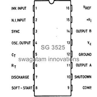
Pinout Diagram of the IC

SG3525 PinOut Description
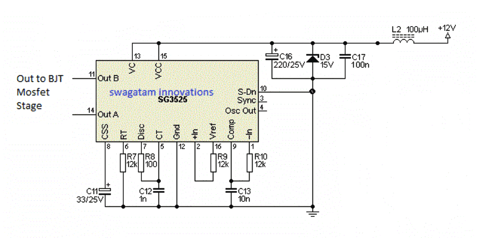
A practical implementation of the following pinout data may be understood through this inverter circuit
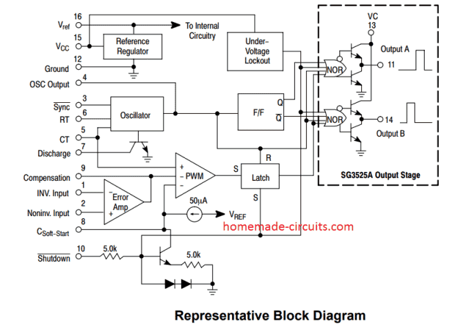
The IC SG3525 is a single package multi function PWM generator IC, the main operations of the respective pin outs are explained with the following points:
Pin#1 and #2 (EA inputs): These are inputs of the built-in error amplifier of the IC. Pin#1 is the inverting input while pin#2 is the complementary non-inverting input.
It's a simple op amp arrangement inside the IC which controls the PWM of the IC outputs at Pin#11 and Pin#14. Thus these EA pins 1 and 2 can be effectively configured for implementing an automatic the output voltage correction of a converter.
It is usually done by applying a feedback voltage from the output through a voltage divider network to the non-inverting input of the op amp (pin#1).
The feedback voltage should be adjusted to be just below the internal reference voltage value (5.1 V) when the output is normal.
Now, if the output voltage tends to increase above this set limit, the feedback voltage would also increase proportionately and at some point exceed the reference limit. This will prompt the IC to take necessary corrective measures by adjusting the output PWM, so that the voltage is restricted to the normal level.
Pin#3 (Sync): This pinout can be used for synchronizing the IC with an external oscillator frequency. This is generally done when more than a single IC is used and requires to be controlled with a common oscillator frequency.
Pin#4 (Osc. Out): It's the oscillator output of the IC, the frequency of the IC may be confirmed at this pin out.
Pin#5 and #6 (Ct, Rt): These are termed CT, RT respectively. Basically these pinouts are connected with an external resistor and a capacitor for setting up the frequency of the inbuilt oscillator stage or circuit. Ct must be attached with a calculated capacitor while the Rt pin with a resistor for optimizing the frequency of the IC.
The formula for calculating the frequency of IC SG3525 with respect to RT and CT is given below:
f = 1 / Ct(0.7RT + 3RD)
- Where, f = Frequency (in Hertz)
- CT = Timing Capacitor at pin#5 (in Farads)
- RT = Timing Resistor at pin#6 (in Ohms)
- RD = Deadtime resistor connected between pin#5 and pin#7 (in Ohms)
Pin#7 (discharge): This pinout can be used for determining the deadtime of the IC, meaning the time gap between the switching of the two outputs of the IC (A and B). A resistor connected across this pin#7 and pin#5 fixes the dead time of the IC.
Pin#8 (Soft Start): This pinout as the name suggests is used for initiating the operations of the IC softly instead of a sudden or an abrupt start. The capacitor connected across this pin and ground decides the level of soft initialization of the output of the IC.
Pin#9 (Compensation): This pinout is for compensating the error amplifier op amp. Mostly this pinout is connected to ground via a RC network. However, if required this pinout can be configured with an external transistor which can ground this pin during a critical situation, enabling a shutdown of the IC output.
Pin#10 (Shutdown): As the name suggest this pinout may be used for shutting down the outputs of the IC in an event of a circuit malfunction or some drastic conditions.
A logic high at this pin out will instantly narrow down te PWM pulses to the maximum possible level making the output device's current go down to minimal levels.
However if the logic high persists for longer period of time, the IC prompts the slow start capacitor to discharge, initiating a slow turn ON and release. This pinout should not be kept unconnected for avoiding stray signal pick ups.
Pin#11 and #14 (output A and output B): These are the two outputs of the IC which operate in a totem pole configuration or simply in a flip flop or push pull manner.
External devices which are intended for controlling the converter transformers are integrated with these pinouts for implementing the final operations.
Pin#12 (ground): It's the ground pin of the IV or the Vss.
Pin#13 (Vcc): The output to A and B are switched via the supply applied to pin#13. This is normally done via a resistor connected to the main DC supply. Thus this resistor decides the magnitude of trigger current to the output devices.
Pin#15 (Vi): It's the Vcc of the IC, that is the supply input pin.
Pin#16: The internal 5.1V reference is terminated through this pinout and can be used for external reference purposes. Example, you can use this 5.1V for setting up a fixed reference for a low battery cut-off op amp circuit, etc. If it's not used then this pin must be grounded with a low value capacitor.
With over 50,000 comments answered so far, this is the only electronics website dedicated to solving all your circuit-related problems. If you’re stuck on a circuit, please leave your question in the comment box, and I will try to solve it ASAP!
UC3525 Half bridge converter output voltage increases 2V, to 3V from set voltage
sir please can you help me out with the formula solving
sir i want laminating transformer full data.
You can refer to the following article:
https://www.homemade-circuits.com/how-to-make-transformers/
swagatam sir i want 7amp18vdc to 14vdc regulating power supply for lead acid battery charging
You can try any LM338 based power supply. Use two LM338 in parallel.
ckt diagram pls sir
Please refer to the LM317 based circuit, replace the LM317 with LM196 or use two LM338 in parallel:
https://www.homemade-circuits.com/how-to-make-current-controlled-12-volt/
hai sir i have one drought ,sir can run 24v operating voltage inverter transformer, to 12v.
sreenivasulu, I cannot understand your question.
24v operating inverter , can run 12v operating supply, in case 24v inverter secondary side winding modification , i mean 12 0 12v,
24V inverter cannot run on a 12V battery, for modification, rewind the DC side winding to 9-0-9V
it will runs 12v sir
if you run a 24V transformer with 12V then the output will be 50% lower.
swagtam sir if 1000w inverter trasnsformer priymariside turns reduced i mean 230v turns data ,reduced 60v will increase amps. can i give e bike operating voltage 60v, 18amp.
Yes it will increase the amps proportionately.
swagatam sir how can convert 200w , to 500w inverter ckt board.
You can do it by upgrading the mosfets, battery and the transformer.
sir pls say high amp mosfet number and transformer rating that means amps rating, can i use same ckt board
sreenivasulu, please tell me the power (watts) of the inverter that you want to build and which circuit diagram?
i am purchased amazon 200w kit irf 44n, pulsmodular ic sg3524 using ,for amlification boosting bc547 npn used thats kit.
First try the board and check whether you get 200 watt power output or not….if the boards works correctly, then you can upgrade the MOSFETs by replacing them with IRF3205 (3 in parallel). The battery must be also upgraded to 200 Ah….
18 amp transformer will produce only 10 x 18 = 180 watts….so it will not work for a 1000 watt output
which amp rating transformer suitable sir
For 1000 watt inverter, divide 1000 by the battery voltage that will give you amp rating of the transformer.
can runs atx transformer, 3 atx transformers , 3 nos 200w boards,and individual for 100ah 12v battery.
If you want to use ferrite transformers then its winding will need to be calculated.
winding cliculation formula need sir, can generate 70v,12 amp with help of ferrite core transformer. then connect 3sets connect o/p voltages in parllel 70v,36amp.can get using e bike operating voltage .
You can refer the following article, but i cannot help with the calculations, you will have to do it yourself:
https://www.homemade-circuits.com/how-to-design-and-calculate-ferrite-core-transformers-for-inverters/
sir can i use 200amp inverter welding machine ferrite core transformer.
Without calculating the winding and matching the circuit frequency you cannot use any ferrite transformer.
i have 10v 0v 10v transformer 18amp . it can useful sir,further upgrading 5oow .convertion.
swagatam sir sg3524 and sg3525 both are same or not,
Yes, both are same with their basic functions, but please refer to their datasheets to confirm the pinouts
What is Maximum output current of sg3525.can I drive directly irfp250 MOSFET.
You can drive the MOSFETs directly from the SG3525 outputs, MOSFET gates do not require high current to operate.
Hi swagatam
Please sir which this, is the real formula “1/CT(0.7RT+3RD)” or “(1/CT(0.7RT+3RD))(0.5)” in calculating the frequency in this IC SG3525
Hi Emmanuel,
The formula is
f = 1 / Ct(0.7Rt + 3RD)
The PWM frequency relies on the timing capacitance and resistance, with the timing capacitor (CT) linked to ground through pin 5 and the timing resistor (RT) connected to ground through pin 6. Additionally, the deadtime is determined by the resistance between pins 5 and 7 (RD) and to a lesser extent, this value also affects the frequency.
i know all those connections but I’m confused with the formula because I find out that the IC can only oscillate from 100Hz to 100KHz and if needed for 50Hz on the output of a transformer one need to calculate for 100Hz and multiply it with 0.5 which is 50%. So I need clarification on this please.
Yes, what you have learned is correct, but since the IC can oscillate at a minimum 100 Hz, it cannot go down to 50 Hz. You will have to use a divide by two stage for getting 50 Hz.
Thanks for your quick response.
I would have like to see your prototype for the SPWM chopping aspects of your SG3525 inverter so to see the output waves form of the design.
No problem, If I happen to build a prototype I will surely let you know and show you the waveform.
Thanks you very much and keep up the good work.
You are welcome Emmanuel!
Swagatam,
I am trying to get a smooth control of PWM using the SG3525 especially when using an optocoupler which only has a small adjustment range on its input. Most of the circuits I have tried give me either no output i.e. PWM too narrow or normal output i.e. no PWM control with nothing in between.
What am I doing wrong? Is there a circuit which I could use which allows me experiment with the range of control?
Hello Paul, please explain the schematic that you have used, without understanding the schematic it can be difficult me to suggest.
please someone help me to know more about compensation in sg3525
Hello again, for a push pull transformer would I have to reduce the oscillator frequency in half for transformer calculations?
The oscillator frequencies at pin#11 or pin#14 should be 50 Hz, if 50 Hz is required at the transformer output, or 60 Hz if 60 Hz is required at the transformer output.
Thank you! On the datasheet I do not see suggested values for soft start capacitors or a max/min value. Would 1 pf work?
In some schematics I have seen pin#8 connected directly to ground when not used. I would prefer connecting a small value capacitor instead…yes a pF will work.
Hello, to disable soft start can I leave pin 8 floating?
Thanks,
Jon
Hi, I am not very sure about it, it is better to keep a very small value capacitor connected, such as a 0.001uF or similar.
Hi,
Please i will like to know the pin of sg3525 that is called PWM feed or the pin that two diode in sine wave can be fed to when using sg3525 as PWM oscillator in design a pure sine wave for inverter.
Regards,
Sina.
Hi, according to me there’s no such pinout which can be used to convert the IC SG3525 into a pure sine wave inverter.
I am ANURA SENANAYAKE. From sriLanka. I am a goverment nursing officer. But Iam an electronics hobbiiest. I always follow you. I preferred your articles. Wish you a bright future.
Thank you so much Anura! I appreciate your kind feedback!
Hi swag..
I build an smps inverter using the sg3525
When I power on the upper fet is very hot and the lower fet is cool and without load at the output of transformer. so I swaped the drain pin of the transformer but no changes then I return the connections back at it was then I swaped the gate the upper MOSFET which was at pin 14 that was heating to I swap it to pin 11 then the lower which was cool to from pin 11 to pin 14 then I power it on again so the lower MOSFET which was cool began to hot then the upper MOSFET which was hot before is now cool and if i leave it for long MOSFET get damaged.my ferrite transformer is 3+3 turns primary ,please help me I have Been trying for long but still same issues pls how do I tackle this fault what might be the solution I will be grateful in advance..
Hi David,
It seems something might not be correct with your ferrite core transformer and that might be causing the asymmetrical switching and heating of the MOSFET.
You can try increasing the turn number to 5+5 and check the response.
Okay I will try it again and give u feedback..
Hello,
I tried with pin 10 to use as shutdown for voltage regulation. I use TVS diodes to shut down the IC once a certain voltage has been hit (in this case 390 volts) it works fine however I am wondering how much current I should send to pin 10? I cannot find this anywhere in a datasheet.
Thanks,
Jon
Hi,
As per the internal diagram of the IC, the pin#10 has an integrated 5K series resistor, so this pinout is protected internally. The current is thus immaterial and can be of any value….however the voltage to pin#10 should be restricted below 12V.
Hi Swagatam, for operating a parallel resonant hi Q resonant inverter single leg I need to adjust the delay time in such a way, so to have a little overlap in opening of MOFSETS 1 and two. If I don’t use dead time resistor between legs 7-5 will I have some overelap in openeing the MOSFETS (shorting them). The circuite is here on page 5 figure 18.2 c : personal.strath.ac.uk/barry.williams/Book/Chapter%2018X.pdf
Thank you in advance
Regards
Emil
Hi Emil, I think SG3525 provides a minimum degree of dead time by default, so even if you don’t connect the dead time resistor across pin#7 and pin#5 still it won’t cause a shorting of the MOSFETs.
Hi Swagatam, thank you for your reply.What if I make a circuit with adjustable duty cycle and use the HI output twice: once directly to MOSFET 1 and second inverted through BC547 to MOSFET 2. Does the inverted signal keep the adjusted duty cycle of 50.01 or the inverted signal will be with duty cycle 49.99 which I don’t like it to be?
Hi Emil, I think the inverted duty cycle will be 49.99.
Hi Swagatam, thank you once agin. Verry kind of you. Meanwhile I solved the problem via a transformer driving the inverter leg trough the secondory. Ot works wonderfully. Thank you once again.
Thank you Emil, Glad you could solve it quickly.
Hie Chief
Have a question regarding pin 9, I have seen some Chinese welding inverters using Sg3525 as pmw control IC. What I only know about duty cycle is I use pin 1 as feedback pin but in these machine they ground pin 1 and use pin 9 to control duty cycle. How is that possible. Please explain .
Hi Francis, yes pin1 can be used as the feedback, since pin1 is the input of the one of the error amplifier. Pin9 can be used with an external PWM to control the output duty cycle.
You can refer to the following posts to learn about these pinouts
https://www.homemade-circuits.com/lm3524-datasheet-pinout-function-how-to-use/
https://www.homemade-circuits.com/inverter-circuit-with-feedback-control/
Dear Sir, would you be kind enough to post a SG3525 Test Circuit ?
(How to test working of SG3525)
Thank you very much in anticipation.
Hello Imsa, you can get the test circuit in the following datasheet of the IC. Please see the Figure.2 in the datasheet.
https://www.onsemi.com/pdf/datasheet/sg3525a-d.pdf
Hello Swagatam
I have built an inverter and its working well except that it is giving me 375ACV at the transformer output instead of 220/240ACV when the DC input voltage to the inverter is between 22 – 25.5VDC.
Could please assist me with a feedback output circuit for controlling 375VAC to 220/240ACV?
Your assistance will be appreciated.
Thanks
Aaron
Hello Aaron, The output voltage depends on the difference between the battery voltage and the transformer primary voltage rating. If the battery voltage is higher that will cause the output to be higher proportionately. You can refer to the following post, the first 3 designs have an automatic output voltage regulator facility
3 High Power SG3525 Pure Sinewave Inverter Circuits
Swagatam, I have a need to place two of the GFZ-11 12VDC to 220VAC modules in series and would like to sync the two modules to produce a 440VAC out by placing the two transformers in series.
The problem is I have tried tying the two sync signals together on pin 3 and that does not work.
As an EE I think but would like to verify that I can use the two PWM outputs on pins 11 and 14 to drive more than one set of FETs.
This would give me two identical FET/Transformer sections an equal drive and resulting output frequency and phase.
I believe this would give me the ability to place the two transformers secondary’s in series to achieve the desired 440VAC output.
Correct me if I am off base with this idea.
Hello Jim, yes definitely you can put two sets of MOSFET/transformer across the output pins of the SG3525 or any similar IC and generate two separate AC sources. In fact this arrangement will ensure perfectly similar and in-phase ACs which can be joined in series with perfect results.
I appreciate the quick reply, I just wanted a sanity check before I go and blow some units up.
I like blowing things up but not my boards.
Thank you, Glad it helped!
This is part of a flash capacitor charging circuit and I will need to be able to adjust the charge voltage at the caps.
I have built a comparator which controls the shutdown pin 10 to deactivate the invertor, and it works OK, but I was wondering if there were other more reliable circuits I may use.
I need to control from 30V to 700V DC.
I will be rectifying the series transformers output and charging the flash cap bank through a charge limiting resistor so the charge voltage will be slowed down.
I am measuring directly from the flash cap bank through a series of 2Mohm resistors to ground, tapping a 270Kohm resistor to measure from.
If it’s DC that you are looking for, then I would recommend using separate bridge rectifiers across the outputs of the two transformers, and then connect the +/- from the bridge rectifiers in series for getting the required 700V DC
Good news I just tried the dual series driven by one SG3525 aand they are perfectly synced. Great now to work on varying the output.
that sounds great, thanks for updating!
OK, I guess the last comment did not go through.
So here I go again.
I need to vary the output voltage of the circuit, due to this being a PWM system I would think that I could vary the PWM signal, but I do not wan one fet to be on all of the time during a very low percentage PWM output event.
Is there a way to modulate both the push and pull PW to be equal in duration as to not cause a thermal run away event?
Where may I find more application data on this SG3525 device?
You can probably do it by adjusting the dead-time of the IC, through a variable resistor connected between pin#7 and ground.
More related info can be found under these posts:
https://www.homemade-circuits.com/dc-to-dc-converter-circuits-using-sg3524-buck-boost-designs/
https://www.homemade-circuits.com/inverter-circuit-with-feedback-control/
https://www.homemade-circuits.com/lm3524-datasheet-pinout-function-how-to-use/
i made a circuit using ir2153 but the fets blows as soon as i switch on power
is it possible to use sg3525 and a push pull transformer but powered by 300Dc not 1 or 48
what will be the primary/secondary voltage specs of the transformer??
Hello Mr
its nice to check the circuits & ideas on this site
i need your help making a pure sinewave inverter
as a suggestion which circuit is the final one of sg3525?
if i want to use Arduino to generate spwm chopping the output of the sg3525 is that possible?
or if i tried your Arduino example how to set the output voltage or the hertz?
thanks for help
Hello, yes that is possible. You can connect the SG3525 output to a push-pull BJT stage through 1K resistors, and configure the BJT buffer output with the power MOSFET stage. After this you can integrate SPWM with the bases of the BJT stage for the required sine wave chopping.
An example concept for the above can be witnessed in the following article:
Convert a Square Wave Inverter into a Sine Wave Inverter
thankls for reply
which sg3525 is the final one because i have noticed a different circuits on this site
different values of resistors & other parts of the circuit
You can use any SG3525 circuit from this website or from any external source….it’s just about configuring the output stage appropriately for the phase chopping
in the arduino Circuit there is 2 outputs
do i need to use the both outputs to drive the BJT’s?
or like the first circuit use 1 pin to Bases of both BJT’s?
then i need to modify the Arduino code so it can produce varying pwm on one pin
is that right ?
thanks
You will have to use only one output from the Arduino and modify the code so that it generates the varying SPWM with a total delay that corresponds to one cycle of a sine wave. And this SPWM set must keep switching again and again continuously in response to the alternate switching of the SG3525 output. Meaning, after the Arduino completes one SPWM cycle, it must be triggered from SG3525 outputs to reset the Arduino and start a new cycle again.
how to get it triggered from sg3525?
Do i have to modify the delay in Arduino Code or its enough to delete the second half of the code?
Just deleting one half of the code will not be enough. The SPWM cycles mus be synchronized with the SG3525 output switching,for this you will have to modify the code so that it accepts an external signal and resets the code to start from the beginning. In this way the SPWM sets will be delivered to the two BJT channels in a uniform manner.
thanks for your reply Mr
its easy to reset the Microcontroller to start the cycle again after using one cycle only
but do i need to Recalculate the delay periods of the code ?
But how to get this from Sg3525 ?
as i see the sync output is an oscillator output i guess
You can get a triangle wave pulse from pin#5 of SG3525, you can use this pulse to reset the Arduino. The Arduino must preferably generate a minimum 5 block SPWM which must accommodate inside the each resetting time period. So this 5 pillar SPWM must keep recycling in response to each triangle wave pulses from pin#5 of the SG3525.
The sync output can be used to sync the SG3525 through a 50 Hz or 60 Hz pulse from the Arduino, but would be more complex to code and configure.
Thanks Mr
So i have to measure the pulse period of Pin 5 & use this time in arduino to generate Atleast 5 spwm blocks or more i guess will be better smoothing the wave right?
I like to use the sg3525 features & use the arduino to generate spwm signal & some extra festures to the inverter
Yes that’s correct, but higher pwm blocks will not be good for iron core transformer.
Welding inverter modified to charge and desulfator battery,why did adjusted output voltage by connected VR10k at pin9 to GND
Just use a D-flip/flop, it divides by 2 by itself ;-?
How I can decrease the output frequency to be 50 hirtz
Hi Swag can i send you the circuit diagram to get your opinion on this subject?
thank you!
Hi Matt, sorry, it can be difficult to diagnose the fault by seeing a diagram. You must first test the standard 3525 configuration and confirm the output oscillations, if it is working then your IC is OK and then you can proceed with the external frequency connection on the specified pinout.
Hi Swag ok for pin 3 but exactly the same result! maybe de ic is over?
Yes that may be possible, is the IC oscillating with the normal set up using Rt Ct, if yes then it is not over yet!
Hi Swag i have tried to connect the ground with the other circuit (common gnd) (the pwm capacitors and resistor mode on pin 5 and 6 is ok 1% to 49.9%) but, when trying to disconnect pin 5 and 6 and connect an external frequency (pin4) i have no pwm! (4,2%)
thank you for your help!
Hi Matt, the synchronizing external clock must be applied to pin#3, not pin#4.
hello swag im trying to connect the 3525 pwm on pin 2 with external signal 0 to 5v! and an external frequency of 50KHZ on pin 4! on pin 11 and 14 i have 50KHZ but no pwm!
Matt, did you connect the ground of the external signal with the ground of the 3525? If you do this then the PWM should definitely work
Hello Swagg on my sg3525 i have connected an output 50KHZ frequency on pin 4 and its ok , and connected a variable 5v on pin 2 for a pwm but theres no results! ive disconnected pin 7 and 6!
have you any idea?
thank you!
Sorry matt, I am unable to understand the configuration, and the reason behind it….
can i send you the schematic by email?
thank you
Please explain the purpose of those connections, so that I can understand your exact requirement.
Hi I have a problem with my welding inverter, it uses the compasetion pin #9 for feedback pin #1 GND,#2 is tied to Vref
Greetings,
Clear-cut explanations about the component. Extremely useful for beginners. Welldone
After replacing this IC I did quick continuity test to ensure that everything is ok. Seems like there is 0 resistance between pins 1 and 12 and between pins 3 and 12 (this also means that pins 1 and 3 have 0 resistance between each other as both have same ground). Is this ok as pin 12 is ground or does it mean that something else is still broken?
Sorry, ICs cannot be checked by measuring resistances across their pins, you must configure them as per their standard design and then check whether it
is providing the expected results ro not.
Swagatam Ji ,
Namskar,????
I have a inverter welding machine.
SG 3525 ic is used to control mosfet.
I can get 20 to 200 amp from this system for welding. There is a potentiometer to adjust amperes from 20 to 200.
But output voltage remains 40 to 50 volt .
I want to modify this Machine so that I can get variable voltage also at output.
Can you please advise me how I should connect another potentiometer and resistance to get variable voltage.
Namaskar Devendra ji, without seeing the circuit diagram it can be difficult for me to give a proper suggestion.
Example/test circuit shows capacitor for pin 9 with value of 0.01 but with no unit. Is this μF, nF, or pF? I managed to physically break this capacitor in my SMPS when I was replacing the IC so I am not able to measure it. and what would happen if replacement capacitor is either 1000 times less or 1000 times more capacitance?
I cannot find any example/test circuit in the above article, please indicate its exact location.
I meant this manual, page 5:
https://www.onsemi.com/pub/Collateral/SG3525A-D.PDF
Also I just now noticed that this article is about SG3525, but this manual is about SG3525A. Are they same or different things?
The 0.01 refers to 0.01uF capacitor. SG3525 and SG3525A are one and the same.
Thank you!
Could you also share how you reached to that conclusion? Is it default to assume that capacitors in IC circuits are in uF? Since I dont have much experience, I would just like to know if you got some hints form somewhere or is it default assumption that if unit is not marked it is uF?
A pF and nF value will always have these units marked clearly, if there’s no designation indicated then yes, it is uF by default.
Hello Sir
I have learnt a lot from your replies.But i would like to know if SG3525 has internal feedback system,and would like to know the formula for calculating then oscillation frequency of the IC ,say 50hz.Results from sites does’t satisfy me.Thanks so much.
Hello Patrick, I have updated the formula for calculating the frequency of the IC output. Please check the RT/CT pinout details above for the details.
The feedback can be added at pin#1 of the IC as indicated in the diagrams in this article:
https://www.homemade-circuits.com/sg3525-pure-sinewave-inverter-circuit/
Hello Mr Swagatam, I used the sg3525 to drive my half bridge mosfet in my half bridge SMP but, I noticed that the low side mosfet gets hot and high side mosfet remains cool or warm. If I leave the circuit running for longer time, the low side mosfet gets hotter. This happens only when a load is connected at the output of the ferrite transformer.
Turns ratio of this main ferrite transformer is 1:2 stepdown configuration. The load on the output consumes as high as 1Amp. I have used an RC snubber connected at the drain to source of the low side mosfet, though the temp. rise decreased and it wasn’t as high as when there was no snubber, but I really need to get rid of this fault.
Please I need your idea on how to stop this problem. I don’t know if this is a problem or just nothing to worry about.
Hello Victory, it can be difficult to judge the fault without checking the functioning in detail. A waveform analysis across the various points can perhaps help to the diagnose the fault better. Alternatively you can modify the MOSFET configuration as per the concept explained in the following article;
SMPS 2 x 50V 350W Circuit for Audio Power Amplifiers
I’m really appreciate your helpful explain of SG3525. So if i’d like to make a lag time between Pin 11 and Pin 14 but the freq and the duty cycle is the same , is it possible ?
My english is not good, hope you understand what i means .
Thank you so much .
Thank you, Yes it is possible to alter the deadtime without effecting the frequency, but the duty cycle will be effected
I put the double 555 circuit together as shown in the diagram that you had sent. Very nice looking waveform up to about 75% duty cycle but then goes unstable when I raise the control voltage further in an effort to go to a higher duty cycle. By the way, my power voltage is about 12.8 volts. Any suggestions for reaching a higher duty cycle? I would like to reach 95% if possible. Also, the operating frequency is about 75 Hz. I would like to operate somewhere in the range of 200 to 400 Hz. Thanks very much for any further help!
To confirm the maximum possible PWM from the IC, you can try connecting pin#5 of IC2 with the positive line of the circuit. This will provide an accurate idea regarding the maximum PWM capacity of the circuit. Beyond this level it may not be possible to increase the PWM%
The resistor R1 and the capacitor C1 together decide the output frequency or the the number of pillars per second of the PWM, so you can try manipulating the values of these 2 components to adjust the output frequency as desired. Hope this helps!
Thanks very much for your prompt reply. Will try your suggestion. Do you have any preferences/recommendations as to types of capacitors (e.g., ceramic, etc.) and resistors to use? I also see that there is an LM555 timer circuit available – would there be any difference from the NE555P IC that I have been using?
The 1uF can be an electrolytic, while remaining can be ceramic types.
Any IC 555 will work, as long as the the working supply voltage is above 5 V, the initial prefix will not make any difference.
I am designing a circuit for a solar PV-thermal system which will use a solid state relay to provide a pulsed current flow (PWM) from a PV array to an electric resistance heating element, in order to hold PV panel voltage at about 30v each, plus to ensure regular zero voltage at heating controls to prevent DC arcing. I have tried using 555 and 3525A integrated circuits, with control voltages derived from PV system voltages, but have experienced poor performance/stability at low duty cycles, which will be important for functionality under low solar insolation conditions. Could you suggest either a 555 or 3525 circuit which would actually work? Or any other approach to go from a 0-10 vdc or 0-30 vdc input to a PWM output? I need to keep the PWM frequency under 500 Hz based on the needs of the solid state relay. Thanks for any help.
you can try the following concept. You can eliminate all the stages which is linked after the pin3 of IC2, and use a MOSFET stage directly with pin3 for integrating the heating system.
Please I need your help Mr Swagatam, I just tested my sg3525, checked everything and found them to be alright, but, my sg3525 warms up quickly even when it’s totem pole drivers have not been used as a driver circuit to drive any mosfet.
Please I want to know if it’s normal with the IC or if I am not doing something right. If it’s normal, can you explain how to manage this thermal issue. Thanks
Victory, what safety measures did you apply at the Vcc pin of the IC? Please follow the following diagram and replicate them for your IC also.
if inductor is not there with you, use a 100 ohm 1 watt resistor
By the way if it is warming up without a transformer/MOSFeT connected, and with 12V DC then definitely your IC is faulty or there’s some fault in your connections.
Pls Mr Swagatam can you help me understand the use of circular mils per amp. This parameter is required when calculations are being made for the wire size needed for transformer design in SMPS. It is used in many textbooks on SMPS that I have come across, but I don’t still understand it’s use as regards current carrying capacity of a conductor. Pls, I need your help. Thanks.
Victory, According to my understanding it is the cross sectional area of the wire which can handle 1 amp current comfortably. It is equal to the square of the cross sectional diameter of the wire and denoted by the formula:
A = d^2
Ok Mr. Swagatam, thanks for the reply.
I don’t have an oscilloscope to see the PWM signals, but isn’t there any table that shows the deadtime length per Rd value? I can’t find any such table from the datasheet.
Hi Victory, I don’t have any info regarding that, but you can physically check the output DC to know the level of duty cycle the resistors are able to vary. Lower dC will mean lower duty cycle and larger dead time and vice versa.
Hello sir
Am beginner, I want to construct 500w inverter using sg3525.
But I need to know, did sg3525 need regulator if it will power by 12v 75AH?
Hi, you can try the 3rd circuit from this article:
https://www.homemade-circuits.com/sg3525-pure-sinewave-inverter-circuit/
Hello Mr. Swagatam, you said that deadtime can be set be placing a resistor between pin 7 and ground, but I read, from some other article on the web, that the deadtime is also set by placing a resistor between pins 5 and 7. Don’t know which to follow as this is confusing. Please, which do I follow?
Also, is there any formula for calculating deadtime length? because I couldn’t find any such formula on the net or even from the sg3525’s datasheet.
Hello Victory, yes there was a mistake in the above article, I have corrected it now. The deadtime is fixed with a resistor between pin5 and pin7. It seems this resistor decides how fast the Ct can be discharged and how thin or wide the output pulse width can be. Thinner PWM would mean higher deadtime and vice versa. So the formula has to be related to RC time constant.
Hi,I’m designing a 5KVA pure sine inverter. I’m using this sg3525 for the pre-stage push pull converter to convert the battery level to 400v. but the feedback op amp is not so accurate. So is it possible to just ignore the IC internal opamp and connect the output of an external control circuit to the compensation pin of sg3525(pin9)?
and what is the maximum voltage that can be applied to pin 9(comp pin)?
and is it logical to share the grounds from both sides of the transformer just to have a feedback for sg3525?since the whole point of a push pull converter is the grounds isolation
Hi, SG3525 feedback system is very accurate if wired correctly, still you can use an external op amp for this. However, it is pin1 or pin10 which is normally used for feedback output control, I am notsure how pin9 can be used for this.
you can check the 3rd diagram from the following article for more info:
https://www.homemade-circuits.com/sg3525-pure-sinewave-inverter-circuit/
Thanks for answering swagatam
I studied the datasheet and tested the IC.I found out that pin 9 is connected to the output of error opamp and the input of pwm generator unit.the voltage on pin 9 varies from 0.2 to about 5.6 volts by changing the feedback and reference voltages. Therefore I applied an external voltage source on pin9 and was able to control the duty cycle accordingly.
For the SPWM part,I’m using EGS002 module, since its super easy to use
OK Alireza, in that case you can apply the external PWM to pin9, the peak voltage should not be more than the supply voltage used for the Vcc of the SG3525 IC