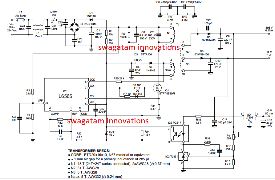
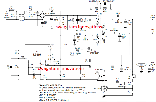
In this post I have explained how to apply the IC L6565 for making a compact multi purpose 110V, 14V, 5V SMPS circuit using minimum number of external components.
Implementing quasi-resonant ZVS flyback
The IC L6565 from ST Microelectronics is designed as a current-mode primary controller chip, to specifically suit quasi-resonant ZVS flyback converter applications. The quasi-resonant implementation is accomplished through demagnetization of a transformer sensing input, which is used for switching ON an attached power mosfet.
During the operations of this IC in a converter, the variations in the power capacity of the converter becomes compensated by a line feed forward stage acquired through the line voltage.
Circuit Diagram

Whenever the connected load is minimal or absent, the IC displays a unique feature which automatically brings down the operating frequency of the converter, and yet ensuring the operation at as far as possible around the ZVS level.
Converters using IC L6565 not only enables low consumption of the design through a low start up current, and a sustained low quiescent current, the system makes sure that it perfectly complies with Blue Angel and Energy Star SMPS guidelines.
In addition to the above explained features, the chip also includes an configurable auto disable function, an in-built current sense and shut down function, and also an accurate reference voltage input for executing basic regulation functions, and an ideal two stage overload protection.
How this 110V/14V/5V SMPS works:
In quasi-resonant SMPS circuits, the operation is implemented by synchronizing the mosfet's switch ON frequency with the demagnetization frequency of the transformer, which is generally accomplished by sensing the falling edge or the negative edge of the transformer's relevant winding voltage.
The above procedure is very simply executed by the IC L6565 through an exclusively designated pinout and using just a single resistor.
This operation enables the voltage, current variable frequency operation feature (in response to a varying input voltage current situations).
The circuit is designed to run approximately within the DCM (Discontinuous Conduction Mode) and CCM (Continuous Conduction Mode) operational mode of the transformer, which can be compared quite like a ringing self-oscillating choke converter or RCC converter.
The pin#8 which is the Vcc of the IC acquires an operating supply voltage from an external regulator network, which sets a 7V rail internally, and this voltage helps to run the entire functionality of the IC and for all the specified executions, associated with its remaining pinouts.
The IC includes an in-built bandgap circuit which enables the generation of an accurate 2.5V reference voltage for ensuring an improved regulation to the control loop used with primary feedback functionality.
You will also find an under-voltage lockout or UVLO comparator with hysteresis featured in the design, which allows the chip to shut down in case the Vcc drops below a specified voltage limit.
A zero current detection stage which is integrated within the IC becomes responsible or switching the external power mosfet in response to every negative edged pulse below the 1.6V level that's fed to this relevant pinout marked as ZCD (pin#5).
However keeping the noise immunity factor in mind and to control it effectively, the associated triggering block must get activated before pin#5 is allowed to fall below 1.6V, by enabling a +2.1V on this pinout.
This process helps the detection of the transformer demagnetization required for the quasi-resonanat operation, in which the transformer's auxiliary winding provides the required signal to the ZCD input, in addition to the IC supply.
In an alternate method where the mosfets may be intended to run in the PWM mode rather than quasi-resonanat mode, the above process can be employed for synchronizing the mosfet switch ON in response to negative pulses from an external source.
Shut Down Option
In such cases the triggering block is forced to go through momentary shut down as soon as the mosfet is switched OFF. This helps to achive a couple of objectives:
1) To ensure that the negative edged pulses following the leakage inductance demagnetization does not accidentally triggers the ZCD circuit stage, and
2) To acknowledge the functioning termed as frequency foldback.
To initiate the external mosfet at the start up, an internal starter stages i used, which enable the driver stage to execute a triggering pulse to the mosfet gate, this becomes necessary due to the absence of an initializing signal to the mosfet from the ZCD pin.
In order to keep the external component to minimum associated with auxiliary winding or a possible external clock, the voltage at the ZCD pin is enabled with a double clamping.
The upper clamp voltage is fixed at 5.2V while the lower clamping potential is rendered at one VBE over the ground level.
This enable the interface to be configured using a just one external resistor for limiting the sourced current which is furthermore shunted by the relevant pinout as per the specified values set for the internal clamping voltages.
For more info regarding the additional internal stages of this 110V, 14V and 5V rated SMPS circuit, you can refer to the original datasheet of L6565
