The 4093 is a 14-pin package containing four positive-logic, 2-input NAND Schmitt trigger gates as shown in the following figure. It is possible to operate the four NAND gates separately or collectively.
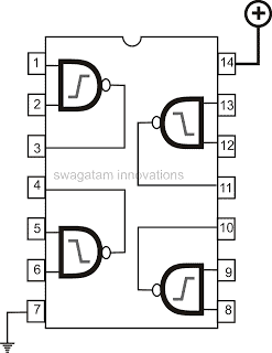
The individual logic gates of the IC 4093 works in the following manner.
As you can see each gate has two inputs (A and B) and one output. The output changes its state from maximum supply level (VDD) to 0V or vice versa depending on how the input pins are powered.
This output response can be understood from the truth table of the 4093 NAND gate, as shown below.
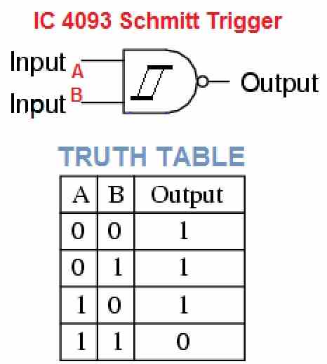
Understanding 4093 Truth Table
From the above truth table details we can interpret the logic operations of the gate as I have explained below:
- When both the inputs are low (0V), the output turns high or equal to the supply DC level (VDD).
- When input A is low (0V) and input B is high (between 3 V and VDD), the output turns high or equal to the supply DC level (VDD).
- When input B is low (0V) and input A is high (between 3 V and VDD), the output turns high or equal to the supply DC level (VDD).
- When both the inputs A and B are high (between 3 V and VDD), the output turns low (0V)
The 4093 quad NAND Schmitt Trigger's transfer characteristics are shown in the following figure. For all positive supply voltage (VDD) levels, the transfer characteristic of the gates exhibit the same basic waveform structure.
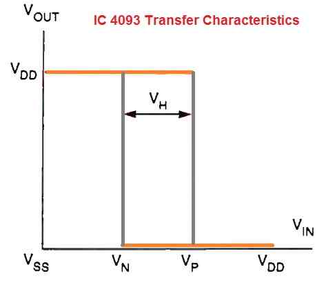
Understanding IC 4093 Schmitt Triggers and Hysteresis
One distinct feature of the IC 4093 NAND gates is, these are all Schmitt triggers. So what exactly are Schmitt triggers?
IC 4093 Schmitt triggers are a unique variety of NAND gates. One of its most useful features is how quickly they react to incoming signals.
Logic gates with Schmitt trigger will activate and turn their outputs high or low only once their input logic level reaches a genuine level. This is known as hysteresis.
The Schmitt trigger's ability to create hysteresis is a crucial feature (normally around 2.0 volts using a 10 V supply).
Let's have a quick look at the oscillator circuit depicted in Fig. A below to gain a deeper understanding of hysteresis. Figure B compares the input and output waveforms of the oscillator circuit.
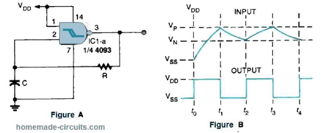
If you look at Fig. A, you'll see that the gate's pin 1 input is linked to the positive voltage rail, whereas the pin 2 input is attached to the junction of the capacitor (C) and the feedback resistor (R).
The capacitor remains discharged and the inputs and outputs of the gate are both at zero voltage (logic 0) until the supply DC is switched ON to the circuit.
As soon as the supply DC is switched ON to the oscillator circuit, pin 1 of the gate instantly goes high, although pin 2 remains low.
The NAND gate's output swings high in response to the input situation (check the time t0 in Fig. B).
As a result, the resistor R and capacitor C start charging until it reaches the level of VN. Now, Pin 2 instantly becomes high as soon as the capacitor's charge reaches the VN level.
Now since both of the gate's inputs are high (see time t1), the gate's output swings low. This forces C to discharge via R until it reaches the VN level.
When the voltage on pin#2 drops to the VN level, the gate's output swings back to high. This series of output ON/OFF cycle continues as long as the circuit remains powered. This is how the circuit oscillates.
If we look at the timing graph we find that the output turns low only when the input reaches the Vp value, and the output swings high only once the input reaches below the VN level.
This is determined by the charging and discharging of the capacitors through the time intervals t0, t1, t2, t3 etc.
From the above discussion we can see that the output of the Schmitt trigger switches only when the input reaches a well defined low level VN, and a high level Vp. This action of a Schmitt trigger to switch ON/OFF in response to well defined input voltage thresholds is called hysteresis.
One of the main advantages of the Schmitt oscillator circuit is that it automatically starts up when the circuit is powered on.
The supply voltage controls the working frequency of the circuit. This is approximately 1.2 MHz for a 12 volt supply and drops as the supply is reduced. C should have a minimal value of 100 pF, and R should not be lower than 4.7k.
IC 4093 Circuit Projects
The 4093 Schmitt trigger IC is a versatile chip which can be used for constructing many interesting circuit projects. The four Schmitt trigger gates provided inside a single 4093 chip can be customized for many useful implementations.
In this article I will elucidate a few of them. The following list provides the names of 12 interesting IC 4093 circuit projects. Each one of these will be discussed elaborately in the subsequent paragraphs.
- Simple Piezo Driver
- Automatic Street Light Circuit
- Pest Repellent Circuit
- High Power Siren Circuit
- Delay OFF Timer Circuit
- Touch Activated ON/OFF Switch Circuit
- Rain Sensor Circuit
- Lie Detector Circuit
- Signal Injector Circuit
- Fluorescent Tube Driver Circuit
- Fluorescent Tube Flasher Circuit
- Light Activated Lamp Flasher Circuit
1) Simple Piezo Driver
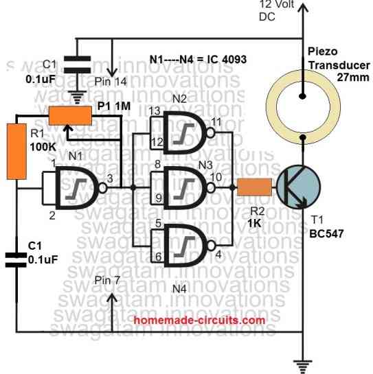
A very simple and effective piezo driver circuit can be built using a single IC 4093, as shown in the above circuit diagram.
One of the Schmitt trigger gates N1 is rigged as an adjustable oscillator circuit. The output of this oscillator is square wave with a frequency determined by the value of the capacitor C1, and the adjustment of the pot P1.
The output frequency from N1 is applied to the gates N2, N3, N4 which are connected in parallel. These parallel gates work like buffer and current amplifier stage. They together help to boost the current capacity of the output frequency.
The amplified frequency is applied to the base of BC547 transistor which further amplifies the frequency to drive an attached piezo transducer. The piezo transducer now starts buzzing relatively loudly.
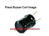
If you want increase the loudness of the piezo even further, you can try adding a 40uH buzzer coil right across the piezo wires.
2) Automatic Street Light Circuit
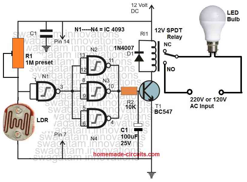
Another great use of the IC 4093 can be in the form a simple automatic street light circuit, as depicted in the above diagram.
Here, the gate N1 is hooked up like a comparator. It compares the potential generated by the resistive divider network formed by the resistance of the LDR and the resistance of the R1 pot.
In this stage the N1 effectively exploits the hysteresis feature of its in built Schmitt trigger. It makes sure that its output changes state only when the LDR resistance reaches a particular extreme level.
How it Works
During day time, when there's ample ambient light on the LDR, its resistance remains low. Depending on the setting of P1, this low resistance creates a low logic at the input pins of N1, which causes its output to remain high.
This high is applied to the inputs of the buffer stage, created by the parallel connection of N2, N3, N4.
Since all these gate are rigged as NOT gates, the output is inverted. The high logic from N1 is inverted to a low logic at the output of the N2, N3, N4 gates. This low logic or 0V reaches the base of the relay driver transistor T1 so that it remains switched OFF.
This in turn causes the relay to remain switched off with its contacts resting on the N/C contacts.
The bulb being configured at the N/O contacts of the relay remains switched OFF.
When darkness sets in, the illumination on the LDR begins decreasing, which causes its resistance to increase. Due to this, the voltage at the input of N1 starts rising. The hysteresis feature of the N1 gate "waits" until this voltage is sufficiently high to cause its output to change state from high to low.
As soon as the output of N1 becomes low, it is inverted by the N2, N3, N4 gates to create a high at their parallel outputs.
This high switches ON the transistor and the relay, and subsequently the LED bulb is also illuminated. In this way when evening or darkness sets in, the attached street light bulb is automatically switched ON.
Next morning the process reverses, and the street lamp bulb is automatically switched OFF.
3) Pest Repellent Circuit

If you are looking to build a cheap yet reasonably effectively rat or rodent repellent device, then this simple circuit might help.
Again, this design also the 4 Schmitt trigger gates from a single IC 4093.
The configuration is quite similar to piezo driver circuit, except the inclusion of the step-down transformer.
The high frequency signal which may be suitable for driving pests away is carefully adjusted using P1.
This frequency is amplified by the 3 parallel gates along and the transistor Q1. The Q1 collector can be seen configured with a primary of a 6 V transformer.
The transformer boosts the frequency to a high voltage level of 220 V or 117 V depending on the voltage spec of the transformer secondary.
This boosted voltage is applied across a piezo transducer for generating a high pitched noise. This noise can be very disturbing for the pests but may be inaudible to the humans.
The high frequency noise ultimately causes the pests to leave the area and run away to some other peaceful location.
4) High Power Siren Circuit
The figure below shows how the IC 4093 can be applied to build a powerful siren circuit. The tone of the siren is fully adjustable through a potentiometer knob.
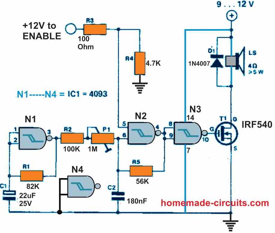
Despite its simple setup, the circuit in this example is indeed able to produce a loud sound. The n-channel MOSFET that powers the speakers enables this.
This particular MOSFET has an output drain to source resistance of just three milliohms and could be operated directly using CMOS logic circuits. Furthermore, its drain current may reach 1.7 A, with a peak drain-source voltage of 40 V.
It is fine to load the MOSFET directly with a loudspeaker because it is essentially indestructible.
Controlling the circuit is as simple as turning the ENABLE input logic high (which could be also implemented through an ordinary switch instead of a digital source).
Gate N2 oscillates as a result of the pulses from Schmitt trigger N1 once the input at pin 5 is high. Gate N2's output is fed to the MOSFET through buffer stage built around N3. The preset P1 allows N2's frequency to be modulated.
5) Delay OFF Timer with Buzzer

The IC 4093 can be also used to build a useful yet simple delay OFF timer circuit, as shown in the above figure. When power is switched ON, the piezo buzzer will start buzzing indicating that the timer is not set.
The timer is set when the push is pressed ON momentarily.
When the push button is pressed C3 quickly charges and applies a high logic at the input of the associated 4093 gate. This causes the output of the gate to turn low or 0 V. This 0 V is applied to the input of the oscillator stage built around gate N1.
This 0 V pulls the N1 gate input to 0 V via diode D1 and disables it, such that N1 is unable to oscillate.
The output of N1 now inverts the input logic zero to a logic high at its output which is fed to the parallel inputs of N2 and N3.
N2 and N3 yet again invert this logic high into logic zero at the base of the transistor, so that the transistor and the piezo remain switched OFF.
After a predetermined delay the capacitor C3 discharges fully through the R3 resistor. This causes a logic low to appear at the input of the associated gate. The output of this gate now turns high.
Due to this, the logic zero from the input of N1 is removed. Now, N1 is enabled and begins generating a high frequency output.
This frequency is further amplified by N2, N3 and the transistor to drive the piezo element. The piezo now starts buzzing indicating the delay OFF time has lapsed.
6) Touch Activated Switch
The next design shows a simple touch activated switch using a single 4093 IC. The working of the circuit can be understood with the following explanation.

As soon as power is turned on because of the capacitor C1 at N1's input, the logic at N1's input is dragged to ground voltage. This causes the N1 and N2 feedback loops to latch up with this input. This results in the creation of a 0 V logic at N2's output.
The 0 V logic makes the output relay driver stage idle during the first power switch ON.
Now imagine that the base of transistor T1 is touched with a finger. The transistor would immediately trigger ON, generating a high logic signal via C2 and D2 at the input of N1.
C2 charges quickly and prevents any subsequent erroneous activation from the touch. This ensures that the procedure is not hampered by the debouncing effect.
The above mentioned logic high immediately reverses the state of N1/N2, causing them to latch and create a positive output. The relay driving stage and the associated load are switched ON by this positive output.
Now, the next finger contact should cause the circuit to revert back to its original position. N4 is used to achieve this functionality.
Once the circuit reverts to its original status, C3 steadily charges (in few seconds), causing a logic low to appear at the appropriate input of N3.
However, the other input of N3 is already kept at logic low by the resistor R2, which is grounded. N3 is now perfectly positioned in a standby state, "ready" for the next incoming touch trigger.
7) Rain Sensor
The IC 4093 can be also perfectly configured to create a rain sensor circuit with an oscillator for the buzzer.
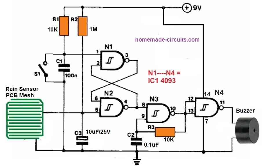
A 9 V battery may be used to power the circuit, and because of the extremely low current usage, it will survive for a year minimum. It needs to be changed after a year since it will then lack reliability due to self-discharge.
In its simplest form, the device comprises of a rain or water detector, an R-S bistable, an oscillator, and a driving stage for the warning buzzer.
A discarded 40 by 20 mm piece of circuit board serves as the water sensor. Wired connections could be used to join all tracks of the PCB. To prevent the tracks from corroding, it may be advisable to tin them.
When the power is turned on, the bistable is immediately enabled through the series network of R1 and C1.
The resistance between the two sets of tracks on the sensor PCB is really very high as long as it is dry. However, the resistance rapidly decreases when it a moisture is detected.
The sensor and resistor R2 are connected in series, and the two of them combined create a voltage divider that is moisture dependent. As soon as the input 1 of N2 becomes low, it resets the R-S bistable. Oscillator N3 is as a result turned on, and driver gate N4 operates the buzzer.
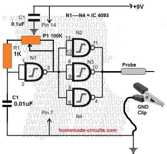
8) Lie Detector
Another great way of using the above circuit may be in the form of a lie detector.
For a lie detector, the sensing element is substituted with two pieces of wire with the ends stripped and tinned.
The person being questioned is then given the bare wires to hold tightly. The buzzer starts sounding if the target happens to tell lies. This situation is triggered due to the moisture generated on the person's grip because of nervousness and guilt.
The value of R2 determines the circuit's sensitivity; some experimentation may be required here.
By locking switch S1 ON, the oscillator (and thus, the buzzer) could be turned off.
9) Signal Injector
A 4093 IC can be effectively configured to work like an audio injector circuit. This device can be used for troubleshooting faulty parts in audio circuit stages.
If you've ever attempted to fix your own sound systems, you may be fully familiar with the capabilities of a signal injector.
A signal injector, for the layperson, is a basic square-wave generator created to pump an audio frequency into a circuit under test.
It can be used to detect and identify a faulty component in a circuit. A signal injector circuit can also be used to investigate the RF sections of AM/FM receivers.
The figure above depicts a schematic representation of the Signal Injector. The oscillator or square-wave generator section of the circuit is structured around a single gate (IC1a).
The values of capacitor C1 and resistor R1/P1 set the frequency of the oscillator, which can be around 1 kHz. By adjusting the P1 and C1 values for the oscillator stage, the circuit's frequency range could be changed.
The circuit's square-wave output switches ON/OFF across the entire supply voltage rail. Supply voltages varying from 6 to 15 volts could be used to power the circuit.
However, you can also use a 9V battery. The output of gate N1 is interconnected in series with the remaining three gates of the IC 4093. These 3 gates can be seen connected in parallel with each other.
With this arrangement, the oscillator output is adequately buffered and amplified to a level that can suitably feed the circuit which is being tested.
How to use a Signal Injector
To troubleshoot a circuit using an injector, the signal is injected across components from back to front. Let's say you want to troubleshoot an AM radio with an injector. You begin by applying the injector's frequency to the base of the output transistor.
If the transistor and the other parts that follows it are working properly, the signal will be heard through the speaker. In case no signal is audible, the injector signal is carried forward towards the speaker until a sound is produced by the speaker.
The part immediately preceding this point could be assumed most likely to be faulty.
10) Fluorescent Tube Driver
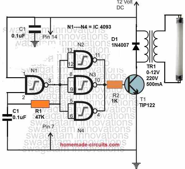
The figure above depicts the Fluorescent-Light Inverter's schematic design using the IC 4093. The circuit may be used to power a fluorescent bulb using two 6 volt rechargeable batteries or a 12-volt automotive battery.
With a few small adjustments, this circuit is practically identical to the previous one.
In its existing format, Q1 is alternately switched from saturation and cut-off using the buffered oscillator output.
The primary of T1 experiences a rising and falling magnetic field as a result of the collector switching of Q1, which is linked to one terminal of a step-up transformer.
As a result, the secondary winding of T1 experiences an induction of a substantially larger fluctuating voltage.
The fluorescent tube receives the voltage created in T1's secondary, which causes it to light up promptly and without flickering.
A 6 watt fluorescent tube may be driven by the circuit using a 12-volt supply. When employing two 6 volt rechargeable wet batteries, the circuit consumes just 500 mA.
Therefore several hours of operation could be achieved from a single charging. The lamp will work considerably differently than when powered by 117 volts or 220V of AC mains.
No starter or preheater is required since the tube is energized with high-voltage oscillations. The output transistor must be installed on a heatsink while constructing the circuit. The transformer can be quite small with a 220V or 120V primary and a 12.6-volt, 450 mA secondary.
11) Fluorescent Flasher
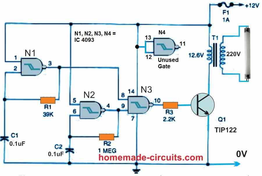
The Fluorescent Flasher, depicted in figure above, incorporates stages from both the fundamental 4093 oscillator circuit and the 4093 fluorescent-light driver circuit.
This design, consisting of two oscillators and an amplifier/buffer stage, could be implemented as a flashing warning light for vehicles. As can be seen, here, one pinout of the amplifier/buffer stage N3, connects with the output of the first oscillator (N1).
The second oscillator built around N2 provides the input to the amplifier's other leg (N3). The two oscillators independent RC networks define their operating frequencies. With the help of transistor Q1, the system generates a frequency-modulated switching output.
This switching output induces a high-voltage pulse in the secondary winding of transformer T1. Its output only becomes low as soon as both signals supplied to IC1c are high. This low shuts off Q1 and eventually, the lamp starts to flash.
12) Light Activated Lamp Flasher
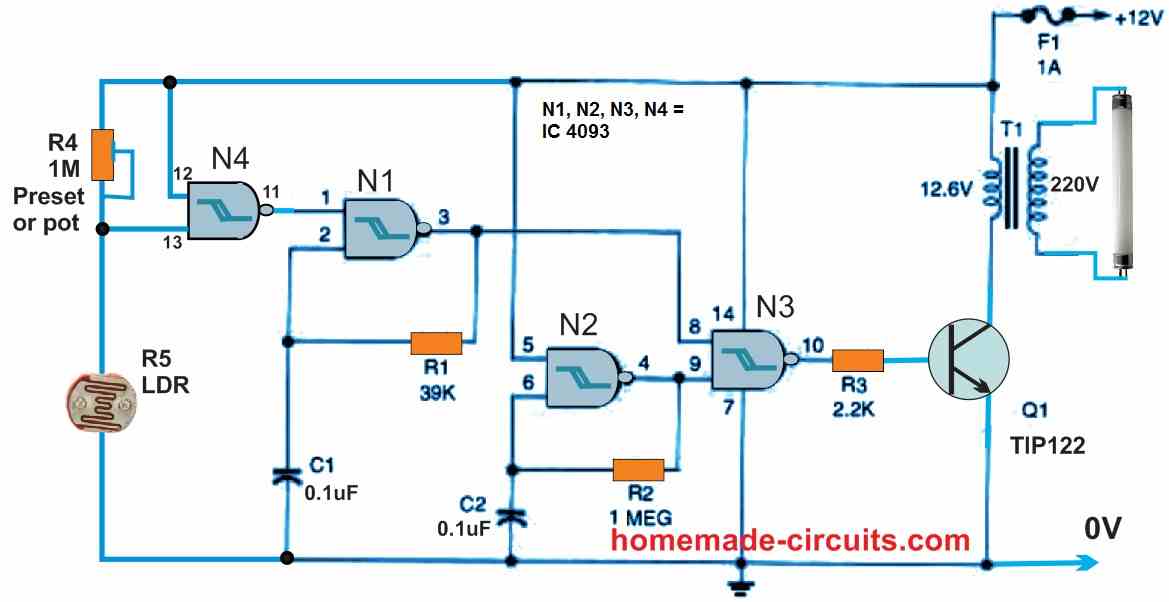
The Light-Triggered Fluorescent Flasher as shown above is an upgrade to the previous IC 4093 fluorescent flasher circuit. The previous 4093 flasher circuit has been reconfigured to instantly start flickering as soon as an approaching motorist illuminates the LDR with its headlamps.
An LDR, R5, serves as the light sensor in the circuit. Potentiometer R4 adjusts the circuit's sensitivity. This must be tweaked such that when a light beam is flashed over the LDR from a distance of 10 to 12 feet, the fluorescent lamp begins to flash.
Additionally, potentiometer R1 is adjusted to ensure that when the light source is removed from the LDR, the flasher shuts off on its own.