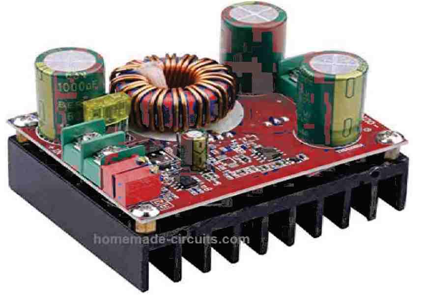
In this post I have explained how to build a simple 12 V to 19 V boost converter circuit which can used to charge a 19 V battery from a 12 V car battery.
The main application of this circuit could be for the charging of a laptop battery from a car battery,
How the Circuit Works
The 12 V to 19 V converter circuit diagram can be seen in the following figure.
The working principle is actually very straightforward.
A free-running astable oscillator is employed to operate a voltage doubler circuit.
A series pass transistor is used to regulate the output voltage, which is controlled by a comparator. The earth connections for the input and output lines is the same and is common with the negative of the 12 V supply source.
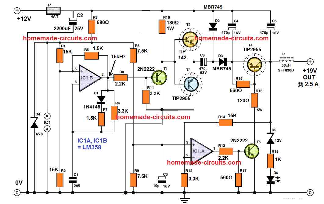
IC1B becomes the main active part of the the astable multivibrator configuration. Capacitor C1 and resistor R4 which are connected across the feedback path provide a working frequency of 15 kHz roughly.
Diode D1 and resistor R7 make sure that the square wave output operates with a 50:50 duty cycle.
C1 capacitor must be a good quality capacitor with high stability and low temperature coefficient features, a ceramic type capacitor should do the job well.
The dode D1 should be rated with a temperature characteristics so that the output square wave is maintained correctly all the time regardless of the output load conditions and circuit heating.
Transistors T2 and T3 gets switched alternately through the square waves generated by the IC1B.
When T3 is in the switched ON period, capacitor C3 charges up to 12 V by means of D2. Next, while the T3 goes into the switched OFF period, causes T2 to turn ON, which enables the negative terminal of C3 to be instantly linked with the +12 V supply.
However, in this situation the charge stored inside in C3 is unable to change immediately, therefore as soon as the C3 negative terminal gets linked with the high 12 V potential, it becomes necessary for its positive terminal to also step up.
The situation causes the C3 positive terminal to get ‘boosted up’ to approximately two times the supply voltage.
In real life operation , due to the losses occurring through the diodes and transistors essentially mean that the output cannot be exactly two times the supply input level, rather will be a slightly below the expected 2X level.
Schottky diodes are employed in the circuit to ensure that the forward voltage drop is kept to the minimum. D3 is used for rectifying the voltage and C4 is configured to store the rectified output from the diode.
Make sure to use very high quality capacitor for C3 since it will be solely responsible for delivering the entire output current to the load. The regulation for the output voltage is executed by op-amp IC1A.
The potential divider created by the resistors R14 and R12 detects the T4 collector voltage and then IC1A compares it with the reference voltage generated from the network comprising of the parts R6, R9 and zener diode D4.
The level of the stepped up 19 V output can be fixed by adjusting the value of R14. A 15 kΩ value for R14 will provide an approximate output voltage of 19 V.
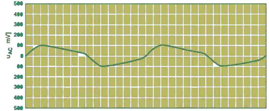
The ripple voltage content of the 19 V output at full load will be as shown in the next figure.
If the capacitor value C6 is increased, will ensure that the reference voltage goes up at a very slow rate when power is first switched ON. This feature can provide this 12 V to 19 v converter circuit a nice soft-start or slow-start characteristic. This switch-on delay can be verified by looking at the LED D6.
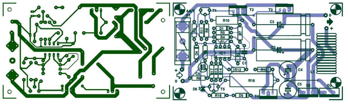
PCB Design
The complete PCB design and the components overlay diagrsm is shown in the following image: