In this post I will comprehensively discuss a 2 simple 12V 2 amp SMPS circuit using the IC UC2842. We study a 2 amp flyback design by evaluating various formulas, which provides the exact selection details for the transformer winding and the parts specifications.
Design#1: Introduction
The first design is based on the versatile IC VIPer53-E.
The VIPer53-E is built with an improved current mode PWM controller which has a high voltage MDMesh™ Power MOSFET within the very same package. The VIPer53-E can be found in a couple of distinct packages, DIP8 and PowerSO-10.The benchmark board is undoubtedly an offline wide range power supply which includes the VIPer53-E designed for secondary regulation by operating the PWM controller via an opto-coupler. The switching frequency is 100 kHz and the overall output power is 24 W.
Below given are a few of the the main features of the IC:
• SMPS based general purpose power supply
• Current mode control along with variable limiting facility
• Efficiency around a good 75%
• Output is safeguarded with a short-circuit and overload protection
• Over temperature is also controlled through a in-built Thermal shutdown protection
• Complies with EN55022 Class B EMI specification and Blue Angel standards.
The circuit diagram of the proposed 12V 2 amp circuit using VIPer53-E could be witnessed in the below shown image:
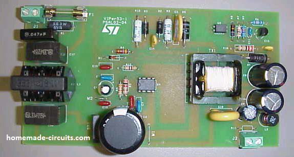
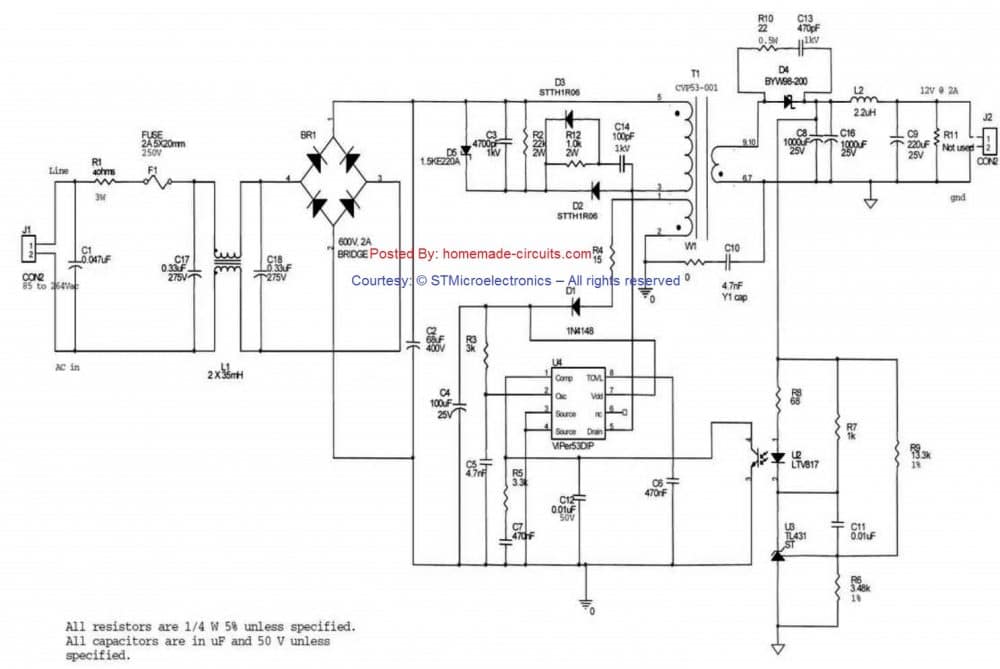
DOWNLOAD COMPLETE PCB AND PARTS LIST
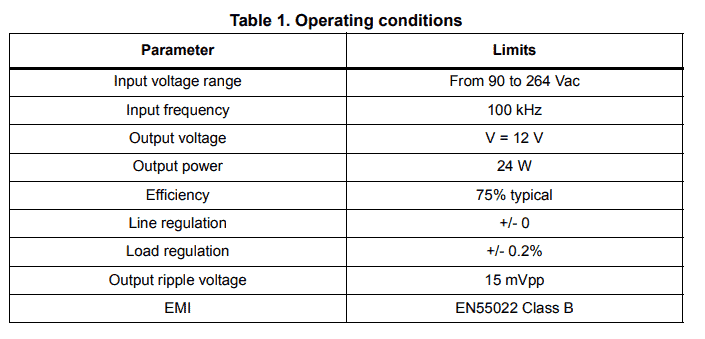
Main Operating Conditions can be studied through the following image:
Transformer Details:
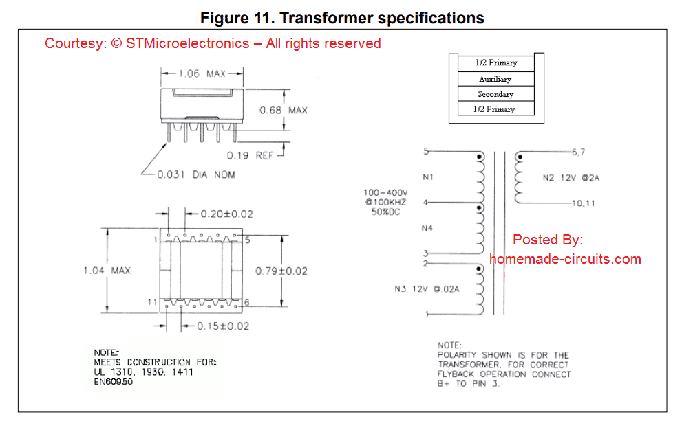
The ferrite core transformer winding details for the above SMPS circuit could be analyzed as per the data furnished in the following figure:
More Info on VIPer53-E can be studied in this article
Design#2: Introduction
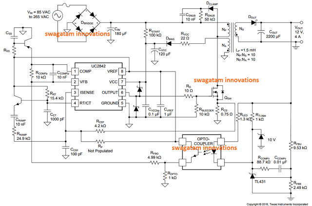
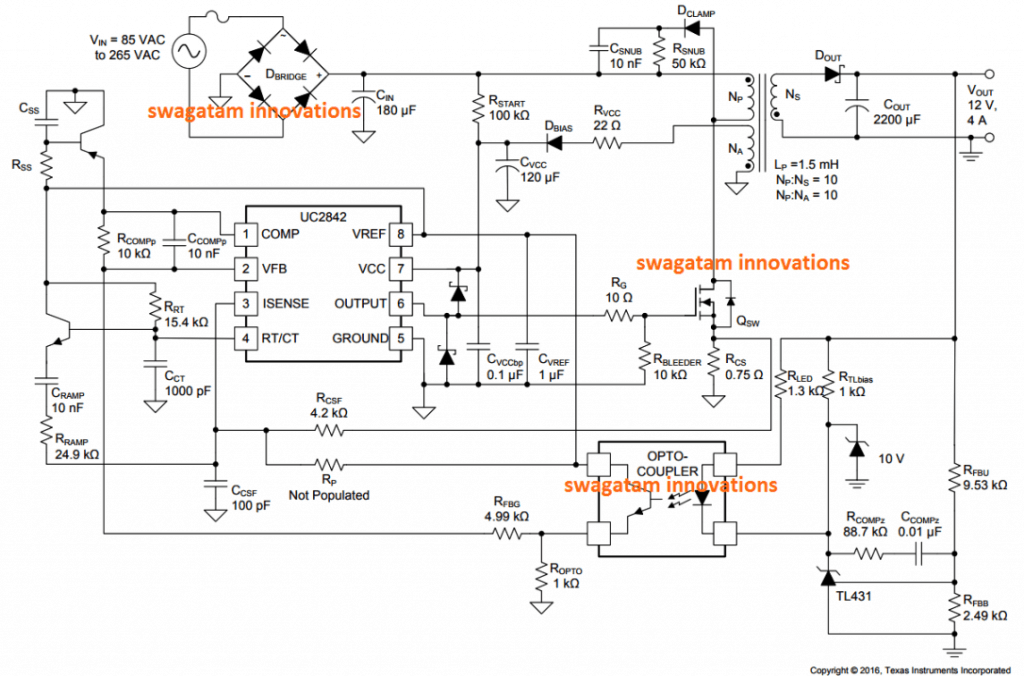
The next design is based on the IC UC2842 from Texas Instruments, which can be also used for building a high grade, solid state, very reliable SMPS circuit rated at 12V, and with a current output @ 2 amp to 4 amps.
The complete circuit diagram of this design can be sen in the following figure:
Let’s try to understand the functions and criticalities of a few of the main components used in this 12V 2 amp SMPS circuit:
Cin Input Bulk capacitor and minimum bulk voltage:
The shown bulk capacitor Cin may be incorporated using a single or a few capacitors in parallel, possibly by using an inductor across them to eliminate noise generated due to differential-mode conduction. The value of this capacitor decides the level of minimum bulk voltage.
If a lower value Cin is used to reduce minimum bulk voltage, might result in raised primary peak current overloading the switching mosfets and also the transformer.
On the contrary keeping the value larger might result in higher peak current on the mosfet and the trafo, which is also not acceptable, therefore a reasonable value as indicated in the diagram should be chosen.
It may be done by using the following formula:

Here Vin(min) indicate the RMS value of the minimum AC input voltage which is around 85 V RMS.
fLINE(min)denotes the frequency of the above RMS value which may be assumed to be 47Hz.
With reference to the above equation, in order to achieve a minimum of 75V bulk voltage value, at 85% efficiency, the Cin value will need to be around 126uF, in our prototype 180uF was found to be just fine.
Calculating the Tansformer turn ratios:
To begin with the transformer turn calculation, the most favorable switching frequency needs to be found out.
Although the IC UC2842 is specified to produce a maximum frequency of 500kHz, considering all the feasible and efficiency related parameters it was decided to select and set the device at around 110kHz.
This allowed the design to be reasonably well balanced in terms of the transformer size, EMI filter dimension and still keep the operations within the tolerable losses.
The term Nps refers to the primary of the transformer and this may be determined depending upon the rating of the driver mosfet used along with the rating of the secondary rectifier diode specifications.
For an optimal mosfet rating we first need to calculate the peak bulk voltage with reference to the maximum RMS voltage value which is 265V input AC in our case. Therefore we have:

For the sake of simplicity and cost effectiveness, a 650V rated mosfet IRFB9N65A was selected for this 12V 2 amp smps circuit prototype.
If we consider the maximum voltage stress on the mosfet drain to be around 80% of its specifications, and taking 30% as the permissible voltage spike from the maximum bulk input supply, the resultant reflected output voltage can be expected to be lower than 130V as expressed in the following equation:

Therefore for a 12V output the maximum primary/secondary transformer turn ratio or the NPS may be calculated as indicated in the following equation:

In our design a turn ratio of Nps = 10 has been incorporated.
This winding must calculated in such a way that it is able to produce a voltage that may be a little higher than the minimum Vcc specification of the IC, so that the IC is able to operate under optimal conditions and stability is maintained throughout the circuit.
The auxiliary winding Npa can be calculated as shown in the following formula:

The auxiliary winding in the transformer is used for biasing and providing the operating supply to the IC.
Now for the output diode, the voltage stress on it may be equivalent to the output voltage and the reflected input supply, as given below:

In order to counter the voltage spikes due to “ringing” phenomenon, a Schottky diode rated with a blocking voltage of 60V or higher was felt necessary and employed in this design.
Also to keep away high voltage current spike factor, this flyback converter is designed to work with a continuous conduction mode (CCM).
Calculating the Maximum Duty Cycle:
As discussed in the above paragraph, once we calculate the NPS of the transformer, the required maximum duty cycle Dmax can be calculated through the transfer function as allocated for CCM based converters, the details can eb witnessed below:

Transformer Inductance and Peak Current
In our discussed 12V 2 amp smps circuit the transformer magnetizing inductance Lp was determined as per the CCM parameters. In this example the inductance was chosen such that the converter is able to get into the CCM working zone with around 10% load and using minimum bulk voltage in order to keep the output ripple to the lowest.

For more details regarding the various technical specifications and formulas you can study the original datasheet here
