In this post I have explained the complete building procedure of a 2-meter amateur ham radio transmitter circuit, using ordinary electronic components and ordinary test equipment.
What is 2-Meter VHF Radio
The 2-meter amateur radio band is a section of the VHF radio spectrum, which includes frequencies ranging from 144 MHz to 148 MHz in International Telecommunication Union region (ITU) Regions 2 (North and South America plus Hawaii) and 3 (Asia and Oceania) and from 144 MHz to 146 MHz in ITU Region 1 (Europe, Africa, and Russia).
The authorization rights of amateur radio users incorporate the utilization of frequencies in this particular band for telecommunication locally, typically within around a 100 miles (160 km) range.
Main Features
This 2 m transmitter dumps around a 1.5 watts into the aerial, works using a 12 V battery, is frequency modulated, and could be controlled through a crystal or VFO.
Specific consideration has been given towards greater purity of the signal spectrum which is accurately changed to ensure that the harmonics are much reduced below 45 dB.
The input audio can be supplied either from a crystal or dynamic microphone, and the output could be used with a correctly matched 50 to 75 feet aerial.
Additionally it could be momentarily controlled into an unrestricted SWR load, which is short or open circuit, without any damage to the output transistor. Furthermore, being phase modulation changed into frequency modulation, the chances of over-deviation is almost negligible.
FM may be accomplished through a couple of techniques. The easiest being the utilization of a varicap diode over the crystal or VFO. This technique requires a tiny supplemental circuitry, but involves the negative aspect of the probability of over-deviation, that may be over ± 2.5k Hz.
The next technique is through the creation of a constant carrier frequency that is subsequently phase modulated and converted into FM by trimming of the AF response.
Phase modulation leads to a rise in deviation not just through amplitude but also through increasing AF causing the audio amplifier to get a falling characteristic.
The advantages are that over-deviation is practically out of the question, deviation is uniform and even, resolution on simple slope detection is quite easily compared to absolute FM. Therefore phase modulation had been implemented for this 2-meter transmitter circuit.
Phase modulation demands a lower fundamental frequency when ample deviation is desired at 144 MHz to 146 MHz, and that's exactly why 8.0 to 8.1 MHz had been picked, which can work with a 18x multiplier chain to achieve the intended working frequency.
Standard 2-meter amateur band transmitters make use of BJTs working in class C in the multiplier stages, however these include significant drawbacks. The input impedance is incredibly small, and these are current dependent rather than voltage.
This results in higher consumption through the preceding circuit stage, which makes it necessary for the preceding stage to be exactly matched if the Q of the stage is required to be maintained, and the amplification of undesired harmonics eliminated.
Although much less efficient, FET's are able to defeat these issues, since they run comfortably in the class C, causing harmonic generation at lower currents and due to the fact that high input impedance devices feature voltage dependent operation.
As a result the Q is taken care of, undesired harmonics covered up, however offering limited amplification across the desired frequency ranges. The output from the multiplier is an additional FET which works with 10 to 20 mA serving a standard driver and power amplifier.
Modulator Circuit
A higher input impedance is actually supplied by Tr1 and C1 as shown in Fig. 1 although not crucial, it helps isolating the microphone while R1 and C2 act like an RF filter, with the TR1 gate grounded by R2.

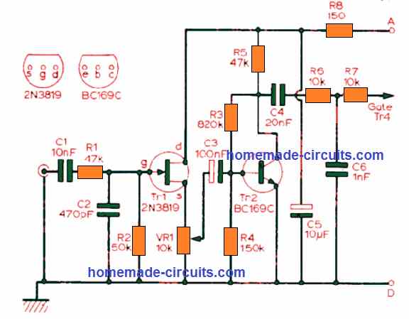
This resistor isn't significant and just about any value above 50 k will be enough. Tr1 works like an impedance modifier providing current amplification only, which may include around 30% voltage loss.
VR1 attached to the Tr1 source adjusts the audio output and therefore the deviation, by following the source of TR1 towards the Tr2 base through C3.
Tr2 produces voltage gain, and by integrating the upper bias chain with the its collector, some level of feedback is achieved, which restricts the gain to around 100 times.
R8 and C5 function as a decoupling network for the modulator towards the power supply side and R7, while C6 holds RF away from the modulator output. R6 and C4 provide the some additional trimming to the circuit to accomplish the necessary falling characteristic to the audio results. The current requirement for the modulator is approximately 500 µA.
Crystal Oscillator, VFO Amplifier, Phase Modulator
Power applied to all these stages are stabilized through D1 and R13 Fig. 2. The oscillator stage is a Pierce oscillator circuit, where the crystal can be seen hooked up in between the gate and drain terminals of TR3, to ensure that removing the crystal allows the gate to be open for the VFO attachment whenever Tr3 is required to work as an amplifier.
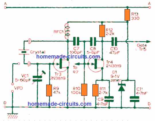
VC1 is positioned to drag the crystal to a particular frequency and does not cause any effect on the VFO. RFC1 inhibits the signal from passing to Tr3, by allowing it to pass through C7 towards the TR4 gate, which is the phase modulator, having R12 as the load.
The output passes by means of C10 towards the multiplier chain, and the feedback passes via C8 generating the phase modulation. The audio signal is given to the TR3 gate, 1V p/p being the minimum requirement by the phase modulator.
Multiplier Chain
Transistors Tr5, Tr6 and Tr7 in Fig. 3, are configured tripler and doubler stages respectively.
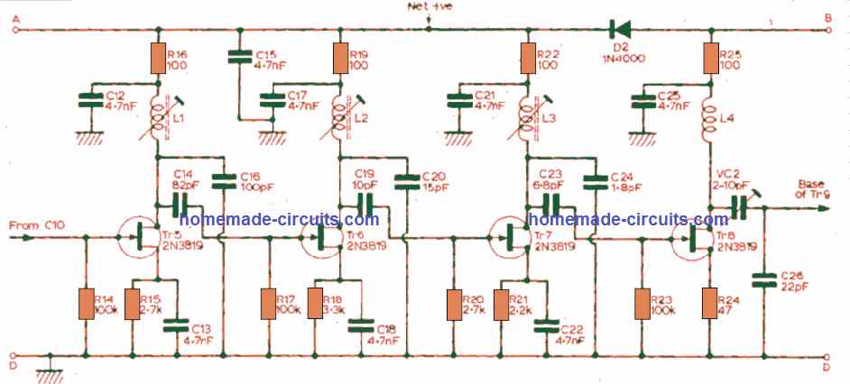
These stages are designed with similar layouts, and are used to resonate on the harmonic frequencies. All these identical stages operate with quiescent currents of around 500 µA.
If this is increased to 1.5 mA with an RF signal connected, they begin working in Class AB mode. Since the FETs provide high input impedance, the output could be extracted from the drain, which helps to avoid the use tapping on the coils.
Since the loading is supposed to be negligible, this allows the circuit Q to remain high and ensures that tuning of the coils is not very complex.
The tuning for the output of the power amplifier is over a sharp range. Therefore, VC2 needs to be very meticulously adjusted to get the finest results.
A tiny metal shielding is essential around L4, to stop feedback from reaching L3, which may otherwise result in induced oscillation, negatively affecting the efficiency of the stage.
R24 works like a current limiter and voltage feedback generator for Tr8.
Driver and Power Amplifier
All these stages are designed to run in the class C mode.
The Tr9 input as shown in, Fig. 4, is tuned through L4, VC2 and C26. The VC2 and C26 allow impedance matching for the TR9 base of Tr9. RFC2 provides the DC return path.
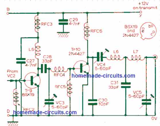
The overall dissipation from the transistor Tr9 using a properly set multiplier chain and a dynamic crystal attached, could be up to 300 mW which means a little heat sink may be required to be installed with this transistor.
Tr10 must be mounted on the track side of the PCB. Its input impedance is really low and capacitive in nature.
The C28 and VC3, are used for tuning L5 and create an impedance matching into the base of TR10. RFC4 helps to compensate for the input capacity and RFC5 acts like the DC return path.
Seeing that Tr10 may dissipate up to 2.5 Watts of power, a large heat sink may be required to keep this power transistor cool.
RFC6 is positioned to suppress RF to ensure that the output circuit configuration using VC4, C30, L6, C31, L7 and VC5 solely becomes the collector load for TR10. The screening shield put around L7 and VC5 helps to inhibit the output harmonic content significantly, and one should make sure this is included at all costs.
How to Build
The circuit is best built over a double-sided copper clad PCB, Fig. 5. It is advisable that all the assembly related instructions are implemented with precise care. See that every earth point is delivered to the upper area of the PCB.
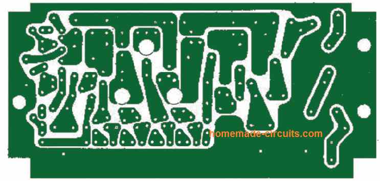
All component leads are inserted up to the neck and kept as small as it can be, while the extended legs of coils and resistors must be appropriately grounded. The coils must be built with the help of the recommended drill shafts,
After the winding on the drill is done, the coil should be forced over the stiff former, then the space between the turns must be adjusted by stretching exactly to the recommended overall length of the coil.,
Finally, the coils must be secured in place over the formers by applying a very mild layer of epoxy resin adhesive.
Coils that are recommended to have adjustable iron slugs must be secured in the set position with the help of a melted wax drop.
All the top end holes of these coils must be countersunk, using a appropriate drill bit.
Construction is commenced first by fixing the PCB inside the die-cast container and drilling the bolting holes through the board and the base.
Next begin assembling the components by soldering as shown in Fig. 6, from the long axis outwards.
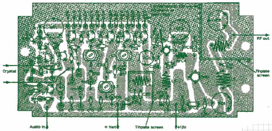
First solder the screens into position before everything to facilitate easy installation. Additionally it may be a good idea to flip the PCB over, bolt it to the cover of the box, then drill holes through the center of the variable capacitors and coils with a No.60 drill.
These holes must be further made bigger to 6 mm to enable easy access to the respective trimmers during the final tuning process, after the PCB is installed inside the boxed.
The heatsink for the Tr10 can be any standard type available in the market, but for Tr9 this could be built manually by turning a 12 mm square of copper or tinplate with the help 5 mm drill mandrel and then pushing it around the transistor.
How to Set up
Clean the solder assembly with ethyl alcohol, and then examine the PCB soldering cautiously and see if there are any dry solder or shorted solder bridges.
Next, before fixing it into the case, hook up the wires temporarily and plug in the crystal into the slot. Use an ammeter or any current meter and connect it in series with the positive of the supply line, along with a series 470 ohm resistor. After this, hook up a 50 to 75 Ohm shielded dummy load at the output via a good power meter.
How to Test
Without attaching a crystal, connect the 12V supply and make sure the current intake is no higher than 15 mA, to the audio stage, oscillator, phase modulator, zener and quiescent multiplier stage.
If the meter indicates higher than 15 mA, then there may be some fault in the layout or maybe Tr8 is not stable and oscillating. This can be best identified with the help of a RF "sniffer" device placed close to L4, and the problem corrected by appropriately adjusting VC2.
Once the above condition is verified, pay attention to the modulator and employing a high impedance meter, verify that the Tr2 collector voltage reads half the supply voltage with reference to the supply end of R19.
If you find this to be higher than 50%, try an increased value of R4 until the recommended reading is achieved, or conversely, if the reading is lower than 1/2 the supply, decrease the value of R4.
To get even better optimization, an oscilloscope can be used to tweak the C6 value until a 3dB voltage with 3kHz is obtained, compared a 1 kHz response. This may be considered equivalent to the most effective roll off and a good frequency modulation. This test should be made across base/emitter of TR4.
After this, connect a crystal and check the current response, you must see some increase in the current consumption. However, to safeguard the output transistor from high dissipation, this current consumption must be adjusted by setting VC4 and VC5 appropriately.
In the next step, to ensure that our 2 m transmitter works with the right harmonics, the multiplier stage should be optimized by adjusting the core slugs of all the variable inductors to get maximum output on the "sniffer" device. Alternatively, the same may be implemented by optimizing for maximum current, which corresponds to the correct harmonic optimization for the circuit stage.
The trimmer VC2 could be adjusted by using a sharp plastic pointed object, to fix the circuit with optimum current consumption.
After this, fine-tune trimmer VC3 which may slightly effect the VC2 setting, and therefore VC2 might need to be readjusted again. Next, adjust VC4 and VC5 until you see the best possible RF output, with minimum possible total current consumption.
After this, it may be required to repeat this alignment and fine-tuning process for all the variable capacitors, effecting each other, until an optimal adjustment is achieved across the trimmers with maximum RF output.
The ultimate tweaking must result in an average output wattage of 0.75 and 1 W into the dummy load with a overall current consumption of approximately 300 mA.
In case you have an access to an SWR meter, you can connect the circuit to an aerial with an input crystal on a dead frequency and then refine the tuning through VC4 and VC5 until an optimum RF output is measured, corresponding to a minimum SWR reading.
After all these set ups are completed, testing with an input audio modulation should not cause any change in the RF output level. After a few more confirmations, when a fully satisfactory performance is accomplished from the 2 meter transmitter circuit, the board may be installed in the selected enclosure or the die-cast box, and further tested to make sure everything is fine with the working of the unit as previously confirmed.
Parts List
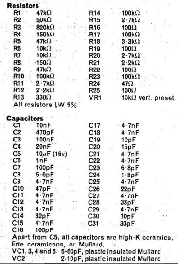
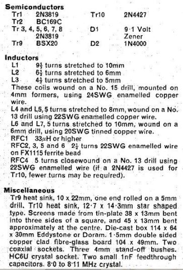
Where is the microphone connection? I assume it’s fed with 12v? Where is the antenna connection? Where do you wire in for ctcss?
MIC output or an audio frequency can be applied to C1 in the first circuit. You can use any voltage between 6V and 12V for the MIC. MIC circuit is not shown in the article. Instead of MIC you can feed an audio signal to C1 for testing purpose. Antenna is connected across VC5 in the last schematic. I don’t know about CTCSS.
I wonder how swagatam managed to give a reply or answer to all querries!
nice post!
Hi
Can you please explain what is meant in the construction of the inductors: 6 1/2 turns stretched to 6mm
Hi, it means a closely wound coil having 6 and a half turns, pulled and stretched to 6 mm length.
Physically stretched? Does that not damage the wire?
Yes physically stretched, it is an usual method of fine tuning RF coils. A copper coil cannot get damaged unless tampered intentionally.
Thank you I didn’t know that.
Are these plans available anywhere in usable format? The schematic and board layout all have “homemade-circuits” over the top of them that makes them unusable without significant effort to remove that.
A useful project for budding hams, who wants to come on air soon after getting a license. Will be more useful if a frequency readout is incorporated. Otherwise how to know at what frequency you are transmitting.
Thanks for the feedback, you are correct, this can be probably done by checking the frequency response of the transmitter over a nearby 2 meter receiver, and then marking the dial of the variable capacitor with the corresponding frequency value.