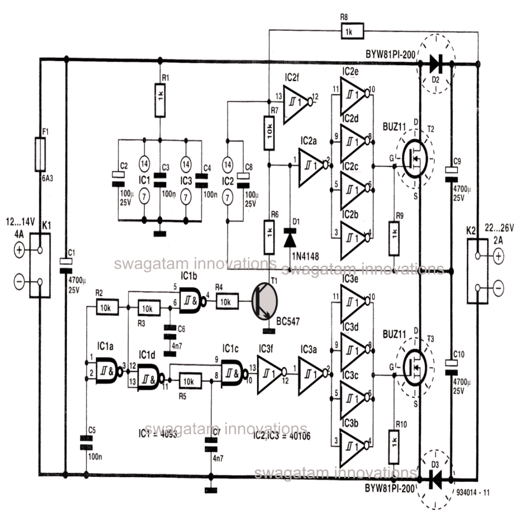
In this post I have explained a voltage high current doubler circuit which will almost double the voltage that's been applied at the input (up to 15V max), and also it becomes specifically useful since it allows higher current loads to be used at the output, in the order 10 amps.
Since the voltage doubler circuit explained here is able to handle high current loads, the design becomes ideally applicable for raising solar panel voltages when there's no adequate amount of sun light incident on the panels.
Circuit Operation
Looking at the given circuit diagram, let's assume we apply a 12V at the input of the circuit, the output would generate a potential of around 22V.
The circuit initiates its functioning when IC1a, R2 and C2 starts generating rectangular waves.
This signal also reaches at the output of IC1d, albeit in an inverted mode.
The presence of R2, C2 delays the output of IC1a which causes the output of IC1b to attain less than 0.5 duty factor, resulting in a waveform where the negative half may be shorter than the positive half).
The above also becomes true at the output of IC1c, were the input data is delayed with the help of C7, R5.
The output from IC1c which is in an inverted form is further buffered thrice via IC3f, IC3a and the gates in parallel IC3b-----IC3c.
The output from the above is finally used for driving the power mosfets.
The transistor T1 is driven from the output of IC1b..... when T1 is ON, the point between R6, R7 attains a 2V potential, however since IC2a requires a 11 to 22V input, the negative potential for this chip is plucked from the positive of the input voltage, because the supply voltage and the collector of T1 is already subjected with the doubled voltage.
D1 is introduced to guarantee that the input to IC2a never drops below 10.5 V.
During the conduction periods of T1, T2 and T3 conduct alternately.
When T2 is switched ON, C10 gets charged with voltage equal to the input supply voltage through T3 and D3.
When T2 is turned OFF, and T3 gets ON, C9 goes through identical process as C10 above. However C10 holds the charge due to the presence of D3 which stops it from discharging.
Because the two capacitors are in series, the net voltage now attains a level that's almost twice that of the applied input voltage.
One interesting thing here is, since the circuit involves many inverting stages and also a few delay networks, the output mosfets can NEVER conduct together which makes the circuit extremely safe with the operations.
C1 buffers the input applied voltage in order to load the input with constant power irrespective of the varying current parameters across the output.
The components which are marked with dashed circles need to be appropriately cooled by adding large heatsinks to them.


With over 50,000 comments answered so far, this is the only electronics website dedicated to solving all your circuit-related problems. If you’re stuck on a circuit, please leave your question in the comment box, and I will try to solve it ASAP!