In this post I have explained the pinout function and other important specifications of the IC 4043. I have explained about the complete datasheet of this very interesting chip.
Pinout Datasheet of IC 4043
Technically the IC 4043 is a quad set/reset (R/S) latch with 3 logic state output.
To be more precise this chip has 4 sets of inputs (meaning 8 input pinouts) and 4 corresponding single outputs.
The 4 sets of inputs consist of 4 pairs of set/reset inputs.
For every set/reset we have one corresponding output.
All these set reset inputs respond to high logic signals, creating a bistable effect at their corresponding output pinouts.
Bistable Flip/Flop
Bistable refers to flip flop action, in other words a high pulse to the "set" input makes the corresponding output high from its original low state, and a high to the reset input reverts the above state from high back to low state.
Therefore basically to make a corresponding outputs high, we need to apply a high on their "set" inputs and to make the outputs low again we simply need to apply another high to their reset inputs.
The functioning of the input and output pinouts are as simple as that.
In addition to this, the IC has another interesting input pinout OE which is a common output enable pinout.
Set/Reset Function
For enabling the above explained set/reset actions in the IC, this OE input should be connected with logic high or simply with Vdd (supply votage).
In the above situation the output is allowed with the specified flip flop functioning.
If the OE input is connected with ground, the output freezes and produces a high impedance response, that is neither shows a low output nor a high, rather locks input a unresponsive blocked state, hence the name 3 logic state output.
Thus the OE input can be used to shut down the IC functioning if required for a particular application.
The IC works best with supply voltages from 5 to 15V.

Let's summarize the input output pinout functions and specifications of the IC 4043 with the following data:
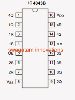
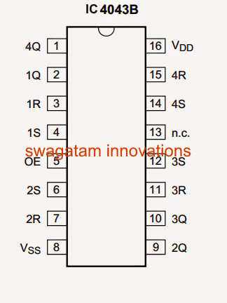
- 1Q to 4Q (Pins: 2, 9, 10, 1) 3-state buffered latch output
- 1R to 4R (Pins: 3, 7, 11, 15) reset input (active HIGH)
- 1S to 4S (Pins: 4, 6, 12, 14) set input (active HIGH)
- OE (Pin:5) common output enable input
- VSS (Pin: 8) ground supply voltage
- N.C. (Pin: 13) not connected
- VDD (Pin: 16) supply voltage
More Updates:
In this posts I have explained the working of the IC 4043 and IC 4044 by studying the various specifications, datasheet of the devices and their pinout arrangement.
Basically both the variants are quad cross-coupled CMOS 3-state R/S or Reset/Set Latches. Quad means having 4 outputs which can be set or latched with a logic high through a control input signal, or reset to logic zero by a subsequent input signal.
The 3-state feature allows the ICs to be controlled using 3 logic
The basic working principle of IC 4043 and IC 4044 is the same as above, the only difference being, IC 4043B are quad cross-coupled 3-state NOR Latch, and IC 4044B are quad cross-coupled 3-state NAND Latch.
Pinout Diagram
The following pinouts diagrams of the ICs show the internal structure and pinout details of the devices:


In the diagrams above we can see that each of the types has 4 latches with one output and 2 individual RESET/SET inputs. The function of the ENABLE pin for all the SET/RESET inputs is identical.
A logic HIGH at the ENABLE pin allows the latch states to get connected with the relevant outputs, a logic low or 0 disconnects the latch states from their outputs causing a complete open circuit across the outputs.
NOR Latch, NAND Latch Equivalent Logic Diagrams
The following diagrams show the equivalent latches in the form of NOR and NAND latches, which are present inside each of the 4 latches of the individual ICs.

As we can see, each of the latch blocks are controlled using 3 logic control inputs, namely SET, RESET, and ENABLE, therefore the output is dependent on these 3 input states. The truth table for these 3 logic states can be learned from the following diagram:

In the above truth table, the full-form of the various abbreviated symbolic alphabets can be understood as given below: S = SET Pin R = RESET Pin E = ENABLE Pin Q = OUTPUT Pin OC = Open Circuit NC = No Change
Main Features of the IC 4043, and IC 4044 are summarized below:

Practical Basic Working Simulation of the SET/RESET and ENABLE Pins

Working Description
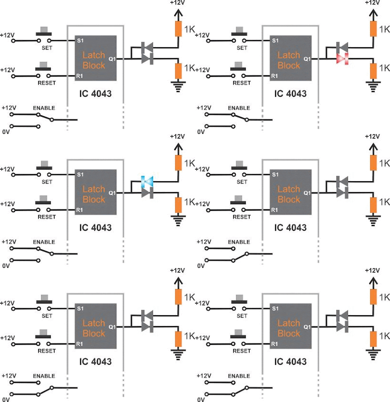
From the above simulation GIF we can understand the working of the quad latch modules with the following points:
When the SET is pin applied with a positive supply, the output goes high and becomes latched even if the positive potential is removed from SET pin, as indicated by the red LED (forward biased).
When the RESET pin is applied with a positive pulse, the latch breaks, and the output goes LOW permanently even if the positive is removed from the RESET pin. This is indicated by the illumination of the blue LED.
The above operations can be implemented only as long as the ENABLE pin of the IC is at a positive supply potential. When attached to a negative or ground potential, the output of the latch becomes open and unresponsive to the SET/RESET operations.


With over 50,000 comments answered so far, this is the only electronics website dedicated to solving all your circuit-related problems. If you’re stuck on a circuit, please leave your question in the comment box, and I will try to solve it ASAP!