The proposed solar optimizer circuit can be used for getting the maximum possible output in terms of current and voltage from a solar panel, in response to the varying sun light conditions.
A couple of simple yet effective solar panel optimizer charger circuit are explained in this post. The first one can be built using a couple of 555 ICs and a few other linear components, the second optin is even simpler and uses very ordinary ICs like LM338 and op amp IC 741. I have explained the procedures.
Circuit Objective
As we all know, acquiring highest efficiency from any form of power supply becomes feasible if the procedure doesn't involve shunting the power supply voltage, meaning we want to acquire the particular required lower level of voltage, and maximum current for the load which is being operated without disturbing the source voltage level, and without generating heat.
Briefly, a concerned solar optimizer should allow its output with maximum required current, any lower level of required voltage yet making sure the voltage level across the panel stays unaffected.
One method which is discussed here involves PWM technique which may be considered one of the optimal methods to date.
We should be thankful to this little genius called the IC 555 which makes all difficult concepts look so easy.
Using IC 555 for the PWM Conversion
In this concept too we incorporate, and heavily depend on a couple of IC 555s for the required implementation.
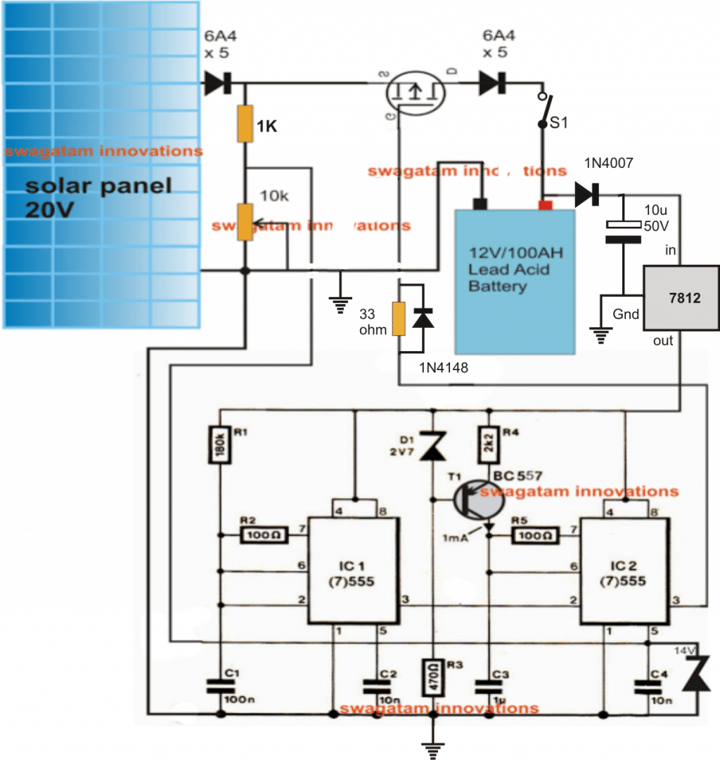
Looking at the given circuit diagram we see that the entire design is basically divided into two stages.
The upper voltage regulator stage and the lower PWM generator stage.
The upper stage consists of a p-channel mosfet which is positioned as a switch and responds to the applied PWM info at its gate.
The lower stage is a PWM generator stage. A couple of 555 ICs are configured for the proposed actions.
How the Circuit Functions
IC1 is responsible for producing the required square waves which is processed by the constant current triangle wave generator comprising T1 and the associated components.
This triangular wave is applied to IC2 for processing into the required PWMs.
However the PWM spacing from IC2 depends on the voltage level at its pin#5, which is derived from a resistive network across the panel via the 1K resistor and the 10K preset.
The voltage between this network is directly proportional to the varying panel volts.
During peak voltages the PWMs become wider and vice versa.
The above PWMs are applied to the mosfet gate which conducts and provides the required voltage to the connected battery.
As discussed previously, during peak sunshine the panel generates higher level of voltage, higher voltage means IC2 generating wider PWMs, which in turn keeps the mosfe switched OFF for longer periods or switched ON for relatively shorter periods, corresponding to an average voltage value that might be just around 14.4V across the battery terminals.
When the sun shine deteriorates, the PWMs get proportionately narrowly spaced allowing the mosfet to conduct more so that the average current and voltage across the battery tends to remain at the optimal values.
The 10K preset should be adjusted for getting around 14.4V across the output terminals under bright sunshine.
The results may be monitored under different sun light conditions.
The proposed solar panel optimizer circuit ensures a stable charging of the battery, without affecting or shunting the panel voltage which also results in lower heat generation.
Note: The connected soar panel should be able to generate 50% more voltage than the connected battery at peak sunshine. The current should be 1/5th of the battery AH rating.
How to Set up the Circuit
- It may be done in the following manner:
- Initially keep S1 switched OFF.
- Expose the panel to peak sunshine, and adjust the preset to get the required optimal charging voltage across the mosfet drain diode output and ground.
- The circuit is all set now.
- Once this is done, switch ON S1, the battery will start getting charged in the best possible optimized mode.
Adding a Current Control Feature
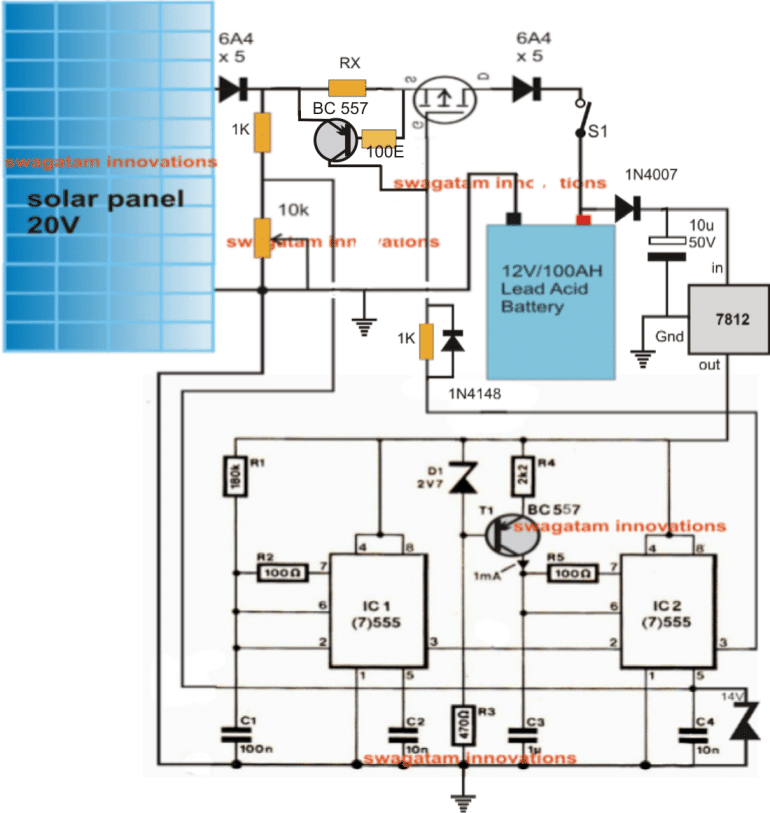
A careful investigation of the above circuit shows that as the mosfet tries to compensate the falling panel voltage level, it allows the battery to draw more current from the panel, which affects the panel voltage dropping it further down inducing a run-away situation, this may seriously hinder the optimizing process
A current control feature as shown in the following diagram takes care of this problem and prohibits the battery from drawing excessive current beyond the specified limits. This in turn helps to keep the panel voltage unaffected.
RX which is the current limiting resistor can be calculated with the help of the following formula:
RX = 0.6/I, where I is the specified minimum charging current for the connected battery
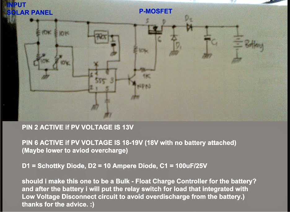
A crude but simpler version of the above explained design may be built as suggested by Mr. Dhyaksa using pin2 and pin6 threshold detection of the IC555, the entire diagram may be witnessed below:
No Optimization without a Buck Converter
The above explained design works using a basic PWM concept which automatically adjusted the PWM of a 555 based circuit in response to the changing sun intensity.
Although the output from this circuit produces a self adjusting response in order to maintain a constant average voltage at the output, the peak voltage is never adjusted making it considerably dangerous for charging Li-ion or Lipo type batteries.
Moreover the above circuit is not equipped to convert the excess voltage from the panel into a proportional amount of current for the connected lower voltage rated load.
Adding a Buck Converter
I tried to rectify this condition by adding a buck converter stage to the above design, and could produce an optimization that looked very similar to an MPPT circuit.
However even with this improved circuit I could not be entirely convinced regarding whether or not the circuit was truly capable of producing a constant voltage with trimmed down peak level and a boosted current in response to the various sun intensity levels.
In order to be entirely confident regarding the concept and to eliminate all the confusions I had to go through an exhaustive study regarding buck converters and the involved relation between the input/output voltages, current, and the PWM ratios (duty cycle), which inspired me to create the following related articles:
Calculating Voltage, Current in a Buck Inductor
The concluding formulas obtained from the above two articles helped to clarify all the doubts and finally I could be perfectly confident with my previously proposed solar optimizer circuit using a buck converter circuit.
Analyzing PWM Duty Cycle Condition for the Design
The fundamental formula which made things distinctly clear can be seen below:
Vout = DVin
Here V(in) is the input voltage which comes from the panel, Vout is the desired output voltage from the buck converter and D is the duty cycle.
From the equation it becomes evident that the Vout can be simply tailored by "either" controlling the duty cycle of the buck converter or the Vin....or in other words the Vin and the duty cycle parameters are directly proportionate and influence each others values linearly.
In fact the terms are extremely linear which makes the dimensioning of an solar optimizer circuit much easier using a buck converter circuit.
It implies that when Vin is much higher (@ peak sunshine) than the load specs, the IC 555 processor can make the PWMs proportionately narrower (or broader for P-device) and influence the Vout to remain at the desired level, and conversely as the sun diminishes, the processor can broaden (or narrow for P-device) the PWMs again to ensure that the output voltage is maintained at the specified constant level.
Evaluating the PWM Implementation through a Practical Example
We can prove the above by solving the given formula:
Let's assume the peak panel voltage V(in) to be 24V
and the PWM to be consisting a 0.5 sec ON time, and 0.5sec OFF time
Duty cycle = Transistor On time / Pulse ON+OFF time = T(on) / 0.5 + 0.5 sec
Duty cycle = T(on) / 1
Therefore substituting the above in the below given formula we get,
V(out) = V(in) x T(on)
14 = 24 x T(on)
where 14 is the assumed required output voltage,
therefore,
T(on) = 14/24 = 0.58 seconds
This gives us the transistor ON time which needs to be set for the circuit during peak sunshine for producing the required 14v at the output.
How it Works
Once the above is set, the rest could be left for the IC 555 to process for the expected self-adjusting T(on) periods in response to the diminishing sunshine.
Now as the sunshine diminishes, the above ON time would be increased (or decreased for P-device) proportionately by the circuit in a linear fashion for ensuring a constant 14V, until the panel voltage truly falls down to 14V, when the circuit could just shut down the procedures.
The current (amp) parameter can be also assumed to be self adjusting, that is always trying to achieve the (VxI) product constant throughout the optimization process. This is because a buck converter is always supposed to convert the high voltage input into a proportionately increased current level at the output.
Still if you are interested to be entirely confirmed regarding the results, you may refer to the following article for the relevant formulas:
Calculating Voltage, Current in a Buck Inductor
Now let's see how the final circuit designed by me looks like, from the following info:
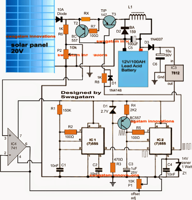
As you can see in the above diagram, the basic diagram is identical to the earlier self optimizing solar charger circuit, except the inclusion of IC4 which is configured as a voltage follower and is replaced in place of the BC547 emitter follower stage. This is done in order to provide a better response for the IC2 pin#5 control pinout from the panel.
Summarizing the Basic Functioning of the Solar Optimizer
The functioning may be revised as given under:IC1 generates a square wave frequency at about 10kHz which could be increased to 20kHz by altering the value of C1.
This frequency is fed to pin2 of IC2 for manufacturing fast switching triangle waves at pin#7 with the help of T1/C3.
The panel voltage is suitably adjusted by P2 and fed to the IC4 voltage follower stage for feeding the pin#5 of the IC2.
This potential at pin#5 of IC2 from the panel is compared by pin#7 fast triangle waves for creating the correspondingly dimensioned PWM data at pin#3 of IC2.
At peak sun shine P2 is appropriately adjusted such that IC2 generates the broadest possible PWMs and as the sun shine begins diminishing, the PWMs proportionately gets narrower.
The above effect is fed to the base of a PNP BJT for inverting the response across the attached buck converter stage.
Implies that, at peak sunshine, the broader PWMs force the PNP device to conduct scantily {reduced T(on) time period}, causing narrower waveforms to reach the buck inductor...but since the panel voltage is high, the input voltage level {V(in)} reaching the buck inductor is equal to the panel voltage level.
Thus in this situation, the buck converter with the help of the correctly calculated T(on) and the V(in) is able to produce the correct required output voltage for the load, which could be much lower than the panel voltage, but at a proportionately boosted current (amp) level.
Now as the sun shine drops, the PWMs also become narrower, allowing the PNP T(on) to increase proportionately, which in turn helps the buck inductor to compensate for the diminishing sunshine by raising the output voltage proportionately...the current (amp) factor now gets reduced proportionately in the course of the action, making sure that the output consistency is perfectly maintained, by the buck converter.
T2 along with the associated components form the current limiting stage or the error amplifier stage. It makes sure that the output load is never allowed to consume anything above the rated specs of the design, so that the system is never rattled and the solar panel performance is never allowed to divert from its high efficiency zone.
C5 is shown as a 100uF capacitor, however for an improved outcome this might be increased to 2200uF value, because higher values will ensure better ripple current control and smoother voltage for the load.
P1 is for adjusting/correcting the offset voltage of the opamp output, such that pin#5 is able to receive a perfect zero volts in the absence of a solar panel voltage or when the solar panel voltage is below the load voltage specs.
The L1 specification may be approximately determined with the help of the info provided in the following article:
How to Calculate Inductors in SMPS Circuits
Solar Optimizer using Op Amps
Another very simple yet effective solar optimizer circuit can be made by employing a LM338 IC and a few opamps.
So I have explained the proposed circuit (solar optimizer) with the help of the following points:The figure shows an LM338 voltage regulator circuit which has a current control feature also in the form of the transistor BC547 connected across adjustment and ground pin of the IC.
Opamps Used as Comparators
The two opamps are configured as comparators. In fact many such stages may be incorporated for enhancing the effects.
In the present design A1's pin#3 preset is adjusted such that the output of A1 goes high when the sun shine intensity over the panel is about 20% less than the peak value.
Similarly, A2 stage is adjusted such that its output goes high when the sunshine is about 50% less than the peak value.
When A1 output goes high, RL#1 triggers connecting R2 in line with the circuit, disconnecting R1.
Initially at peak sun shine, R1 whose value is selected a lot lower, allows maximum current to reach the battery.
Circuit Diagram
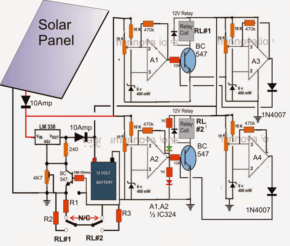
When sunshine drops, voltage of the panel also drops and now we cannot afford to draw heavy current from the panel because that would bring down the voltage below 12V which might entirely stop the charging process.
Relay Changeover for Current Optimization
Therefore as explained above A1 comes into action and disconnects R1 and connects R2. R2 is selected at a higher value and allows only limited amount current to the battery such that the solar voltage does not crash below 15 vots, a level that's imperatively required at the input of LM338.
When the sunshine falls below the second set threshold, A2 activates RL#2 which in turn switches R3 to make the current to the battery even lower making sure that the voltage at the input of the LM338 never drops below 15V, yet the charging rate to the battery is always maintained to the nearest optimum levels.
If the opamp stages are increased with more number of relays and subsequent current control actions, the unit can be optimized with even better efficiency.
The above procedure charge the battery rapidly at high current during peak sunshines and lowers the current as the sun intensity over the panel drops, and correspondingly supplies the battery with the correct rated current such that the it gets fully charged at the end of the day.
What Happens with a Battery Which may not be Discharged?
Suppose in case the battery is not optimally discharged in order to go through the above process the next morning, the situation may be fatal to the battery, because the initial high current might have negative affects over the battery because it's yet to discharged to the specified ratings.
To check the above issue, a couple of more opamps are introduced, A3, A4, which monitor the voltage level of the battery and initiate the same actions as done by A1, A2, so that the current to the battery is optimized with respect to the voltage or the charge level present with the battery during that period of time.
hello everyone, sir
i’ have a 180-volt battery bank and a 392-volt PV bank what diagram should I use to make an adequate MPPT charge controller?
Hello Gad,
an MPPT can be unnecessarily complex and costly, instead I would recommend using a buck converter, whose performance will be as good as an MPPT.
Yazılarınız hayranlıkla izliyorum bu sayede oldukça bilgi sahibi oldum sizden 48 v güneş paneli için nasıl bir devre kurabiliriz yardımlarınız için teşekkür ediyorum
You are most welcome, Glad you found the articles helpful…
Hey Swagatam,
Thanks for sharing the details regarding the solar panels MPPT optimization. I’m in design phase of the home solar project. I needs to check the I,V of each panel (for that i’m using INA219 sensor). Then the generated energy must be transferred to the central PCB to decide btw the load and charging Lead acid battery. As the produced energy would be much higher and can’t be sent normally, should i use the buck converter at each panel plate?
How would you combine the energy of all the panels in parallel?
Thanks
Thank you Aashir, for posting this interesting question!
Yes, definitely a buck converter is the best way to optimize the excess voltage from a solar panel. You can terminate the outputs of the buck converters through schottky diodes and join the output from these diodes in parallel. In this way the power from the all solar panels will be combined into a single output.
Thanks for explaining. So i added the LM2575-5.0BU voltage regulator and connected all panels in parallel with the diode at output as per your suggestion (12V panels). Can you please guide me further on how to transfer this combined output-generated energy to the central PCB (which is separate) and then to load or batteries by means of a (2-pin connector and wires) or any other expert advice? Also, for the 5 parallel load units please recommend a relay bearing coming energy (5 solar panels and 5 wind units).
Thanks in advance.
OK that sounds good, however since I do not know regarding the central PCB details it can difficult for me to suggest regarding the configuration.
Also, for the relay transfer please provide more information, how do you want to switch the loads across the solar and the wind sources??
Basically, its 5 different PCB’s (one for wind, solar, batteries, load and the central PCB to manage the generated energy and shift it to load OR batteries if load is not connected.) Energy generated both from solar and wind should be shifted to central PCB (combine the generated energy or make separate please suggest) and then central PCB should decide to either shift it to load if load is attached Or to the batteries (no load). There are 5 different loads connected in parallel. Earlier i was using a 5 pin switch but i need to replace it with a relay. Please suggest your expert advice. Thanks
Thanks for updating the info.
It may be a good idea to combine the wind and the solar power together through a buck converter and individual diodes.
A relay changeover stage might not be required. Instead we can use a battery over discharge detector which can cut off the battery from the load when it happens to get discharged below a critical level.
In a normal situation, both the renewable sources and the battery together supplies their power to the load. The battery is also charged concurrently by the renewable sources.
However, in case the battery gets discharged below a critical it is simply cut-off from the load until it is fully charged again.
Nevertheless the loads keep getting the power from the renewable sources, and the battery is also simultaneously charged.
Thanks for your quick response. Can you please share an example of discharge detector for me? Also, to combine the solar and wind energy into one source, can we add them up in Series to get high current and voltage? Thanks
Combining the solar and the wind power must be in parallel, not in series. Here’s the complete circuit diagram as shown below. I forgot to include the buck converters. The buck converters will come in between the solar panel and its schottky diode and between the windmill output and its schottky diode.
" rel="ugc">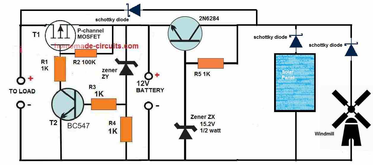
For the solar panels of 5V, 250mA what should be buck convertor output like 5V or 3.3V as for the 5V output buck convertor seems odd. My second question related to it would be why we need to use the buck convertor with the diode as it means we are losing the other produced energy? Please consider my silly questions. Thanks
I did not know that your solar panel is a small 5V 250 mA, I assumed it to be somewhere around 36V 5 ampere.
For a 5V 250mA there’s no need of any buck converter, and no need of the diodes.
I think the buck converter requirement was suggested by you in your initial comment.
Thanks for your detailed explanation. One last thing if you don’t mind, can you please share the discharge critical level of batteries. Where it’s happening in circuit and what’s the critical level you set? Is it by firmware? Excuse me for the vague questions I’m trying to learn it. Thanks
The critical discharge level is handled by the zener diode ZY, the BC547 BJT, and the P-MOSFET. As long as the battery voltage is above the ZY breakdown level, it remains conductive and provides the biasing voltage to the BC547, so the BC547 remains switched ON, which in turn allows the P-MOSFET to remain switched ON and this allows the battery supply to the load.
As soon as the battery voltage drops below the ZY breakdown level, ZY stops conducting, turning OFF the BC547 and the MOSFET, thereby cutting off the battery supply to the load.
More info can be found in the following article:
https://www.homemade-circuits.com/battery-deep-discharge-protection-circuit/
Hey Swagatam, me again and just looking at some of these designs while wondering how you would modify section for switching current from panel to battery using MoSfet instead of say TIP147? I like the buck boost part in the circuit using the 2×7555’s and the 741 as a Vfollower. Also wondering what freq you figure this PWM operates at on the output of 2nd timer? Have you constructed this design or is it still in CAD? I have 4x 25 w panels I want to build small controllers for to connect as maintenance. controllers to keep vehicle batteries up. The panels are only 25w so they wouldn’t be heavy current circuits. I was just thinking MoSfets would be little more efficient on loses from R.
Hi Bret, You can replace the BJT with a Pchannel Mosfet, however a MOSFET will require a minimum of 9V peak to operate optimally, whereas a BJT can operate right from 1 V onward.
I have not tested the PWM response on the buck converter but the two IC555 stages are well tested for the PWM generation.
For your small solar controllers I would rather recommend using a buck converter such as the XL4015, which are highly reliable, customizable and powerful.
https://www.homemade-circuits.com/modifying-xl4015-buck-converter-with-an-adjustable-current-limiter/
hi there,
I tried to edit my response to your previous comment but the system said “no” 🙂
I’ve found a recent paper on PV DC optimizer circuits…. https://www.researchgate.net/publication/308928331_Performance_Analysis_of_Solar_Power_Optimizer_for_DC_Distribution_System/download I wonder if this might be of interest
Yes, the idea is good but the full schematic is not provided.
hi there!
I’m considering installing a PV array, where the panels will be subjected to intermittent and ultimately total shade for the array. I have a MPPT and a single inverter. Will these optimizers suit the purpose of ‘isolating’ the shaded panel?
Thanks
Doug
Hi,
MPPT (Maximum Power Point Tracking) is a technology used in solar inverters to optimize the output power of a photovoltaic (PV) system. MPPT can help to mitigate the effect of partial shading on a PV array, but it may not completely eliminate the issue.
However, if the shading is severe and covers a large portion of the array, even MPPT may not be able to completely eliminate the issue. In such cases, it may be necessary to consider alternative solutions such as reconfiguring the system to use microinverters or DC optimizers, which can isolate the shaded panels from the rest of the array and allow them to operate independently.
thanks so much for responding. Actually, I’m looking toward the DC optimizer approach. As I understand it, these serve to reduce the impact of a shaded panel in either a series or parallel arrangement from degrading the array output. I wondered if you “solar optimizer” circuit is, in fact a “DC Optimizer”? If not, do you have such a design that effectively can be added to each panel that is in the array?
You are correct in your understanding of the DC optimizer approach. DC optimizers are electronic devices that are used in photovoltaic (PV) systems to mitigate the impact of shading on PV panels.
However, unfortunately I do not have any such design which can solve the issue you are facing.
The above designed might not work for the intended application.
Can you tell me how exactly your solar panels are connected, in series or in parallel? If they are in parallel then optimization can be much easier, and we can install buck converters for each panel for optimizing their outputs individually.
Again, thank you for replying!
Since the MPPT charger will handle a 30v input (and the pv panels are 30v (for 60 cell panels), I suppose parallel strings would work just fine. Would the optimizers need to be “buck” or “boost” ie to lift falling voltage with shaded cell strings on certain panels. (ie 20v per string on a 3 string diode bypassed 60cell PV Panel).
I guess the advantage with higher voltages would be lower current carrying conductors. Is that correct?
Buck boost both can be used which can switch depending upon the shading level of the panels, however, although a boost converter would boost the voltage, the current would drop significantly. It will actually depend on the battery charging voltage specification, if it is well below the lowest voltage from the shaded panel then the boost converter may not be required.
Yes as the voltage specification is increased the current specification can go down, and vice versa.
I’m going to make a guess that of these designs, your favorite is the one with the 741 voltage follower using the buck boost? I’m thinking about constructing some circuits to implement for keeping stationary car batteries up using small 10w ~ panels in a window.
Yes the 741 version looks good, however it is an old design and there are probably easier alternatives which I can suggest today. I won’t recommend a buck boost type rather only a buck converter type.
I doubt think the 10 watt panels would be sufficient to keep the relatively large car batteries topped-up, nevertheless you can give it a try and let us know the results.
Please sir about the first design am confused calculating the number of turn for inductor (L1) even after reading the provided article for the calculations. Please can you kindly help with the inductor value (inductance)? Thanks
Gody, the calculations for a buck converter coil and design can be studied in the following article:
https://www.homemade-circuits.com/dc-to-dc-converter-circuits-using-sg3524-buck-boost-designs/
and the same circuit can be applied for solar charger also, no need of going with the above explained complex procedures.
Since solar power optimizers are in effect mppt controllers at the panel level, for an off grid installation with battery banks, why shouldn’t a cheaper PWM charge controller be a less expensive and just as good as a MPPT charge controller? Also, the value, it seems to me in having power optimizers, is it would allow mismatched solar panels to be used. For a single 12v panel which might have an operating voltage of 17v to 21 v on a sunny day, that voltage might drop to a voltage below the voltage needed by the charge controller which is approximately 5 volts over the charging voltage for a 12v battery. Having two panels connected in series would ensure that the voltage would rise above the threshold needed by the charge controller even on a cloudy day. Also a “power optimizer” that was a SEPIC dc controller that did boost or buck conditioning of the panel voltage to a useable battery charging voltage for a charge controller would seem to be advantageous even with a single panel in allowing additional battery charging time for cloudy
Yes you are right! MPPT is not always necessary, and a simple linear regulator based charger or at the most a buck converter charger is more than enough for charging a battery efficiently through solar panels.
great, I am a foreign student doing research on this topic, could you please tell me how to calculate and choose the control circuit for voltage stabilizer and current regulator? teach me how to draw basic current and voltage curves of load and semiconductor valves (Ud, Id, iv, Uv)
Hello, I appreciate your interest and curiosity, however, the questions that you have asked cannot be explained in short through comments, you will have learn them stage wise by going through the relevant articles, and through many practical experimentations, and with trial and error
Can I have some references, please?
Please specify your exact circuit need, I’ll try to provide you the references…
The circuit uses 2 ic555, ic4741, ic7812, I want to know more about the principle of the circuit, can you teach me and documentation about ic4741
The IC4741 seems to be obsolete and there’s no information about it anywhere on the internet….so I can’t figure out its working.
Can you show me how it works?
thank you sir for your reply . I want to design the solar optimizer circuit for li ion battery having rating of 12 v 7 Ah, so how to design the circuit for solar charger circuit for li ion battery ?
Hi Shashank, a buck converter is probably the best solar circuit that can provide you with an optimized charging output. You can try the following design
LM317 Variable Switch Mode Power Supply (SMPS)
make sure to adjust the output to slightly lower voltage than the actual full charge level of the battery. Ans use a 24 V 1 Amp solar panel.
Sir in one design of Self Optimizing Solar Battery Charger Circuit you have used p channel mosfet and in the above design you have used pnp transistor TIP147 so it would give same result ?
you have also made one more change by using opamp IC4 741 while in other design you have used transistor , so is there any difference in using two different components op amp and transistor in the circuit ?
Shashank, all the shown circuits work with slightly different principles but there basic job is to ensure that the solar panel is utilized with maximum efficiency.
Hi Swagatam,
Thanks for the reply i will build the given circuit and let you know the result.
Thanks & Regards
Anandan
Hi Swagatam,
First would like to thank for the above circuit.
I am planning to built this ckt but have little confusion on part of preset alignment.
I got solar panel of rated voltage 17v and of 25w, battery is 12v 7ah using this battery and solar panel as of now for testing only
Can u please explain about the all 4 preset alignment like for A1 & A2 on what voltage it should be set and once it is done then on what voltage the A3 & A4 preset should be set?
Thanks & Regards.
Anandan
Thanks Anandan,
I would recommend the following design instead of the above for your application:
https://www.homemade-circuits.com/2012/10/make-this-3-step-automatic-battery.html
It's much easier with identical features.
The transformer will need to be replaced with the solar input, the rest is explained in the article itself.
If you have further questions feel free to ask them.