A boost converter (also called step-up converter) is a DC to DC converter circuit which is designed to convert an input DC voltage into an output DC voltage with a level that may be much higher than the input voltage level.
However the process always conserves the relation P = I x V, which means that as the output of the converter steps up the input voltage, the output proportionately undergoes a reduction in current, which causes the output power to be almost always equal to the input power or less than the input power.
How a Boost Converter Works
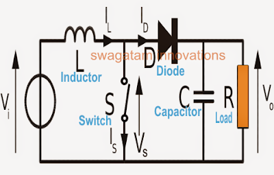
A boost converter is a kind of SMPS or switch mode power supply which fundamentally works with two active semiconductors (transistor and diode) and with a minimum of one passive component in the form of a capacitor or an inductor or both for greater efficiency.
The inductor here basically is used for stepping up the voltage and the capacitor is introduced for filtering the switching fluctuations and for reducing current ripples at the output of the converter.
The input power supply which may be required to be boosted or stepped up could be acquired from any suitable DC source such as batteries, solar panels, motor based generators etc.
Operating Principle
The inductor in a boost converter plays the important of stepping up the input voltage.
The crucial aspect which becomes responsible for activating the boost voltage from an inductor is due to its inherent property of resisting or opposing a suddenly induced current across it, and due to its response to this with a creation of magnetic field and subsequently destroying of the magnetic field. The destroying leads to the releasing of the stored energy.
This above process results in the storing of the current in the inductor and kicking back this stored current across the output in the form of back EMF.
A relay transistor driver circuit can be considered a great example of a boost converter circuit. The flyback diode connected across the relay is introduced to short circuit the reverse back EMFs from the relay coil and to protect the transistor whenever it switches OFF.
If this diode is removed and a diode capacitor rectifier is connected across the transistor's collector/emitter, the boosted voltage from the relay coil can be collected across this capacitor.

The process in a boost converter design results in an output voltage that’s always higher than the input voltage.
Boost Converter Configuration
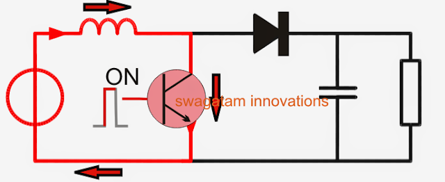
Referring to the following figure, we can see a standard boost converter configuration, the working pattern may be understood as given under:
When the shown device (which could be any standard power BJT or a mosfet) is switched ON, current from the input supply enters the inductor and flows clockwise through the transistor to complete the cycle at the negative end of the input supply.

During the above process the inductor experiences a sudden introduction of current across itself and tries to resist the influx, which results in the storing of some amount of the current in it through the generation of a magnetic field.
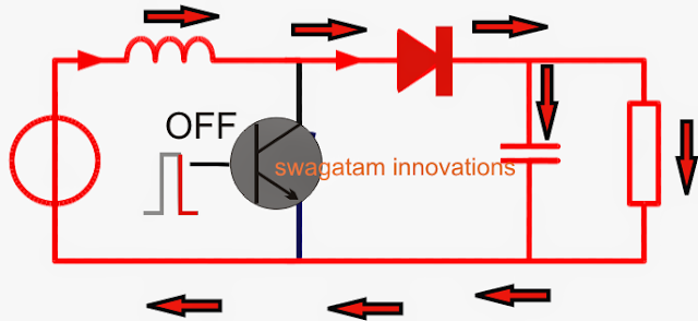
At the next subsequent sequence, when the transistor is switched OFF, the conduction of current breaks, yet again forcing a sudden change in the current level across the inductor. The inductor responds to this by kicking back or releasing the stored current. Since the transistor is in the OFF position, this energy finds its path through the diode D and across the shown output terminals in the form of a back EMF voltage.

The inductor performs this by destroying the magnetic field which was earlier created in it while the transistor was in the switch ON mode.
However, the above process of releasing energy is implemented with an opposite polarity, such that the input supply voltage now becomes in series with the inductor back emf voltage. And as we all know that when supply sources join in series their net voltage adds up to produce a bigger combined outcome.
The same happens in a boost converter during the inductor discharge mode, producing an output which may be the combined result of the inductor back EMF voltage and the existing supply voltage, as shown the diagram above
This combined voltage results in a boosted output or a stepped up output which finds its path through the diode D and the across capacitor C to ultimately reach the connected load.
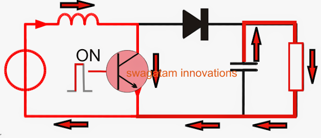
The capacitor C plays quite an important role here, during the inductor discharge mode the capacitor C stores the released combined energy in it, and during the next phase when the transistor switches OFF again and the inductor is in the storing mode, the capacitor C tries to maintain the equilibrium by supplying its own stored energy to the load. See the figure below.

This ensures a relatively steady voltage for the connected load which is able to acquire power during both the ON, and OFF periods of the transistor.
If C is not included then this feature is cancelled resulting in a lower power for the load and lower efficiency rate.
The above explained process continues as the transistor is switched ON/OFF at a given frequency, sustaining the boost conversion effect.
Modes of Operation
A boost converter may be primarily operated in two modes: the continuous mode, and the discontinuous mode.
In continuous mode, the inductor current is never allowed to reach zero during its discharging process (while the transistor is switched OFF).
This happens when the ON/OFF time of the transistor is dimensioned in such a way that the inductor is always connected back quickly with the input supply through the switched ON transistor, before it’s able to get completely discharged across the load and the capacitor C.
This allows the inductor to consistently produce the boost voltage at an efficient rate.
In the discontinuous mode, the transistor switch ON timing may be so wide apart that the inductor may be allowed to get discharged fully and stay inactive in between the switch ON periods of the transistor, creating huge ripple voltages across the load and the capacitor C.
This could make the output less efficient and with more fluctuations.
The best approach is to calculate the ON/OFF time of the transistor which yields maximum stable voltage across the output, meaning we need to make sure that the inductor is optimally switched such that it’s neither switched ON too quickly which might not allow it to discharge optimally, and nor switch it ON very late which might drain it an inefficient point.
Calculating, Inductance, Current, Voltage and Duty Cycle in a Boost Converter
Here we’ll discuss only the continuous mode which is the preferable way to operate a boost converter, let’s evaluate the calculations involved with a boost converter in a continuous mode:
While the transistor is in the switched ON phase, the input source voltage (

) is applied across the inductor, inducing a current (

) build up through the inductor for a time period, denoted by (t). This may be expressed with the following formula:
ΔIL/Δt = Vt/L
By the time the ON state of the transistor is about to get over, and the transistor is about to switch OFF, the current that is supposed to build up in the inductor may be given by the following formula:
ΔIL(on) = 1/L 0ʃDT
or
Vidt = DT(Vi)/L
Where D is the duty cycle. For understanding its definition you can refer to our previous buck converter related post
L denotes the inductance value of the inductor in Henry.
Now, while the transistor is in the OFF state, and if we assume the diode to be offering minimum voltage drop across it and the capacitor C large enough to be able to produce almost a constant output voltage, then the output current (

) can be deduced with the help of the following expression
Vi - Vo = LdI/dt
Also, the current variations (

) that may occur across the inductor during its discharge period (transistor off state) can be given as:
ΔIL(off) = 1/L x DTʃT (Vi - Vo)dt/L = (Vi - Vo) (1 – D)T / L
Assuming that the converter could be performing with a relatively steady conditions, the magnitude of current or the energy stored inside the inductor throughout the commutation (switching) cycle can be assumed to be steady or at an identical rate, this may be expressed as:
E = ½ L x 2IL
The above also implies that, since the current throughout the commutation period, or at the beginning of the ON state and at the end of the OFF state should be identical, their resultant value of the change in the current level should be a zero, as expressed below:
ΔIL(on) + ΔIL(off) = 0
If we substitute the values of ΔIL(on) and ΔIL(off) in the above formula from the previous derivations, we get:
ΔIL(on) - ΔIL(off) = Vidt/L + (Vi - Vo) (1 – D)T / L = 0
Further simplifying this yields the following result:Vo/ Vi = 1 / (1 – D)
or
Vo = Vi / (1 – D)
The above expression clearly identifies that the output voltage in a boost converter will be always higher than the input supply voltage (across the entire range of the duty cycle, 0 to 1)
Shuffling the terms across the sides in the above equation we get the equation for determining the duty cycle in a boost converter working cycle.
D = 1 – Vo/ Vi
The above evaluations give us the various formulas for determining the different parameters involved in boost converter operations, which can be effectively used for calculating and optimizing an accurate boost converter design.
Calculate Boost Converter Power Stage
The following 4 guidelines are necessary to Calculate Boost Converter Power Stage:
1. Input Voltage Range: Vin(min) and Vin(max)
2. Minimal Output Voltage: Vout
3. Highest Output Current: Iout(max)
4. IC Circuit employed to building the boost converter.
This is often mandatory, simply because certain outlines for the computations ought to be taken which may not be mentioned of the data sheet.
In the event that these limitations are familiar the approximation of the power stage normally
takes place.
Evaluating the Highest Switching Current
The primary step to determine the switching current would be to figure out the duty cycle, D, for the minimum input voltage. A bare minimum input voltage is employed mainly because this results in the highest switch current.
D = 1 - {Vin(min) x n} / Vout---------- (1)
Vin(min) = minimum input voltage
Vout = required output voltage
n = efficiency of the converter, e.g. anticipated value may be 80%
The efficiency is put into the duty cycle calculation, simply because the converter is required to present the power dissipation also. This estimation offers a more sensible duty cycle compared to the formula without the efficiency factor.
We need to possibly allow an estimated 80% tolerance (that could be not impractical for a boost
converter worst case efficiency), should be considered or possibly refer to the Conventional Features portion of the picked converter's data sheet
Calculating the Ripple Current
The subsequent action for calculating the highest switching current would be to figure out the inductor ripple current.
In the converter datasheet usually a specific inductor or a variety of inductors are referred to as to work with with the IC. Therefore we must either use the suggested inductor value to calculate the ripple current, if nothing is presented in the datasheet, the one estimated in the Inductors list.
Selection of this application note to Calculate Boost Converter Power Stage.
Delta I(l) = {Vin(min) x D} / f(s) x L ---------- (2)
Vin(min) = smallest input voltage
D = duty cycle measured in Equation 1
f(s) = smallest switching frequency of the converter
L = preferred inductor value
Subsequently it has to be established should the preferred IC may be able to supply the optimum output
current.
Iout(max) = [ I lim(min) - Delta I(l)/2 ] x (1 - D) ---------- (3)
I lim(min) = minimal value of the
current restriction of the involved switch (highlighted in the data
sheet)
Delta I(l) = inductor ripple current measured in earlier equation
D = duty cycle calculated in first equation
In case the estimated value for the optimum output current of the decided on IC, Iout(max), is below the systems expected greatest output current, an alternative IC with a slightly higher switch current control really needs to be employed.
On condition that the measured value for Iout(max) is probably a shade less than the expected one, you possibly can apply the recruited IC with an Inductor with larger inductance whenever it is still in the prescribed series. A larger inductance lessens the ripple current therefore enhances the maximum output current with the specific IC.
If the established value is above the the best output current of the program, the greatest switch current in the equipment is figured out:
Isw(max) = Delta I(L) / 2 + Iout(max) / (1 - D) --------- (4)
Delta I(L) = inductor ripple current measured in second equation
Iout(max), = optimum output current essential in the utility
D = duty cycle as measured earlier
It is actually the optimum current, the inductor, the enclosed switch(es) in addition to the external diode is required to stand up against.
Inductor Selection
Sometimes data sheets furnish numerous advised inductor values. If this is the situation, you will want to prefer an inductor with this range. The larger the inductor value, the increased is the maximum output current mainly because of the decreased ripple current.
The cut down the inductor value, the scaled-down is the solution size. Be aware that the inductor really should invariably include a better current rating as opposed to the maximum current specified in Equation 4 due to the fact that the current speeds up with lowering inductance.
For elements wherein no inductor range ls handed out, the following picture ls a reliable calculation for the suitable inductor;
L = Vin x ( Vout - Vin) / Delta I(L) x f(s) x Vout --------- (5)
Vin = standard input voltage
Vout = preferred output voltage
f(s) = minimal switching frequency of the converter
Delta I(L) = projected inductor ripple current, observe below:
The inductor ripple current simply cannot be measured with the first equation, just because the inductor ls not recognized. A sound approximation for the inductor ripple current ls 20% to 40% of the output current.
Delta I(L) = (0.2 to 0.4) x Iout(max) x Vout/Vin ---------- (6)
Delta I(L) = projected inductor ripple current
Iout(max) = optimum output
current required for the application
Rectifier Diode Determination
To bring down losses, Schottky diodes really needs to be considered a good choice.
The forward current rating considered necessary is on par with the maximum output current:
I(f) = Iout(max) ---------- (7)
I(f) = typical
forward current of the rectifier diode
Iout(max) = optimum output current important in the program
Schottky diodes include considerably more peak current rating in comparison with normal rating. That is why the increased peak current in the program is not a big concern.
The second parameter containing to be monitored is the power dissipation of the diode. It consists of to handle:
P(d) = I(f) x V(f) ---------- (8)
I(f) = average forward current of the rectifier diode
V(f) = forward voltage of the rectifier diode
Output Voltage Setting
Most of the converters allocate the output voltage with a resistive divider network (that could be in-built
should they be stationary output voltage converters).
With the assigned feedback voltage, V(fb), and feedback bias current, I(fb), the voltage divider tend to be computed

The current with the aid of the resistive divider could perhaps be about one hundred times as massive as the feedback bias current:
I(r1/2) > or = 100 x I(fb) ---------- (9)
I(r1/2) = current in the course of the resistive divider to GND
I(fb) = feedback bias current from data sheet
This augments below 1% inaccuracy to the voltage evaluation. The current is additionally considerably larger.
The main problem with smaller resistor values is an increased power loss in the resistive divider, except the relevancy might be somewhat elevated.
With the above conviction, the resistors are worked out as listed below:
R2 = V(fb) / I(r1/2) ---------- (10)
R1 = R2 x [Vout / V(fb) - 1] ---------- (11)
R1, R2 = resistive divider.
V(fb) = feedback voltage from the data sheet
I(r1/2) = current due to the resistive divider to GND, established in Equation 9
Vout = planned output voltage
Input Capacitor Selection
The least value for the input capacitor is typically handed out in the data sheet. This very least value is vital for steady the input voltage as a result of the peak current prerequisite of a switching power supply.
The most suitable method is to make use of reduced equivalent series resistance (ESR) ceramic capacitors.
The dielectric element needs to be X5R or higher. Otherwise, the capacitor could drop off most of its capacitance on account of DC bias or temperature (see references 7 and 8).
The value could in fact be raised if perhaps the input voltage is noisy.
Output Capacitor Selection
The best method is to locate small ESR capacitors to lessen the ripple on the output voltage. Ceramic capacitors are the right types when the dielectric element is of X5R type or more efficient
In the event the converter bears external compensation, any kind of capacitor value above the advocated smallest in the datasheet can be applied, yet somehow the compensation must have to be altered for the selected output capacitance.
With internally compensated converters, the advisable inductor and capacitor values needs to be accustomed, or the information in the datasheet for adapting the output capacitors could be adopted with the ratio of L x C.
With secondary compensation, the following equations can be of help to regulate the output capacitor values for a planned output voltage ripple:
Cout(min) = Iout(max) x D / f(s) x Delta Vout ---------- (12)
Cout(min) = smallest output capacitance
Iout(max) = optimum output current of the usage
D = duty cycle worked out with Equation 1
f(s) = smallest switching frequency of the converter
Delta Vout = ideal output voltage ripple
The ESR of the output capacitor increases a dash more ripple, pre-assigned with the equation:
Delta Vout(ESR) = ESR x [ Iout(max)/1 -D + Delta I(l)/2 ] ---------- (13)
Delta Vout(ESR) = alternative output voltage ripple resulting from capacitors ESR
ESR = equivalent series resistance of the employed output capacitor
Iout(max)= greatest output current of the utilization
D = duty cycle figured out in first equation
Delta I(l) = inductor ripple current from Equation 2 or Equation 6
Equations to Evaluate the Power Stage of a Boost Converter
Maximum Duty Cycle: D = 1 - Vin(min) x n / Vout ---------- (14)
Vin(min) = smallest input voltage
Vout = expected output voltage
n = efficiency of the converter, e.g. estimated 85%
Inductor Ripple Current:
Delta I(l) = Vin(min) x D / f(s) x L ---------- (15)
Vin(min) = smallest input voltage
D = duty cycle established in Equation 14
f(s) = nominal switching frequency of the converter
L = specified inductor value
Maximum output current of the nominated IC:
Iout(max) = [ Ilim(min) - Delta I(l) ] x (1 - D) ---------- (16)
Ilim(min) = smallest value of the current limit of the integral witch (offered in the data sheet)
Delta I(l) = Inductor ripple current established in Equation 15
D = duty cycle estimated in Equation 14
Application specific max switch current:
Isw(max) = Delta I(l) / 2 + Iout(max) / (1 - D) ---------- (17)
Delta I(l) = inductor ripple current estimated in Equation 15
Iout(max), = highest possible output current required in the utility
D = duty cycle figured out in Equation 14
Inductor Approximation:
L = Vin x ( Vout - Vin) / Delta I(l) x f(s) x Vout ---------- (18)
Vin = common input voltage
Vout = planned output voltage
f(s) = smallest switching frequency of the converter
Delta I(l) = projected inductor ripple current, see Equation 19
Inductor Ripple Current Valuation:
Delta I(l) = (0.2 to 0.4) x Iout(max) x Vout/Vin ---------- (19)
Delta I(l) = projected Inductor ripple current
Iout(max) = highest output current important in the usage
Typical Forward Current of Rectifier Diode:
I(f) = Iout(max) ---------- (20)
Iout(max) = optimal output current appropriate in the utility
Power Dissipation in Rectifier Diode:
P(d) = I(f)
x V(f) ---------- (21)
I(f) = typical forward current of the rectifier diode
V(f) = forward voltage of the rectifier diode
Current By using Resistive Divider Network for Output Voltage Positioning:
I(r1/2) > or = 100 x I(fb) ---------- (22)
I(fb) = feedback bias current from data sheet
Value of Resistor Between FB Pin and GND:
R2 = V(fb) / I(r1/2) ---------- (23)
Value of Resistor Between FB pin and Vout:
R1 = R2 x [Vout/V(fb) - 1 ] ---------- (24)
V(fb) = feedback voltage from the data sheet
I(r1/2) = current
due to the resistive divider to GND, figured out in Equation 22
Vout = sought after output voltage
Smallest Output Capacitance, otherwise pre-assigned in the data sheet:
Cout(min) = Iout(max) x D / f(s) x Delta I(l) ---------- (25)
Iout(max) = highest possible output current of the program
D = duty cycle figured out in Equation 14
f(s) = smallest switching frequency of the converter
Delta Vout = expected output voltage ripple
Excess Output Voltage Ripple owing to ESR:
Delta Vout(esr) = ESR x [ Iout(max) / (1 - D) + Delta I(l) / 2 ---------- (26)
ESR = parallel series resistance of the employed output capacitor
Iout(max) = optimum output current of the usage
D = duty cycle determined in Equation 14
Delta I(l) = inductor ripple current from Equation 15 or Equation 19

Have Questions? Please Comment below to Solve your Queries! Comments must be Related to the above Topic!!