In this post I will comprehensively discuss a 2 simple 12V 2 amp SMPS circuit using the IC UC2842. We study a 2 amp flyback design by evaluating various formulas, which provides the exact selection details for the transformer winding and the parts specifications.
Design#1: Introduction
The first design is based on the versatile IC VIPer53-E.
The VIPer53-E is built with an improved current mode PWM controller which has a high voltage MDMesh™ Power MOSFET within the very same package. The VIPer53-E can be found in a couple of distinct packages, DIP8 and PowerSO-10.The benchmark board is undoubtedly an offline wide range power supply which includes the VIPer53-E designed for secondary regulation by operating the PWM controller via an opto-coupler. The switching frequency is 100 kHz and the overall output power is 24 W.
Below given are a few of the the main features of the IC:
• SMPS based general purpose power supply
• Current mode control along with variable limiting facility
• Efficiency around a good 75%
• Output is safeguarded with a short-circuit and overload protection
• Over temperature is also controlled through a in-built Thermal shutdown protection
• Complies with EN55022 Class B EMI specification and Blue Angel standards.
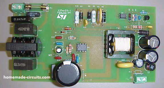
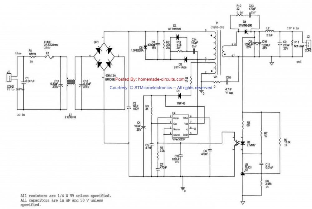
The circuit diagram of the proposed 12V 2 amp circuit using VIPer53-E could be witnessed in the below shown image:

DOWNLOAD COMPLETE PCB AND PARTS LIST
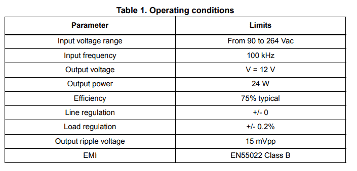
Main Operating Conditions can be studied through the following image:
Transformer Details:
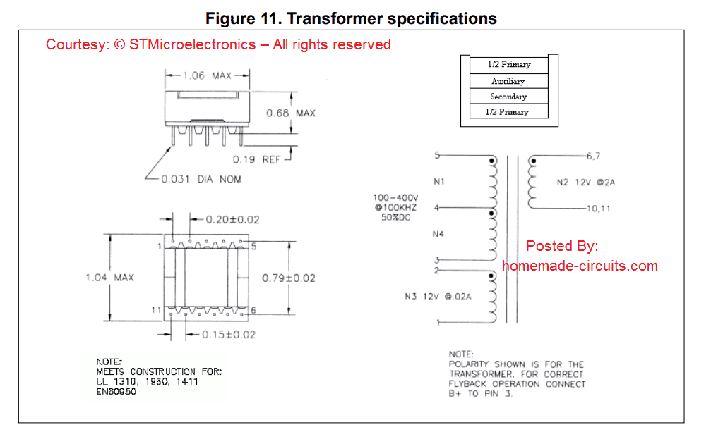
The ferrite core transformer winding details for the above SMPS circuit could be analyzed as per the data furnished in the following figure:
More Info on VIPer53-E can be studied in this article
Design#2: Introduction
The next design is based on the IC UC2842 from Texas Instruments, which can be also used for building a high grade, solid state, very reliable SMPS circuit rated at 12V, and with a current output @ 2 amp to 4 amps.
The complete circuit diagram of this design can be sen in the following figure:
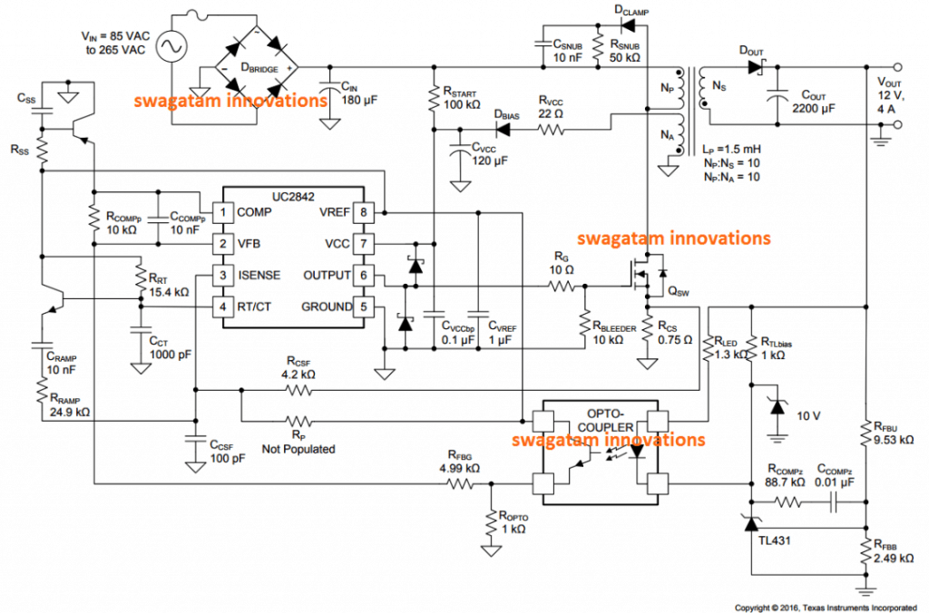
Let’s try to understand the functions and criticalities of a few of the main components used in this 12V 2 amp SMPS circuit:
Cin Input Bulk capacitor and minimum bulk voltage:
The shown bulk capacitor Cin may be incorporated using a single or a few capacitors in parallel, possibly by using an inductor across them to eliminate noise generated due to differential-mode conduction. The value of this capacitor decides the level of minimum bulk voltage.
If a lower value Cin is used to reduce minimum bulk voltage, might result in raised primary peak current overloading the switching mosfets and also the transformer.
On the contrary keeping the value larger might result in higher peak current on the mosfet and the trafo, which is also not acceptable, therefore a reasonable value as indicated in the diagram should be chosen.
It may be done by using the following formula:

Here Vin(min) indicate the RMS value of the minimum AC input voltage which is around 85 V RMS.
fLINE(min)denotes the frequency of the above RMS value which may be assumed to be 47Hz.
With reference to the above equation, in order to achieve a minimum of 75V bulk voltage value, at 85% efficiency, the Cin value will need to be around 126uF, in our prototype 180uF was found to be just fine.
Calculating the Tansformer turn ratios:
To begin with the transformer turn calculation, the most favorable switching frequency needs to be found out.
Although the IC UC2842 is specified to produce a maximum frequency of 500kHz, considering all the feasible and efficiency related parameters it was decided to select and set the device at around 110kHz.
This allowed the design to be reasonably well balanced in terms of the transformer size, EMI filter dimension and still keep the operations within the tolerable losses.
The term Nps refers to the primary of the transformer and this may be determined depending upon the rating of the driver mosfet used along with the rating of the secondary rectifier diode specifications.
For an optimal mosfet rating we first need to calculate the peak bulk voltage with reference to the maximum RMS voltage value which is 265V input AC in our case. Therefore we have:

For the sake of simplicity and cost effectiveness, a 650V rated mosfet IRFB9N65A was selected for this 12V 2 amp smps circuit prototype.
If we consider the maximum voltage stress on the mosfet drain to be around 80% of its specifications, and taking 30% as the permissible voltage spike from the maximum bulk input supply, the resultant reflected output voltage can be expected to be lower than 130V as expressed in the following equation:

Therefore for a 12V output the maximum primary/secondary transformer turn ratio or the NPS may be calculated as indicated in the following equation:

In our design a turn ratio of Nps = 10 has been incorporated.
This winding must calculated in such a way that it is able to produce a voltage that may be a little higher than the minimum Vcc specification of the IC, so that the IC is able to operate under optimal conditions and stability is maintained throughout the circuit.
The auxiliary winding Npa can be calculated as shown in the following formula:

The auxiliary winding in the transformer is used for biasing and providing the operating supply to the IC.
Now for the output diode, the voltage stress on it may be equivalent to the output voltage and the reflected input supply, as given below:

In order to counter the voltage spikes due to “ringing” phenomenon, a Schottky diode rated with a blocking voltage of 60V or higher was felt necessary and employed in this design.
Also to keep away high voltage current spike factor, this flyback converter is designed to work with a continuous conduction mode (CCM).
Calculating the Maximum Duty Cycle:
As discussed in the above paragraph, once we calculate the NPS of the transformer, the required maximum duty cycle Dmax can be calculated through the transfer function as allocated for CCM based converters, the details can eb witnessed below:

Transformer Inductance and Peak Current
In our discussed 12V 2 amp smps circuit the transformer magnetizing inductance Lp was determined as per the CCM parameters. In this example the inductance was chosen such that the converter is able to get into the CCM working zone with around 10% load and using minimum bulk voltage in order to keep the output ripple to the lowest.

For more details regarding the various technical specifications and formulas you can study the original datasheet here
Sir we are working on this same project.Can you share that which software you used for designing this circuit?
Abubakar, the circuits were taken from the datasheets of the IC.
hello sir!!
I’m sorry I don’t understand about SMPS hehehe
I want to ask, in the design#2,
what diodes are used in Dout, Dbias, Dclamp, in VCC and UC2842 output??
what transistors are used in npn and pnp??
what is the resistance at Rp and Rss??
and what is the capacitance on Css??
Thank you in advance sir
No problem Fernanady, I think to get a detailed information you should refer to the datasheet of the IC and the SMPS design
https://www.ti.com/lit/ds/symlink/uc3844.pdf
hello sir!!
I want to ask, in the design#2, what diodes are used in Dout, Dbias, in VCC and UC2842 output?? thank you in advance sir
Hi Fernandy, Dout can be any 5 amp schottky diode, Dbias can be any high speed rectifier diode such as FR107
Sir i need this 12V 2 Amp SMPS How to buy This ?
Mukesh, you can try searching “buy 12V 2 A SMPS” you should be able to find some useful online sources.
thanks sir, and also is the diode on the UC2842’s Output and VCC the same as Dout??
yes they are both schottky diodes
Hi dear
Thank you for your good information, I want to mass production 12v dc 2amp power supply for runnig CCTV. Could you please send me a circuit and datasheet with least component (a simple one but practical and safe)
Thank you so much for your help.
Sir please solve my problem Sir mere pass ek agriculture spray machine ka battery charger hai maine supply ko repairing ke time esme ek 5N60 power mosfet. Lgaa hai maine kaise ki kyaa lagaya aur series se check kiya turant hi mosfet dead ho jata hai please Sir kyaa problem ho sakte hai Sir Output side me ek LM358 IC bhi lgaa hai kyaa ic to dead nahi hai Sir
Guarav, without seeing the connections it can be impossible to judge the fault. If a MOSFET is connected wrongly it will burn instantly so you must know the pinout details before connecting it. The IC LM358 could be operating the MOSFET, so probably the IC may be fine….still without a practical check it may not be possible to advise a solution.
Hello Mr Swagatam. Pls I am having problems calculating the primary turns for my ferrite core transformer. I used this formula: Vin×10²/(4 ×freq.×Bmax×core area). The area of my core is 0.785cm², though I don’t have the datasheet of the transformer since it has no markings on it. My input Voltage is 23–33vdc. This is my test voltage because I intend using this transformer to build an SMPs running from the mains of 110–240VAC. I tried the transformer at a frequency of 146KHz, (flyback and forward topology). Using both of of these topologies at different times, my transformer would act as a short circuit once it’s drive circuit is powered on.
I don’t understand why this happens so, since I have followed the formula I found on this site, or is there another formula for the flyback transformer turns?
Hello Victory, the formula and the details presented in the following article is universally tested and is 100% correct. Please recheck your data and construction according to the details presented in the articles. It won’t be possible for me to verify your design without practically checking it.
https://www.homemade-circuits.com/how-to-design-and-calculate-ferrite-core-transformers-for-inverters/
Hello i want to design a 12v volt 10 amp adapter please help with the design
You can try to modify this design as per your specs.
https://www.homemade-circuits.com/smps-2-x-50v-350w-circuit-for-audio/
I can’t do this, please do، I need this circuit
Power supply 12v 10a
Sir, Please help me to make 12V, 2A SMPS . When power supply shutdown that time my Wi-Fi router working after power supply UP then battery automatically charging
Lipuna, you can try one of theses circuits
https://www.homemade-circuits.com/simple-dc-ups-circuit-for-modemrouter/
dear sir! what will be the possible value of the resistor and capacitor in soft start circuit of design#2, i mean Rss & Css also the pnp transistor used?
dear sheraz, you can set it up randomly, because it’s a simple RC time delay circuit. You can select C as 0.22uF and R as 100K, this might give you a good 0.5 or 1 second soft start delay. You can increase these values for higher soft start periods.
Hi sir,
I want to build 5V 2A SMPS… using your https://www.homemade-circuits.com/220v-smps-cell-phone-charger-circuit/ this circuit… please let me know if i can surely increase current to 2A by reducing secondary turns to 5turns.. and also can BA159 diode handle 2A at the ouput of ferrite transformer…?
please reply..Thanking in advance..
Hi Akshay,
I think it may be possible by decreasing the output or secondary turns to a proportional lower number, but BA159 will not handle anything more than 1amp if at all it is mounted on a heatsink.
what are modifications i need to do for that circuits then…FR107 diode can be used as replacement for BA159…what else…
you can use 3nos of BA159 or FR107 in parallel such that they are tightly assembled together and their bodies are pressed with each other, and their common leads are filled with a good amount of solder
ok thanks.. That part is fine but what about rest of the circuit…any more changes needed..?
for the secondary winding use bifilar enameled wire, meaning use many thin copper enameled wires in parallel while winding the turns, you can use 10 numbers of 30 SWG wires in parallel for the winding, no more changes may be required as far as I think
Thanks a lot Sir.. You are doing great job.. Best blog for learning…!!
It’s my pleasure Akshay, keep up the good work
hi.. can you suggest any other replacement optocoupler for SFH6106-1..?
Hi, you can search for “4 pin optocoupler”, any one from them will work… Just make sure the diagram shows an LED and transistor inside the package.
Sir,
This time I ask to you about a SMPS Transformer specification which is two tapping;
Primary voltage -325 volt Dc. 2A
Secondary voltage (1) -28.1v .15A
Secondary voltage (2)-16v. 15A .
Sir can you suggest a proper core for this switching transformer?
ETD44 is sufficient ?
please tell about the turns also.
Thanks
Ajitkumar
Ajit,
it can be difficult to estimate the size of the core, so I won’t be able to suggest much, as far as I know from practical experience, the core which will allow you to accommodate the winding perfectly without cramming or without leaving large amount of space will work the best. The winding accommodation within the cores should be just perfect…
Ok
Thanks
Hello Sir! Dear sir if we buy an already builtin switch mode transformer for specific rating, how will we can determine the primary, secondry and feedback winding of the transformer and the polarity(which winding is clockwise and anti clockwise) mean how to determine the start and end of each winding along with polarity?
Sheraz, that can be difficult, because we normally design the transformer as per the circuit specifications, doing the opposite can be risky and unpredictable. I am not sure about it…
It might require going through many formulas and calculations
sir i have remove 12v zener diode and add tl431 feedback block with pc817 but ouput voltage still does not regulate but continously fluctuate? will the output can be regulated to add both zener and tl431 feedback block. i have made the circuit just like the circuit you have posted in 220v smps cell phone charger tutorial, but wind the transformer for 12v , how to regulate output?
Hi Sheraz, I think I have already replied to your question yesterday…please refer to the previous answer
by the way which circuit diagram are you exactly referring to, please show me the link???
Hello sir! Dear sir i have design 12v power supply with TNY277 used 12v zener diode for output voltage regulation but the voltage continously change b/w 12v-35v mean does not show regulation, i have used bypass capacitor with C = 104pf and output filter capacitor C = 330uf what should i do to regulate the voltage fixed at 12v?
Sheraz, you will also have to adjust the Resistors RFbu RFbb correctly to keep the output stable.
Hi sir,
Could i use laptop 15v 3.5a charger for circuit includes: Nema 17,graphic tft lcd,arduino uno, arduino mega board, esp 8266 wifi, 11.1v 4400mah li ion battery,rehostate 5k, force sensor,relay 12v 10a.
Hi Shreyansh, you can use a 7812 IC in the middle for powering the Arduino boards and the relay circuit, another 7812 circuit for the W-Fi and for charging the 11.1 cell.
No it doesn't…
Does this ckt gives shock at output?
good day sir
which diode used in mosfet (flyback )
john
John, it is internally connected with the mosfet