In this post I will comprehensively explain regarding the fundamental working principles of semiconductor devices, and how the internal structure of semiconductors function under the influence of electricity.
The resistivity value between these semiconductor materials neither has a complete conductor characteristic nor a complete insulator, it is in between these two limits.
This feature may define the semiconductor property of the material, however it would be interesting to know how a semiconductor works between a conductor and an insulator.
Resistivity
According to Ohm's Law, the electrical resistance of an electronic device is defined as the ratio of the potential difference across the component to the current flowing through the component.
Now using resistance measurement can pose one problem, its value changes as the physical dimension of the resistive material changes.
For instance when a resistive material is increased in length, its resistance value also increases proportionately.
Similarly, when its thickness increased its resistance value decreases proportionately.
The need here is to define a material which may indicate a property of either a conduction or opposition to electrical current regardless of its size, shape or physical appearance.
The magnitude for expressing this particular resistance value is known as Resistivity, which has the synbol ρ, (Rho)
The unit of measurement for resistivity is Ohm-meter (Ω.m ), and it may be understood as a parameter which inverse of conductivity.
In order to get the comparisons between the resistivities of several materials, these are classified into 3 main categories: Conductors, Insulator, and Semi-conductors. The chart below provides the required details:

As you can see in the above figure, there’s a negligible difference across the resistivity of conductors like gold and silver whereas, there may be a significant amount of difference in the resistivity across insulators such as quartz and glass.
This is due to their response to ambient temperature which makes metals hugely efficient conductors than the insulators
Conductors
From the above chart we understand that conductors have the least amount of resistivity, which may be typically in microohms/meter.
Due to their low resistivity electrical current is able to pass through them easily, due to the availability of a large amount of electrons.
However these electrons can be pushed only when their is a pressure across the conductor, and this pressure can be formed a by applying a voltage across the conductor.
Thus, when a conductor is applied with a positive/negative potential difference, the free electrons of each atom of the conductor are forced to get dislodged from their parent atoms and they begin drifting across within the conductor, and is generally known as flow of current.
The degree at which these electrons are able to move depends on how easily they can be set free from their atoms, in response to a voltage difference.
Metals are generally considered good conductors of electricity, and among metals, gold, silver, copper, and aluminum are the best conductors orderly.
Since these conductors have very few electrons in the valence band of their atoms, they easily get dislodged by a potential difference and they begin jumping from one atom to the next atom through a process called "Domino Effect", resulting in a flow of current across the conductor.
Although gold and silver are the best conductors of electricity, copper and aluminum are preferred for making wires and cables due to their low cost and abundance, and also their physical sturdiness.
Despite of the fact that copper and aluminum are good conductors of electricity, they still have some resistance, because nothing can be 100% ideal.
Although small the resistance offered by these conductors can get significant with the application of higher currents. Eventually the resistance to higher current on these conductors is dissipated as heat.
Insulators
Contrary to conductors, insulator are bad conductors of electricity. These are generally in the form of non-metals and have very little vulnerable or free electrons with their parent atoms.
Meaning the electrons of these non metals are tightly bonded with their parent atoms, which are extremely difficult to dislodge with the application of voltage.
Due to this feature, when electric voltage is applied the electrons fail to move away from the atoms resulting in no flow of electrons and therefore no conduction takes place.
This property leads to very high resistance value to insulator, in the order of many million Ohms.
Materials like glass, marble, PVC, plastics, quartz, rubber, mica, bakelite are examples of good insulators.
Just like conductor, insulators equally play an important role in the filed of electronics. Without insulator it would be impossible to isolate voltage differences across circuit stages, leading to short circuits.
For example we see the use of porcelain and glass in high tension towers for transmitting AC power safely across the cables. In wires we use PVC for insulating positive, negative terminals, and in PCBs we use Bakelite in order to isolate copper tracks from each other.
Basics of Semiconductors
Materials like silicon (Si), germanium (Ge) and Gallium arsenide come under the basic semiconductor materials. It is because these materials have the characteristic of conducting electricity intermediately giving rise to neither proper conduction nor proper insulation. Due to this property these materials are named as semiconductors.
These materials exhibit very few free electrons across their atoms, which are tightly grouped in a crystalline lattice kind of formation. Still, the electrons are able to get dislodged and flow, but only when specific conditions are employed.
Having said this, it becomes possible to enhance the conduction rate in these semiconductor by introducing or substituting some kind of "donor" or "acceptor" atoms to the crystalline layout, enabling the release of extra "free electrons" and "holes" or vice versa.
This is implemented by introducing a certain amount of a external material to the existing material such as silicon or Germanium.
By itself, materials like silicon and Germanium are categorized as intrinsic semiconductors, due to their extreme pure chemical nature, and the presence of complete semiconductive material.
This also means that, by applying a controlled amount of impurity into them, we are able to determine the rate of conduction in these intrinsic materials.
We can introduce types of impurities referred to as donors or acceptors to these materials to enhance these with either free electrons or free holes.
In these processes when an impurity is added to an intrinsic material in the proportion of 1 impurity atom per 10 million semiconductor material atom, it is termed as Doping.
With the introduction of sufficient impurity, a semiconductor material could be transformed into an N-type or P-Type material.
Silicon is among the most popular semiconductor material, having 4 valence electrons across its outermost shell, and also surrounded by adjoining atoms forming a total orbits of 8 electrons.
The bonding between the two silicon atoms is developed in such a way, that it allows sharing of one electron with its adjoining atom, leading to a good stable bonding.
In its pure form a silicon crystal may have very few free valence electrons, attributing it the properties of a good insulator, having extreme resistance values.
Connecting a silicon material to a potential difference will not help any conduction through it, unless some kind of positive or negative polarities are created into it.
And to create such polarities, the process of Doping is implemented into these materials by adding impurities as discussed in the previous paragraphs.
Understanding Silicon Atom Structure
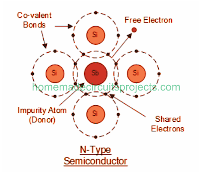
In the above images we see how the structure of a regular pure silicon crystal lattice looks like. For the impurity, normally materials like Arsenic, Antimony or Phosphorous are introduced within the semiconductor crystals turning them into extrinsic, meaning "having impurities".
The mentioned impurities are made up of 5 electrons on their outermost band known as "Pentavalent" impurity, for sharing with their adjoining atoms.
This ensures that 4 among the 5 atoms are able to join with the adjoining silicon atoms, excluding a single "free electron" which can be set free when an electrical voltage is connected.
In this process, because the impure atoms begin "donating" each electron across their nearby atom, "Pentavalent" atoms are named as "donors".
Using Antimony for Doping
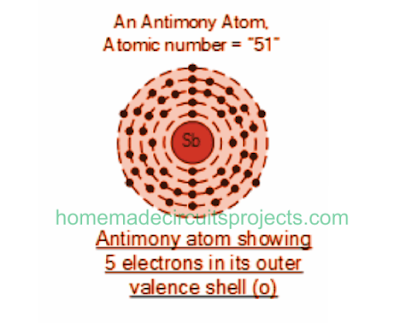
Antimony (Sb) and Phosphorous (P) often become the best choice for introducing "Pentavalent" impurity to silicon.

In Antimony 51 electrons are setup across 5 shells around its nucleus, while its outermost band consists of 5 electrons.
Due to this, the basic semiconductor material is able to acquire additional current carrying electrons, each attributed with a negative charge. Therefore it is named "N-type material".
Also, the electrons are named as "Majority Carriers" and the holes developing subsequently are termed as "Minority Carriers".
When an Antimony doped semiconductor is subjected to an electric potential, the electrons which happen to get knocked off are instantly substituted by the free electrons from Antimony atoms. However, since the process eventually keeps a free electron floating within the doped crystal, this causes it to be a negatively charged material.
In this case, a semiconductor may be termed a N-type if it has donor density higher than its acceptor density. Meaning when there are higher number of free electrons compared to the number of holes, causing a negative polarization, as indicated below.
Understanding P-Type Semiconductor
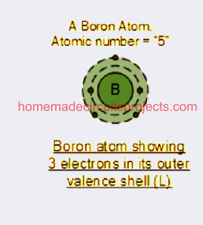
If we consider the situation conversely, introducing a 3 electron "Trivalent" impurity into a semiconductor crystal, for example if we introduce aluminum, boron, or indium, which contain 3 electrons in their valence bond, therefore a 4rth bond becomes impossible to form.
Because of this a thorough connection becomes difficult, allowing the semiconductor to have plenty of positively charged carriers. These carriers are called "holes" across the entire semiconductor lattice, due to a whole lot of missing electrons.
Now, due to the presence of holes in the silicon crystal, a nearby electron gets attracted to the hole, attempting to fill the slot. However, as soon as the electrons tries to do this, it vacates its position creating a new hole in its previous position.
This in turn attracts the next nearby electron, which again leaves a new hole while trying to occupy the next hole. The process goes on giving an impression that actually the holes are moving or streaming across the semiconductor, which we generally recognize as the conventional flow pattern of current.
As the "holes appear to move" gives rise to a shortage of electrons allowing the entire doped crystal to acquire a positive polarity.
Since each impurity atom become responsible for generating a hole, these trivalent impurities are called "Acceptors" due to the fact that these go on accepting free electrons continuously in the process.
Boron (B) is one of the trivalent additives which is popularly used for the above explained doping process.
When boron is used as a doping material, it causes the conduction to mainly have positively charged carriers.
This results in the creation of P-type material having positive holes called "Majority carriers", while the free electrons are called "Minority carriers".
This explains how a semiconductor base material turns into a P-type due to an increased density of its acceptor atoms compared to the donor atoms.
How Boron is used for Doping
Summarizing the Basics of Semiconductors
N-Type Semiconductor (Doped with a Pentavalent Impurity such as Antimony for example)
Such semiconductors which are doped with Pentavalent impurity atoms are termed as Donors, since they show conduction through the movement of electrons and therefore they are termed as N-Type Semiconductors.
In N-type Semiconductor we find:
- Positively charged Donors
- Abundant number of free electrons
- Relatively lesser number of "holes" compared to the "free electrons"
- As a result of doping, positively charged donors and negatively charged free electrons are created.
- The application of a potential difference results in the development of negatively charged electrons and positively charged holes.
P-Type Semiconductor (Doped with a Trivalent Impurity such as Boron for example)
Such semiconductors which are doped with Trivalent impurity atoms are termed as Acceptors, since they show conduction through the movement of holes and therefore they are termed as P-Type Semiconductors.
In N-type Semiconductor we find:
- Negatively charged Acceptors
- Abundant quantity of holes
- Relatively smaller number of free electrons compared to the presence of holes.
- Doping results in the creation of negatively charged acceptors, and positively charged holes.
- Application of a voltage filed causes the generation of positively charged holes and negatively charged free electrons.
By itself, P and N type semiconductors happen to be electrically neutral, naturally.
Commonly, Antimony (Sb) and Boron (B) are the two materials which are employed as doping members due to their abundant availability. These are also named as "mettaloids".
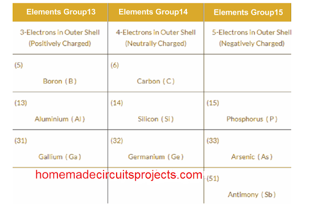
Having said this, if you look at the periodic table, you will find many other similar materials having 3 or 5 electrons in their outermost atomic band. Implies that, these materials can also become suitable for the doping purpose.
Periodic Table


Nice sir.
Sir can you suggest books to read about semiconductor basics.
Thank you
Thanks Y, presently I do not have a perfect tutorial on semiconductor devices but I will surely try to post one soon in this website.