In simple terms, biasing in BJTs may be defined as a process in which a BJT is activated or switched ON by applying a smaller magnitude of DC is across its base/emitter terminals so that its is able to conduct a relatively larger magnitude of DC across its collector emitter terminals.
The working of a Bipolar transistor or BJTs at DC levels is governed by several factors, that includes a range of operating points over the characteristics of the devices.
Under the section 4.2 I have explained in this article we will check the details regarding this range of operating points for BJT amplifiers. Once the specified DC supplies are calculated, a circuit design may be created for determining the required operating point.
A variety of such configurations are examined within this article. Every single model discussed will in addition identify the stability of the approach, meaning, exactly how sensitive the system could be to a given parameter.
Although numerous networks are examined within this section, they have one fundamental similarity between the assessments of each configuration, because of the following repeated use of the crucial fundamental relationship:

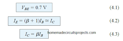
In the majority of situations the base current IB happens to be the very first quantity that needs to be established. Once IB is identified, the relationships of Eqs. (4.1) via (4.3) could be implemented to obtain the rest of the quantities in question.
The resemblances in evaluations are going to be quickly apparent as we advance with the subsequent sections.
The equations for IB are so very identical for many of the designs that one formula could be derived from the other one by simply removing or inserting an element or two.
The principal objective of this chapter is to establish a degree of understanding of the BJT transistor which would enable you to implement a DC analysis of just about any circuit having the BJT amplifier as an element.
4.2 OPERATING POINT
The word biasing showing up in the title of this article is an in-depth term which signifies implementation of DC voltages, and to determine a fixed level of current and voltage in BJTs.
For BJT amplifiers the resulting dc current and voltage create an operating point on the characteristics that establish the region which becomes ideal for the required amplification of the applied signal. Because the operating point happens to be a predetermined point upon the characteristics, it can also be referred to as quiescent point (abbreviated as Q-point).
"Quiescent" by definition signifies silence, stillness, sedentary. Figure 4.1 demonstrates a standard output characteristic of a BJT having 4 operating points. The biasing circuit could be developed to establish the BJT across one of these points or others inside the active region.
The maximum ratings are pointed out on the characteristics of Fig. 4.1 through a horizontal line for the highest collector current ICmax and a perpendicular line on the highest collector-to-emitter voltage VCEmax.
The maximum power limitation is identified from the curve PCmax in the same figure. On the bottom end of the graph we can see the cutoff region, identified by IB ≤ 0μ, and the saturation region, identified by VCE ≤ VCEsat.
The BJT unit could possibly be biased outside these indicated maximum limits, but the consequence of such process would result in being significant deterioration of the life of the device or total breakdown of the device.
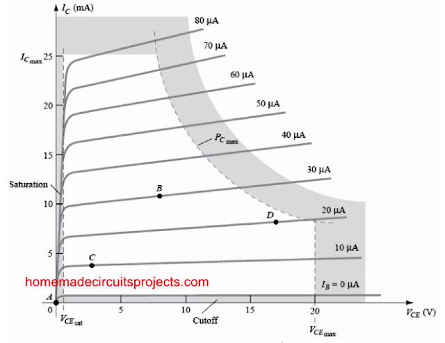
Restricting the values between the indicated active region, one may pick out a variety of operating areas or points. The selected Q-point usually is dependent on the intended specification of the circuit.
Yet, we can certainly take into account a few distinctions among the number of points illustrated in Fig. 4.1 to provide a few fundamental recommendations regarding the operating point, and therefore, the bias circuit.
If no bias were being applied, the device would at first remain entirely switched OFF, causing a Q-point to be at A - that is, zero current via the device (and 0V across it). Because it is essential to bias a BJT to enable it to react for the full range of a given input signal, point A may not look appropriate.
For point B, when a signal is connected to the circuit, the device will show a variation in current and voltage through the operating point, enabling the device to respond to (and perhaps amplify) both the positive and negative applications of the input signal.
When the input signal is optimally used, the voltage and current of the BJT will probably change..... however may be not sufficiently enough to activate the device into cut-off or saturation.
Point C might help certain positive and negative deviation of the output signal, but the peak-to-peak magnitude might be restricted to the proximity of VCE = 0V/IC = 0 mA.
Working at point C likewise may cause little worry with regards to the non-linearities due to the fact that the gap between IB curves could be altering quickly at this particular area.
Generally speaking, it is far better to operate the device in which the gain of the device is rather consistent (or linear), to guarantee that the amplification on the overall swing of input signal remains uniform.
Point B is a region exhibiting higher linear spacing and for that reason greater linear activity, as indicated in Fig. 4.1.
Point D establishes the device operating point close to the highest voltage and power levels. The output voltage swing at the positive limit is thus restricted when the maximum voltage is not supposed to be exceeded.
Point B as a result looks the perfect operating point with regards to linear gain and biggest possible voltage and current variations.
We will describe this in the ideally for small-signal amplifiers (Chapter 8) however, not always for power amplifiers, ....we'll talk about this later.
Within this discourse, I will be focusing mainly on biasing the transistor with regard to small-signal amplification function.
There's another extremely crucial biasing factor that needs to be looked at. Having determined and biased the BJT with an ideal operating point, the effects of temperature should also be evaluated.
Heat range will cause the device boundaries like the transistor current gain (ac) and the transistor leakage current (ICEO) to deviate. Increased temperature ranges will cause greater leakage currents in the BJT, and thus will modify the operating specification established by the biasing network.
This implies that the network pattern also needs to facilitate a level of temperature stability to ensure that temperature variations impacts are with minimal shifts in the operating point. This upkeep of the operating point could be stipulated with a stability factor, S, that signifies the level of deviations in operating point caused by a temperature change.
An optimally stabilized circuit is advisable, and the stable feature of several essential bias circuits will be evaluated here. For the BJT to be biased inside linear or effective operating region the below given points must be satisfied:
1. The base-emitter junction should be forward-biased (p-region voltage strongly positive), enabling forward-bias voltage of around 0.6 to 0.7 V.
2. The base-collector junction has to be reverse-biased (n-region strongly positive), with the reverse-bias voltage staying at some value inside the maximum limits of the BJT.
[ Remember that for forward bias the voltage across the p-n junction will be p-positive, and for reverse bias it is reversed having n-positive. This focus on the first letter should give you a way to easily remember the essential voltage polarity.]
Operation in the cut-off, saturation, and linear areas of the BJT characteristic are usually presented as I have explained below:
1. Linear-region operation:
Base-emitter junction forward biased
Base-collector junction reverse biased
2. Cutoff-region operation:
Base-emitter junction reverse biased
3. Saturation-region operation:
Base-emitter junction forward biased
Base-collector junction forward biased
4.3 FIXED-BIAS CIRCUIT
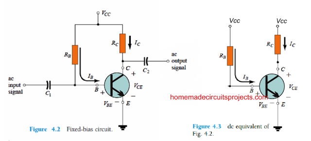
The fixed-bias circuit of Fig. 4.2 is designed with a fairly simple and uncomplicated overview of transistor dc bias analysis.
Although the network implements an NPN transistor, the formulas and calculations could work equally effectively with a PNP transistor setup simply by re-configuring the current flow paths and voltage polarities.
The current directions of Fig. 4.2 are the genuine current directions, and the voltages are identified by the universal double-subscript annotations.
For the dc analysis the design may be separated from the mentioned AC levels simply by swapping out the capacitors with an open circuit equivalent.
Moreover, the dc supply VCC could be split up into a couple of separate supplies (only for carrying out the evaluation) as proven in Fig. 4.3 just to allow a break up of input and output circuits.
What this does is minimizes the link between the two with the base current IB. The parting is unquestionably legitimate, as shown in Fig. 4.3 where VCC is hooked up straight to RB and RC just as in Fig. 4.2.
Forward Bias of Base–Emitter
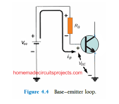
Let's first analyze the base-emitter circuit loop shown above in Fig. 4.4. If we implement Kirchhoff’s voltage equation in the clockwise direction for the loop, we derive the following equation:

We can see that the polarity of the voltage drop across RB as determined through the direction of the current IB. Solving the equation for the current IB provides us with the following result:

Equation (4.4)
Equation (4.4) is definitely an equation which can be easily memorized, simply by remembering that the base current here becomes the current passing through RB, and by applying Ohm’s law according to which current is equal to the voltage across RB divided by the resistance RB.
The voltage across RB is the applied voltage VCC at one end less the drop across the base-to-emitter junction (VBE).
Also, due to the fact that supply VCC and the base-emitter voltage VBE are fixed quantities, the choice of the resistor RB at the base establishes the amount of base current for the switching level.
Collector–Emitter Loop
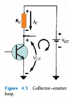

The figure 4.5 shows the collector emitter circuit stage, where the direction of the current IC and the corresponding polarity across RC have been presented.
The value of the collector current can be seen to be directly related to IB through the equation:
Equation (4.5)
You may find it interesting to see that since the base current is dependent on the quantities of RB, and IC is linked with IB through a constant β, the magnitude of IC isn't a function of the resistance RC.
Adjusting RC to some other value won't produce any effect on the level of IB or even IC, for so long as the active region of the BJT is maintained.
That said, you will find that the magnitude of VCE is determined by the RC level, and this may be a crucial thing to consider.
If we use Kirchhoff’s voltage law in the clockwise direction across the shown closed loop in fig 4.5, it produces the following two equations:

Equation (4.6)
This indicates that the voltage across the collector emitter of the BJT within a fixed bias circuit is the supply voltage equivalent to the drop formed across RC
To have a quick glance of single and double subscript notation recall that:
VCE = VC - VE --------(4.7)
where VCE indicates the voltage flowing from collector to emitter, VC and VE are the voltages passing from collector and emitter towards ground respectively. But here, since VE = 0 V, we have
VCE = VC --------(4.8)
Also because we have,
VBE = VB - VE --------(4.9)
and because VE = 0, we finally get:
VBE = VB --------(4.10)
Please remember the following points:
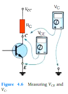
While measuring the voltage levels like VCE, make sure to put the red probe of the voltmeter on the collector pin and black probe on the emitter pin as shown in the following figure.
VC signifies the voltage passing from collector to ground and its measuring procedure is also as given in the following figure.
In the present case both the above readings will be similar, but for different circuit networks it could show varying results.
This implies that this difference in the readings between the two measurements could prove crucial while diagnosing a possible fault in a BJT network.
Solving a Practical BJT Biasing Example
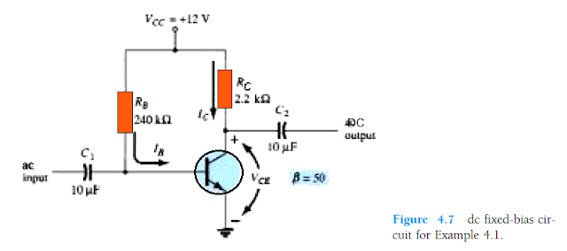
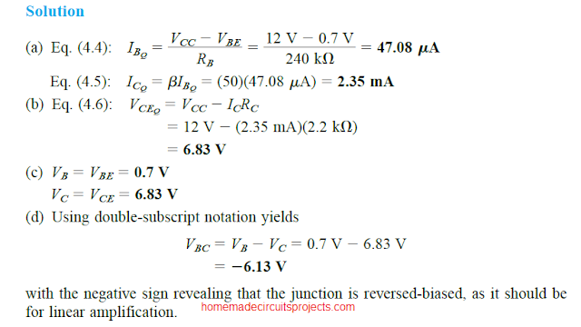
Evaluate the following for the fixed-bias configuration of Fig. 4.7.
Given:
(a) IBQ and ICQ.
(b) VCEQ.
(c) VB and VC.
(d) VBC.
In the next chapter I have explained about BJT Saturation.
Reference
hi swagatam, is it possible to conduct a dc analysis of a single stage bjt transistor rf amplifier with the collector consisting of an LC resonant circuit instead of a single resistor? My attempt is to find the reactance of the individual L and C then find the combine parallel reactance of them. there is also an RFC in series with the resonant circuit. I then add the series inductive reactance with the parallel reactance. i am not comfortable with the procedure and the answer. is this the proper method or is there a better way. thanks.
Hi Abdulalim, yes it may be possible, but can be a bit time consuming…