The DC to DC converter circuit described below can be used to convert a 24 V DC source into a 12 V DC output with high efficiency. Meaning, the circuit will allow to acquire a 12 V DC from a 24 V DC source with negligible power loss.
Being a switching regulator, this circuit is highly efficient and will not waste or dissipate energy, unlike linear regulators such as IC 7812, or IC LM317 or IC LM338.
Why Linear Regulators like 7812, LM317 and LM338 are Bad Step down Converters?
Linear regulators such as the 7812 and LM317 are considered inefficient step-down converters due to their operational characteristics.
In a linear regulator, the excess input voltage undergoes dissipation in the form of heat. This implies that the voltage drop between the input and output terminals is simply "burned off" as wasted energy. The linear regulator functions by acting as a variable resistor, adjusting its resistance to dissipate the surplus energy and regulate the output voltage.
This dissipation process leads to considerable power loss and low efficiency. The efficiency of a linear regulator is determined by the ratio of output power to input power.
As the input-output voltage difference increases, the power dissipated as heat, which is the voltage difference multiplied by the output current, also increases.
Consequently the efficiency diminishes as the voltage differential between input and output rises.
For instance, when using a linear regulator to regulate a 24 V input down to 12 V, the excess 12 V is dissipated as heat. This can result in substantial power wastage and necessitate additional cooling mechanisms in applications involving high power.
In contrast, switching regulators (such as buck converters) are more efficient for step-down conversion. They utilize a combination of inductors, capacitors, and switches to convert the voltage efficiently.
Switching regulators store energy during one phase of the switching cycle and deliver it during another, thereby minimizing the dissipation of energy as heat. Depending on the specific design, switching regulators can achieve efficiencies ranging from 80-95% or even higher.
In summary, while linear regulators like the 7812 and LM317 are straightforward and cost-effective, they are not the most efficient choice for step-down conversion when power efficiency is a significant concern.
Circuit Description
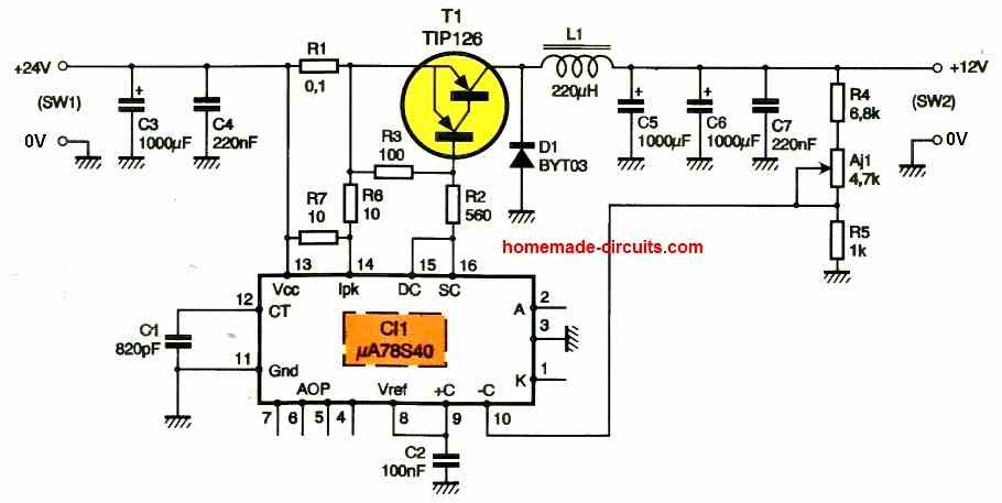
The figure below shows the basic diagram of the 24 V to 12 V converter.
The switching regulator used is a common model from Motorola: the µA78S40.
The following figure presents the internal structure of this integrated circuit, which includes various necessary components for a switching regulator: oscillator, flip-flop, comparator, voltage reference source, driver and switching transistors.
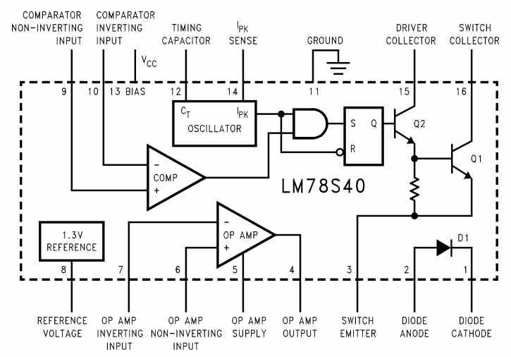
Additionally, there is an operational amplifier that is not needed for this application. Filtering and smoothing of the power supply are handled by capacitors C3 to C7.
Capacitor C1 determines the frequency of the oscillator, while resistors R1, R5, and R6 help limit the output current of the converter.
The voltage across resistor R1 is proportional to the current supplied by the converter.
By setting a voltage difference of about 0.3 V between pins 13 and 14 of the µA78S40, resistors R6 and R7 create a voltage divider, allowing current limitation to occur at around 5A.
The voltage reference source, decoupled by capacitor C2, is available at pin 8 of IC1.
This reference voltage is applied to the non-inverting input of the internal comparator of IC1. The inverting input is set to a potential proportional to the converter's output voltage.
To maintain a constant output voltage, the comparator controls the output stage of IC1.
Both inputs of the comparator are maintained at the same potential, and the output voltage is given by the following formula:
Vs = 1.25 * [1 + (R4 + Aj1) / R5].
The adjustable resistor Aj1 allows for adjusting the converter's output voltage in the range of +10V to +15V.
The two output transistors form a Darlington pair, and their successive switching is controlled by the flip-flop in sync with the oscillations of capacitor C1.
Combined with an AND gate, this flip-flop is controlled by the comparator to adjust the conduction time of the output stage of the µA78S40 and maintain a constant output voltage.
The saturated or blocked state of transistor T1 follows the state of IC1's Darlington pair. When IC1's output stage is saturated, transistor T1 is biased, and its base current is limited by resistor R2.
Resistor R3, together with resistor R9, forms a voltage divider, limiting the VBE voltage of transistor T1 at the beginning of the switching process.
Transistor T1, acting as a Darlington model, behaves as an open or closed switch at the frequency of the µA78S40's oscillator.
The inductor L1 allows for the voltage drop from 24V to 12V using the properties of inductance. In a steady state, when transistor T1 is saturated, a voltage of +12V is applied across inductor L1.
During this phase, the inductance stores energy, which it releases when the applied voltage disappears. Thus, when transistor T1 is blocked, inductor L1 tends to maintain the current flowing through it.
Diode D1 becomes conductive, and a counter-electromotive force of -12V appears across inductor L1.
Due to the conduction of diode D1, this counter-electromotive force is present across capacitors C5 and C6, ensuring their charge is maintained.
When the charge level drops below the comparator's threshold in IC1, transistor T1 enters conduction again.
This simplified explanation of the switching regulator's operation does not account for voltage drops caused by the forward voltage of diode D1 and the saturation voltage of transistor T1.
The residual output ripple of the converter depends, among other factors, on the capacitance.
Construction
The Figure below shows the layout of the tracks that will be reproduced using the method of your choice. The main power lines will have a wide width to accommodate high currents.
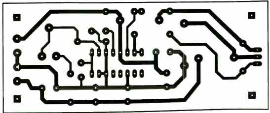
Once the circuit is printed and etched, these tracks can be tinned to enhance their conductivity.
The next Figure below shows the component placement.
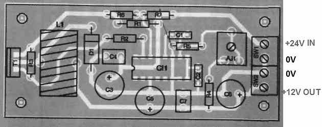
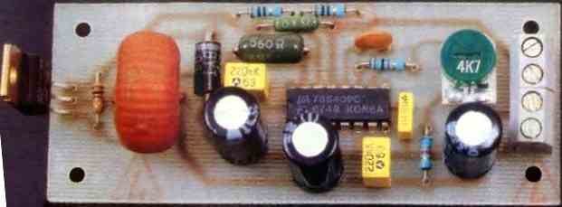
The inductor is a 5A toroidal model that can be made by winding enameled wire with a 1 mm cross-section on a high-flux toroid with an outer diameter of 21 mm and an inner diameter of 12.5 mm.
Using a toroidal inductor is preferred over a choke coil, like those used for triac noise suppression, because it provides better saturation flux density (more than twice as much).
The current-limiting resistor R1 is a miniature 0.1 Ohm model, which can be replaced by two 0.22 Ohm / 1W resistors soldered in parallel.
Special attention should be given to capacitor C3, as the 24V voltage may be exceeded in a running vehicle due to its alternator/regulator system designed to maintain battery charge.
Therefore, the voltage rating of this capacitor should be at least 35V. The heat sink should be selected with a thermal resistance of less than 3°C/W to ensure its temperature remains within a suitable range during continuous operation.
For example, with an ambient temperature of 18°C, a reference heat sink like the SEEM CO220P, 10cm long and mounted vertically, would reach a temperature of around 50°C with a continuous load current of 3 A.
You can also find this heat sink referenced as SL204, and the ML25 is a similar heat sink model, but other models with suitable thermal resistance can be considered.
Additionally, the ML41 reference heat sink is of very good quality, and a 5cm long version is sufficient.
The switching transistor T1 should be insulated from the heat sink using a mica insulator and an insulating sleeve.
Applying silicone grease will improve thermal dissipation. Apply a thin layer of silicone grease to both sides of the mica insulator.
For testing purposes, 12 V automotive bulbs can be used as a load, and the output voltage can be adjusted using the adjustable resistor Aj1. Finally, the assembly will be installed in a metal housing.
The final built prototype image.
Reference : LM78S40 Datasheet
Using LM63635 IC
In the following content I have explained how to build an adjustable switching step down regulator for converting a 24V DC input into a 12V DC output, using the IC LM63635.
About LM63635
The LM63635-Q1 is an innovative synchronous peak-current-mode buck regulator, meticulously engineered to cater to a broad spectrum of automotive applications.
This versatile regulator seamlessly transitions between pulse frequency modulation (PFM) and pulse width modulation (PWM) based on the load's specific requirements.
Under heavy loads, it adeptly operates in PWM mode, maintaining a consistent switching frequency.
Conversely, when the load becomes lighter, the regulator gracefully shifts to PFM mode with diode emulation, facilitating discontinuous conduction mode (DCM).
This intelligent transition reduces the input supply current and effectively preserves efficiency.
The key features of this device encompass a range of functionalities:
- Customizable switching frequency to suit your application's demands.
- The ability to activate Forced PWM mode (FPWM) when necessary.
- Frequency synchronization for enhanced precision.
- Flexibility to choose the desired output voltage as per your requirements.
Setting the Output Voltage
The LM63635D-Q1 determines its output voltage based on the input condition of VSEL. In a scenario, when a fixed 5-V output is needed, VSEL can be directly linked to VCC, and the FB input is directly connected to the output capacitor.
However, in cases where an adjustable output voltage is desired, using the LM63635C-Q1 version, an external feedback divider becomes necessary. As depicted in the following circuit diagram, this divider network consists of RFBT and RFBB, which closes the feedback loop between the output voltage and the converter.
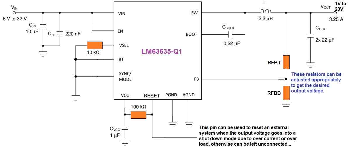
In this situation, a 10-kΩ resistor is connected from the VSEL input to the ground. The converter ensures the output voltage's regulation by maintaining the voltage on the FB pin at the same level as the internal reference voltage, which is 1-V.
The resistance of the divider is a trade-off between preventing excessive noise interference and avoiding excessive load on the output.
Smaller resistance values reduce sensitivity to noise but also decrease efficiency at light loads. The recommended value for RFBT is 100 kΩ, with 1 MΩ being the maximum allowable value.
If 1 MΩ is chosen for RFBT, it is essential to incorporate a feedforward capacitor across this resistor to ensure sufficient loop phase margin.
Once RFBT is determined, The following formula is used to select the appropriate value for RFBB, with VREF typically set at 1 V.
RFBB = RFBT / [(VOUT/VREF - 1)]
The above formula can be solved to set the feedback potential divider network appropriately, for getting a 12V DC output from a 24V DC input source.
Reference: LM63635D-Q1 Datasheet
Hi Swagatham,
I am an electronics enthusiast and a design engineer on power and analog. I really feel so happy to see your work. I really appreciate your contribution to this fraternity. I wanted to do something similar, but could not do it due to work load. Feels so happy that someone like you have created an excellent knowledge base… Hats off to you… Love you.
Thank you so much Bipin, for your encouraging words, I appreciate it very much.
Please feel free to discuss and share any circuit-related questions that you may have…I’ll be most happy to answer!
Can the 24V-12V 30A Converters be stacked to give 60A?
Yes, that may be possible.
Sir, I want 3 ampere o/p current then what can I do in this cct?
OK, for 3 amp current you can replace the existing transistor with TIP147 transistor and make sure the inductor wire is thick enough to handle 3 amps current..
Thanks sir, what is o/p current of this cct?
Hi M.Ahsan, current will be around 1 amp.
Hey! Sir what is the main purpose of using inductor in this circuit ?
Hello Ahsan, the inductor is used to control the output voltage, through a current controlled pwm switching of the inductor….
Hey Mr. Swagatam it’s me again with a couple of questions about this DC/DC conv… First, is what value for inductance would you suggest to work in a circuit that needs to handle 50 to 70amps? Of course then I would need to know wire gauge and inductor core to use for that piece. I’m wanting to go with the 2.2kufd/amp but that’s a LOT of capcacitance. So I’m thinking a lot less would be sufficient. The other is this, I haven’t really studied the circuit yet but it looks like this basic IC driver would be fine to drive a darlington which would need to fire some MOSFETs. Then which MOSFETs would you use if you were to build such a circuit? I have some 75A @ 80v P channels I was thinking would be suitable. The plan is for building my off grid solar running my RV to a point I would reconfig from 12v to 24v and then use a dropper circuit to run the 12v circuits already in place. I have a 60A MPPT on the way that will work all the way up to a 48v input which would never run any higher than 24v out but it is capable of running up to 6 units in parallel using RS485 sync system and a WiFi/etc. with another combiner system. As I mentioned long ago, I’m not an EE just a hobby builder that went to school a long time ago, forgotten so much of my electronics training since then. It comes down to whether I can build this for a reasonble project or just purchase a unit from Victron or some other brand. The MPPT is just to much to take on, and get one that truly works. I’m still working on simpler controller to keep my auto batteries charged while sitting idol. 1’s working for now and I’m working a couple others and some different schematic designs to see how they work and which does a better job.
Hey Bret,
Sorry, I do not have the necessary formulas to calculate the wire thickness and the core spec of the inductor. I think these can be best done by some trial and error. A 3 mm thick wire should be enough I think for 70 amp current. Also the IC cannot be changed since the since the IC pinouts are specifically configured with the buck converter circuit with feedback which cannot be perhaps replicated perfectly. However I have a similar circuit which can be also tried, using a TL494 IC.
https://www.homemade-circuits.com/5v-pwm-solar-battery-charger-circuit/