A compact, battery-powered transmitter emits a LASER beam when the control push button is activated. The beam is frequency-coded to provide a maximum level of reliability in transmission. The receiver can be located at a considerable distance from the transmitter (up to several tens of meters).
The light beam, by definition, remains highly focused, and the diameter of the circular spot observed at a distance of 10 meters is significantly less than a centimeter.
The transmission can be direct or indirect, using interposed angled mirrors depending on the topography of the area.
The receiver primarily consists of an LDR (Light Dependent Resistor) cell, amplification, signal frequency control, and specific utilization.
In this article, we will review three examples of receiver circuits:
- A Laser entry doorbell
- A Laser timer
- A Laser Delay relay switch
Laser Transmitter Driver Circuit
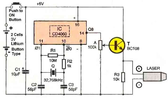
The energy source required for powering the circuit is provided by two 3V lithium batteries, which together form a 6V power supply that is activated by pressing the push-button switch BP.
Given the low power consumption of the circuit (a few mA), the battery life is very long: thousands of activations.
Capacitor C1 regulates the power level, considering the pulsed nature of the LASER transmitter operation. The integrated circuit IC is a CD4060. It is a 14-stage binary counter with a time base driven by a 32,768 kHz quartz crystal for obvious reasons of frequency stability.
Thus, at the Q8 output, a square wave signal is obtained with a frequency characterized by the value: F = f0 / 28 = 32768 / 256 = 128 Hz.
The transistor T is connected as a voltage follower. By adjusting the adjustable resistor A, it is possible to extract a more or less significant fraction of the delivered square wave amplitude from the Q8 output of IC.
It is necessary to adjust the resistor so that at the emitter of the transistor, the square waves have a maximum value corresponding to the minimum power supply potential of the mini LASER transmitter that has been obtained.
There are transmitters that operate at a nominal voltage of 3V or 4.5V.
We will discuss the practical details of adjusting this resistor at the end of the article.
Doorbell Receiver
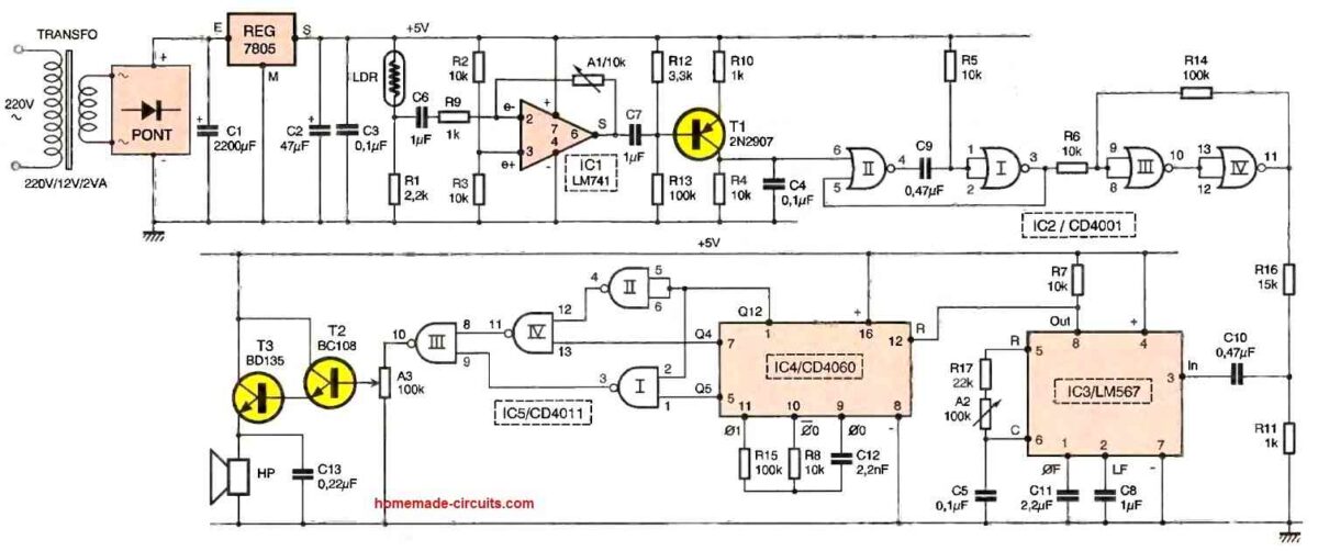
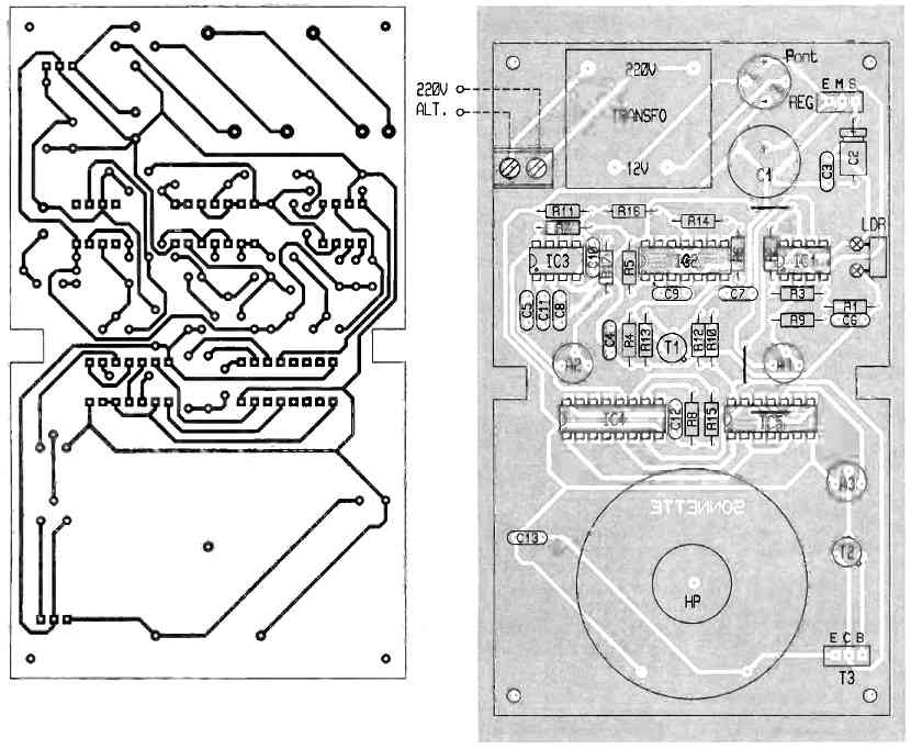
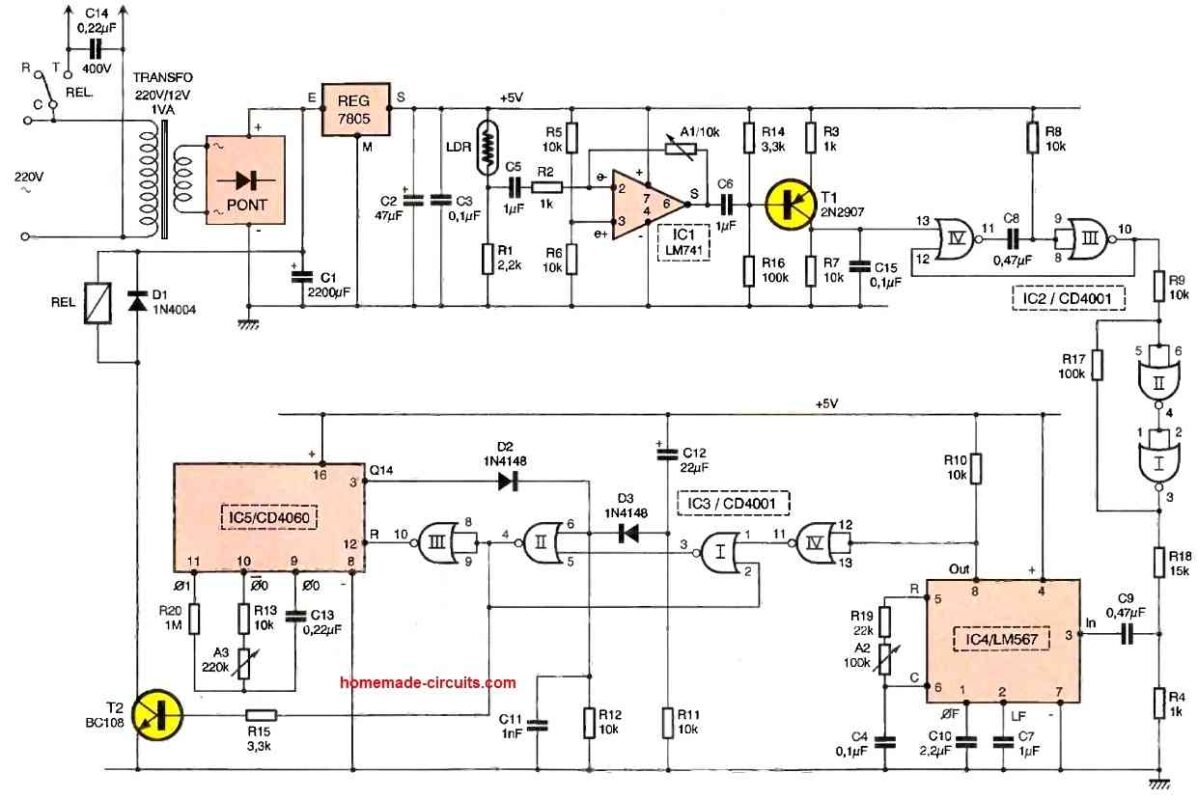
The energy required for the operation of the receiver is drawn from the 220V distribution mains through a power transformer, which provides an AC potential of 12V at its secondary winding.
A diode bridge rectifies both half-cycles, while capacitor C1 performs initial filtering. A regulated 5V DC potential is obtained at the output of a 7805 regulator.
This value is determined by the presence of a specific integrated circuit, the LM567, which will be discussed later.
Capacitor C2 provides additional filtering, while C3 decouples the power supply of the actual circuit.
Signal Reception
The LASER beam strikes the active surface of an LDR, which is a photoresistor.
It should be noted that such a component reacts to visible light (including LASER) by exhibiting an ohmic resistance that decreases as the incident light intensity increases.
The integrated circuit IC1 is a very common "741" configured as a preamplification stage.
The signals from the junction point of LDR/R1 are directed to the inverting input via C6 and R9.
By adjusting the slider of adjustable resistor A1, it is possible to control the gain of this amplification stage.
The higher the ohmic resistance of the adjustable resistor used for feedback, the higher the gain value increases.
In the idle state, a potential of 2.5V is observed at the output of the 741, a value determined by the voltage divider R9/R3 connected to the non-inverting input.
Signal Shaping
The PNP transistor T1 is configured as a common emitter amplifier. Its base is biased in such a way that in the absence of signals, the collector of T1 maintains a zero potential.
However, when LASER signals are received by the LDR, positive pulses are collected at the collector of T1, which are then directed to the input of the monostable flip-flop formed by NOR gates I and II of IC2.
This flip-flop outputs a series of high states with a duration of 3.3 ms.
Since the signals have a frequency of 128 Hz, corresponding to a period of 7.8 ms, the generated signal closely resembles a square wave configuration.
NOR gates III and IV of IC2, along with the peripheral resistors R6 and R14, form a Schmitt trigger.
It delivers square wave signals at its output with well-defined rising and falling edges.
Lastly, the combination of R1 and R forms a voltage divider.
The output of this voltage divider produces square wave signals with an amplitude of approximately 310 mV, a value set for proper operation of the downstream integrated circuit IC3.
Frequency Detection
The IC3 circuit is an LM567. It is an active filter.
We won't go into the details of how this component operates.
Towards the end of the article, we provide additional information about this highly sophisticated integrated circuit.
For now, let's simply understand that if the frequency of the signal fed into the "IN" input via C10 is recognized as correct, the "OUT" output, which is normally driven high by R7, switches to a low state.
It remains in this state as long as the analyzed signal's frequency is deemed acceptable by IC3.
The adjustment of this tuning frequency is done through the slider of adjustable resistor A9. We will discuss this further later on.
Ring Signals
The IC4 circuit is a CD4060. In standby mode, with its "RESET" input held high, the counter is locked. All the Qi outputs are in a low state.
As soon as the "RESET" input is brought low, the integrated circuit becomes operational.
In particular, on pin Q0 (9), a square wave with a period of approximately 48 μs is observed, corresponding to a frequency of around 20.8 kHz.
On the Q4 output, the observable signal frequency is calculated as 20800 / 24 = 1300 Hz, and on Q5, it becomes 650 Hz.
These are two musical frequencies separated by an octave.
At the Q12 output, the delivered square wave signal has a frequency of 20800 / 212 = 5 Hz.
This means that a sequence of high states followed by low states is observed, with each state lasting 100 ms.
Therefore, NAND gates I and IV are alternately active, producing square wave signals of 650 Hz for gate I and 1300 Hz for gate IV. An unutilized gate maintains a high output state.
At the output of NAND gate III, a musical signal is obtained that changes frequency every 0.1 s, giving it a characteristic modulation resembling a telephone ringtone.
Amplification
The NPN transistors T2 and T3 form a Darlington pair.
As a reminder, such a configuration, acting as a voltage follower, provides significant current gain.
The current intended for powering the moving assembly of the speaker's diaphragm is collected at the input of T3.
The speaker then reproduces the sound of the signal mentioned above. By adjusting the slider of adjustable resistor A3, it is possible to achieve a higher or lower sound intensity.
Receiver for Timer (Power supply, signal reception, and processing)
These sub-components are identical to those explained in the previous chapter regarding the doorbell.
Timer Arming
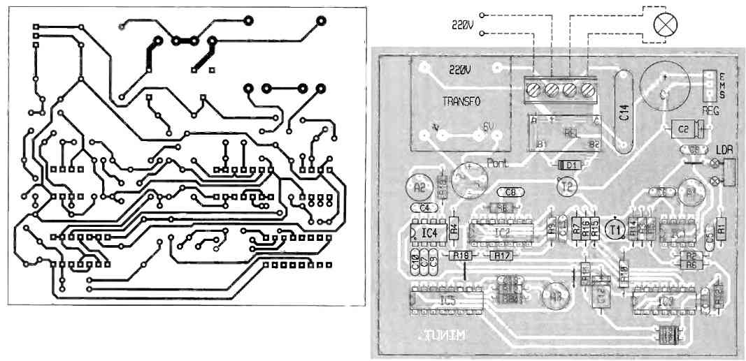
When the LM567 IC4 recognizes the conformity of the signal present at its input, the output of NOR gate IV in IC3 goes high.
NOR gates I and II in IC3 form an R/S (Reset/Set) latch.
Such a latch maintains a stable high output state on its output (gate II) once its input 1 in gate I has been momentarily set to a high state.
It returns to the stable low resting state if its input 6 is briefly set to a high state.
Relay Operation
Once the R/S latch output goes high, transistor T2 enters saturation.
In its collector circuit, it includes a coil of a 12V/1RT relay. It's important to note that the relay is directly powered by the 12V potential available at the positive terminal of C1.
The relay closes, directly supplying power to the pilot lighting circuit through the timer.
Diode D1 protects transistor T2 from the effects of self-induced voltage spikes that occur mainly during relay openings.
End of Timer
The IC5 circuit is a CD4060. In the standby state, with its RESET input held permanently high, the oscillator section is blocked, and all the Qi outputs are in a low state.
However, as soon as the RESET input is brought low due to the activation of the R/S latch, the counter starts.
Specifically, at pin 9, a square waveform is observed, and its period is adjustable using the slider of adjustable resistor A3. If "t0" represents the value of this period, the value that characterizes the Q14 output is determined by the relation T = 2^14 × t0.
More precisely, the exact moment when a rising edge is observed on Q14 corresponds to half a period of the signal present on this pin. This means that the rising edge occurs after a duration of ΔT = 2^13 × t0.
Depending on the angular position of the slider of adjustable resistor A3, the timing can be set from 1 to 15 minutes.
As soon as a rising edge occurs on the Q14 output, via diode D29, the R/S latch returns to its resting position. As a result:
- The utilization relay opens.
- The ICs counter is reset.
- The counter is blocked.
Receiver for Time Delay Switch
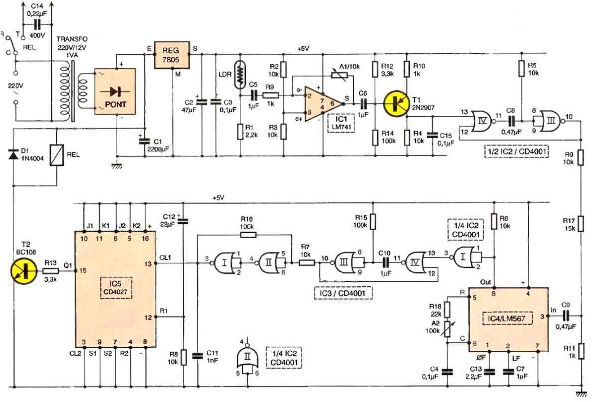
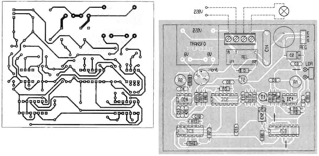
Control of the bistable flip-flop
Once IC4 recognizes the valid LASER signal, the output of NOR gate I in IC2 goes high.
The monostable flip-flop formed by NOR gates III and IV in IC3 becomes operational.
Specifically, it delivers a high state output for a duration determined by the values of R15 and C10. In the present case, this duration is approximately 70 ms.
The Schmitt trigger formed by NOR gates I and II in the same integrated circuit ensures that the signal has well-defined rising and falling edges.
Bistable flip-flop
The integrated circuit IC5 contains two bistable flip-flops, but only one of them is utilized in this circuit.
Each rising edge on the "CLOCK1" input causes a change in the state of the output Q1.
When the circuit is powered on, the capacitor C12 charges through R8.
This results in the automatic initialization of the flip-flop, causing its output Q1 to be set to a low state consistently.
How to use
The output Q1 supplies power to the base of the NPN transistor T2 through R13. This transistor controls the load relay under the same conditions as described in the previous circuit.
Construction
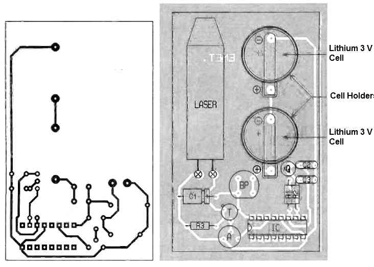
Their construction does not require any particular remarks.
As usual, all reproduction methods can be used: direct application of transfer elements on the epoxy copper, creation of a template, or photographic method.
After etching the circuits in a ferric chloride bath, the modules should be thoroughly rinsed with warm water.
Then, all the pads should be drilled with a 0.8 mm diameter drill bit. Some holes may need to be enlarged to 1 or even 1.3 mm in diameter to accommodate larger component connections.
Component Layout (Figure 7)
After placing the jumpers, diodes, resistors, and integrated circuit sockets should be positioned.
Then, solder the capacitors, transistors, and trimmers, and finally, proceed with the thicker components.
Pay careful attention to the orientation of polarized components.
Any mistake at this stage not only jeopardizes the operation of the circuit but can also lead to the destruction of certain components.
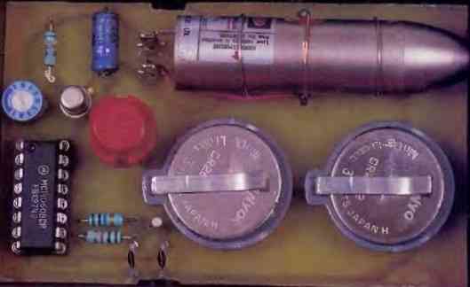
The LASER emitter should be directly glued to the epoxy to secure it mechanically. The same applies to the speaker.
Fine-tuning (Transmitter Module)
The goal is to adjust the trimmer potentiometer (A) to supply the LASER emitter with its maximum voltage.
Start by initially setting the potentiometer to its minimum position in the counterclockwise direction.
This ensures that the potential delivered by the emitter of transistor T is zero.
Next, remove the integrated circuit from its socket and connect pins 14 and 16.
Using a meter and rotating the potentiometer in the clockwise direction, adjust the potential available at the emitter of transistor T to the required nominal value specified by the LASER.
Module "Doorbell"
The trimmer potentiometer A1 is used to adjust the gain of the amplifier stage. Usually, the middle position of the potentiometer is suitable.
Turning the potentiometer clockwise increases the gain.
As for the trimmer potentiometer A2, it is used to tune the detection frequency of the LM567.
Starting from the middle position, explore the areas to the left and right of this position by making slow and slight rotations of the potentiometer.
The goal is to achieve a clear and stable low state on pin 8 when the LASER beam is directed at the LDR.
Finally, the trimmer potentiometer A3 adjusts the power of the sound output. It increases when the potentiometer is turned clockwise.
Module "Timer"
The trimmer potentiometers A1 and A2 are adjusted in the same way as in the previous circuit.
As for the trimmer potentiometer A3, it is used to set the duration of the timer.
The duration increases when the potentiometer is turned clockwise.
It is worth noting that the timer can be set from 1 to 15 minutes.
To increase the duration, you can replace the capacitor C13 with a larger value, such as 0.47 μF. In this case, the obtained timings will double in duration.
Module "Time-delay switch"
Only the trimmer potentiometers A1 and A2 are adjusted following the same principles as mentioned in the previous circuits.
Hello, I am a machine manufacturer. There is a laser receiver that I use in the machine. This receiver must be able to see 360 degrees and 25mm up and 25mm down. We do level control with this. Our laser gives 635nm 10khz square wave light. We are having problems in our receiver part, can you help us with this?
Can you please explain, what problem exactly you are facing with your receiver unit?
Our problem is that it works incorrectly and confuses when nearby.
How do you want it to work, please provide some technical speculations.
Swag, I have fabricated a grading box using a gate operated by a 12VDC linear actuator controlled by a laser receiver with machine control. I use two SPDT ice cube style relays which work perfectly in manual but when in automatic mode, the relays flutter quite a bit. I thought converting to solid state relays might do the trick but i can’t find any rated to 25 amps.
Hi Dan,
A solid-state relay might not be required. You can prevent the relays from chattering by doing the following things:
If the two SPDT relay are wired to work together, you can replace them with a single DPDT relay.
Connect a 220uF/25V capacitors right across the relay coil.
Let me know if these suggestions help you to solve the problem.
Swag,
If I use DPDT, I couldn’t figure out how it would work if it is on grade(not calling for either up or down movement-neutral, no movement) I appreciate the help. If you have an address, I can send a schematic of way I have going. Thx again
Yes, a schematic would help, because I having difficulty understanding the statement….”on grade(not calling for either up or down movement-neutral, no movement)
You can send it to:
homemadecircuits
@gmail.com
Thank you Dan,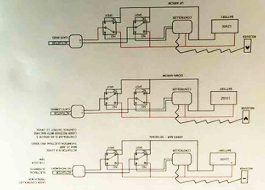
I saw the schematic which you sent me in my email ID.
I have downloaded it in the following link:
" rel="ugc">
From the schematic it is clear that the two SPDT relays are not operating simultaneously, rather are independent of each other.
Therefore they cannot be replaced with a DPDT relay.
In that case, you can simply try adding separate, individual capacitors across the two relay coils, in order to prevent the relay chattering.
The value of the capacitor can be anything between 100uF/25V and 470uF/25V.
Make sure to connect the capacitors with correct polarity, across the relay coils.
Let me know if that helps!
Swag,
I swapped out the ice cube relays with automotive type thinking they might be more durable but I am now experiencing some fluttering again. I can switch back or perhaps changing the capacitors might work. Currently in use is 100 uF/25. Would 470 uF be better or maybe 16vdc?
Update: I tried 470uF/25 and it rendered the control unit inoperative so it will have to be an alternative solution. Thank you
Thanks Dan, for the updates.
That’s strange? A capacitor across the coil terminals of a relay may cause a slight delay in its operation, but it can never render the relay or the control input inoperative.
Did you connect the capacitor with right polarity, because a reversed polarity can cause the source supply to short circuit?
Looking at the diagram you sent, the upper terminals of the relays appear to be connected to the positive supply, while the lower coils terminals connected with the switching source.
" rel="ugc">
The diagram is not very clear so I am finding it difficult to understand the details.
Can you send a clearer image of the same?