The popular 3 terminal fixed regulators available today are in the form of IC 7805, IC 7809, IC 7812, IC 7815, and IC 7824, which correspond to fixed voltage outputs of 5 V, 9 V, 12 V, 15V, and 24 V.
These are called fixed voltage regulators since these ICs are able to produce excellent stabilized fixed DC output voltages in response to a much higher unregulated DC input voltage.
These high end monolithic voltage regulators can be very cheaply purchased nowadays, which is normally less costlier and less complicated to work with, compared to building discrete regulator circuit equivalents.
These 3-terminal regulators are incredibly easy to wire, as can be viewed in the circuit diagram below that demonstrates the standard method by which these ICs are implemented.
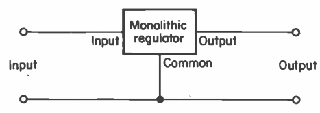
The three terminals of the IC are for apparent reasons, designated with the names input, common and output.
The supply positive and negative are simply connected across the input and common terminals of the IC respectively, while the regulated stabilized voltage is acquired across the output and common terminals.
The only discrete external part optionally demanded are a capacitor on the input and the output leads of the IC. These capacitors are necessary to enhance the level of output regulation of the device, and to improve the transient response. The microfarads values of these capacitors are generally not critical, and therefore are normally anything between 100 nf, 220 nf or 330 nf.
Types of 78XX Series Regulators
The most popular and widely used types of fixed voltage, monolithic voltage regulators are the 78XX series positive regulators, and the 79XX series negative regulators.
These are found with 3 output current specifications. They provide you with 9 positive types and nine 9 negative types of variants, as revealed in the chart below.
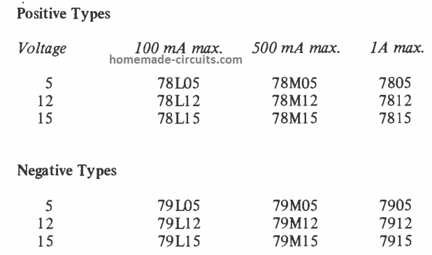
These 78XX series of ICs come with additional voltage ratings both in positive and negative forms. Standard ranges for these 78XX regulators are 8 V, 9 V, 10 V, 18 V, 20 V and 24 V, which correspond to ICs 7808, 7809, 7810, 7818, 7820, 7824 ICs.
Many of these devices carry suffix characters or figures with their printed number, depending on the manufacturer or the brand type.
However, all of them are essentially the same with identical rating. Several part dealres will not actually promote these ICs by type number, rather just point out their polarity, voltage and current specs, and occasionally with reference to their package style.
Main Features
These ICs feature in-built current limiting and short circuit protection for the output load. In medium and high power 78XX series of regulators this feature is generally of the foldback type. Foldback current limiting is a condition in which an output overload is simply not responded by the output current due to an automatic current limiting.
What is Foldback Current Limit
The foldback reaction of a foldback current limiting circuit can be witnessed in the following figure, that distinctly demonstrates how the output current minimizes under overload conditions to typically less than 50 % the ideal output current. The primary reason for employing foldback current limiting is that it significantly cuts down the dissipation within the regulator under short circuit situations.
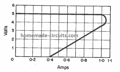
The foldback current limiting response can be understood from the following explanation:
Suppose we have 7805 IC with a 10 V input and it undergoes a short circuit across its output terminals. In this situation under ordinary type of current limiting the output of the IC will continue to generate 1 amp current giving a dissipation of 10 watts. But with a special foldback current limiting the short circuit current may get restricted to around 400 mA, resulting in a dissipation in the device of only 4 watts only.
Thermal Shutdown Feature
The majority of monolithic voltage regulators likewise also feature an in-built thermal shutdown protection circuitry. This feature helps to reduce the output current in the event the device goes through an overheat situation.
These types of voltage regulator ICs are as a result extremely robust, and never easily damaged even when these are incorrectly use. That said, one way through which they could be destroyed is by application of a high input supply voltage than the specified range.
You will find variations in the maximum tolerable input voltages specified by different suppliers for these ICs of the identical standard type, although 25 volts is apparently the minimum offered range for any 5 volt device (7805). Greater voltage regulators can handle a minimum of 30 volts, while for 20 and 24 volt varieties the input range is up to 40 volts.
For the circuit to work correctly the input voltage must be higher by 2.5 volts than the required output voltage, with the exception for 7805 regulator where the input voltage is supposed to be just more than 2 V above the required 5 V output, meaning it should be minimum 7 V.
Standby Current without Load
The quiescent current or the idle current consumption of these ICs without any load at the output can be between between 1 and 5 mA, although this may be up to 10 mA in some very high power variants.
Line and Load Regulation
The line regulation for all 78XX regulator ICs is smaller than 1%. Meaning, the output voltage may show a variation of less than 1% regardless of the input voltage variation from the maximum and minimum input voltage range.
The load regulation is also normally lower than 1% for most of these devices. This features ensures that the output will continue to provide the rated constant output voltage irrespective of the output loading conditions.
The ripple rejection feature for most of these regulator ICs is in the vicinity of 60 dB along with an output noise level which may be lower than 100 microvolts.
Power Dissipation
When you use these 78XX regulator ICs you must remember that these ICs are rated to handle only a finite amount of power dissipation. Hence, under highest output load the input voltage should never be allowed to exceed a few volts higher than the maximum tolerable input limit.
The maximum power dissipation at normal room temperature (25 degrees Celsius) for the low, medium, and high power 78XX ranges of devices is 0.7 watts, 1 watt and and 2 watts respectively.
The above limitation could be significantly improved to 1.7 watts, 5 watts and 15 watts respectively if the devices are mounted on a substantially big heatsink. The power dissipated in all these regulator devices is proportionate to the difference between the input and output voltages, multiplied by the output current.
How to Apply Heatsink to 78XX ICs
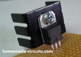
In this situation when the device is fully loaded at around 800 mA, the dissipation from the device could be as much as 4 watts (0.8A x 5V = 4W).
This appears to be two times more than maximum permisible 2 watts PD for the 7815 device. This implies that the extra 2 watts has to be compensated through a heatsink.
A broad selection of heatsinks are generally available in the market, and these are identified with rating of a particular degrees/watt.
This rating basically indicates the temperature rise that is caused for every single watt of power dissipated via the heatsink. This also indicates that for larger heatsink, the degrees per watt will proportionately lower.
The lowest size of heatsinking necessary for a 78xx regulator device could determined in the following way.
We have to primarily find out the nominal atmospheric temperature where the device is being used. Except if the device is likely to be used in an uncommonly warm surroundings, a figure of around 30 degrees Centigrade can be considered a reasonable assumption.
Safe Temperature Rating
Next, it may be essential to learn the maximum safe temperature rating for the specific 78XX regulator IC. For monolithic 78XX regulators this range may be at 125 degrees Centigrade. Having said that, this is actually the junction temperature, and not the case temperature which the IC can withstand.
The absolute maximum permissible case temperature is around 100 degrees Centigrade. Therefore it becomes important not to allow the device temperature to increase above 70 degrees Centigrade (100 - 30 = 70).
Because a power of 2 watts may result in a rise in temperature of a maximum of 70 degrees, a heatsink rated to dissipate of 35 degrees Centigrade/watt or less (70 degrees divided by 2 watts = 35 degrees C per watt) will be good enough.
Practically, a relatively bigger heatsink should be employed, since the heat transfer is never very efficient in most cases.
Furthermore, to get a long lasting stability it must be ensured that the device is ideally operated at somewhat below the rated maximum permissible temperature range.
If at all possible ensure a reasonable margin +/- 20 degrees or maybe more.
When the regulator IC is enclosed inside a container and covered away from the free atmosphere, may cause the trapped air in the container to warm up by the regulator dissipation. This might in turn cause the other sensitive parts on the PCB to to work under warmer conditions. Such situation might call for a larger heatsink for the regulator IC.
Application Circuits
A typical application circuit of a power supply using a fixed voltage 78XX monolithic voltage regulator can be seen below.
In this design a 7815 IC is used as the regulator IC which provides us with around +15 volts at approximately 800 mA current.
The transformer used is rated with 18 -0 - 18V for the secondary with a current rating of 1 amp.
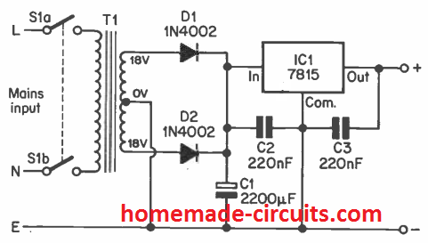
It is connected to a push-pull full wave rectifier which provides an unloaded voltage of about 27 V Dc after being filtered through C1.
Capacitors C2 and C3 work like input and output decoupling capacitors which should be attached relatively closer to the body of the IC. When the output load is full you will see the applied input voltage to the IC1 attaining a level at 19 to 20 volts, allowing approximately 5 volts difference across the input/output of the regulator.
How to Make Dual Power Supply Circuit
Since fixed voltage 78XX monolithic regulators can be purchased both in negative and positive variants, they appear perfect for implementing dual balanced power supplies.
When, for instance, a regulated supply is needed for operating an op amp based circuit with positive and negative supplies of 12 volts at 100 mA, the design shown in the following figure could be applied.
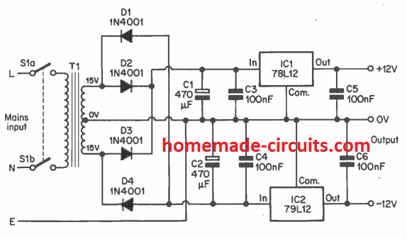
In this example, T1 is a 15-0-15 volt transformer rated with secondary current rating of 200 mA or more. You can find a couple of push-pull full wave rectifiers; D2 and D3 that give you a positive output.
D1 along with D4 deliver a negative output. The positive supply is filtered by C1 while the negative line is cleaned and filtered by C2.
IC1 gives you a regulated positive supply output, while the IC2 works like a negative supply regulator. C3 to C6 are positioned like decoupling capacitors for enhancing the output efficiency in terms of better response to spikes, noise and transients.
Higher Output Voltage using series Regulator Circuit
The configuration shown above could also be utilized for getting combined voltage values of the two regulators. Meaning , if the 79L12 is replaced with 78L12 regulator will enable the output to be 24V.
In such configuration, the 0V line may be ignored, and the +24V output may accessed directly across the positive and negative lines of the output.
Higher Output Voltage using Series Diode Circuit
It is actually very easy to get a small voltage boost at the output utilizing some rectifier diode between the ground pin of the IC and the ground line.
This approach enables the user to access a little higher voltage level which may not be directly obtained from any ready made regulator device.
The exact technique of wiring this configuration can be witenessed in the following image.
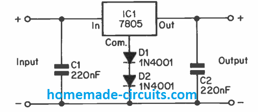
In this example we have estimated the required output voltage to be approximately 6V, and have implemented the same through a 5 volt regulator IC by boosting the output by 1 volt.
As can be seen, this 1 V elevation is effectively achieved by simply incorporating a couple of series rectifiers diodes with the common lead of the regulator.
The rectifiers are wired to make sure they are forward biased through the quiescent current utilized by the regulator, and which moves via the common GND terminal of the device.
The attached diodes as a result behave somewhat like low voltage zener diodes, wherein each diodes drops around 0.5 to 0.6 volts enabling a combined zener voltage of about 1 to 1.2 volts.
The objective of the design is to lift the common terminal of the regulator by 1 volt over the ground supply potential. Here the regulator 7805 IC actually stabilizes the rated output at 5 V above the ground line, hence, by elevating the ground terminal by around 1 V, the output is also lifted by the very same magnitude, causing the output also to get regulated at approximately 6 V level. This procedure works extremely well with all three terminal 78XX voltage regulator ICs.
Biasing Resistor for the Diodes
However in some cases you may have to attach an external resistor across the GND and the output pin of the IC to aid some extra bit of current to diodes, so that they are able conduct optimally for the intended results.
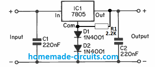
Since each rectifier diode will facilitate a forward drop of around 0.65 V approximately, by calculating more such diodes in series we can achieve proportionately higher level of boosted voltage across the IC output.
However, for this to happen the input level must be higher by at least 3V than the final estimated output level. Silicon diodes like 1N4148 will work quite nicely for the application.
Alternatively if diodes look cumbersome, a single equivalent zener diode could be also used for getting the same effect, as shown in the following example.
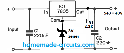
Having said that, please make sure that the procedure is implemented for getting not more than 3 V higher than the actual rating of the device. Beyond this level the output stabilization may get affected.
Increasing Current Capacity
Another great modification to a 78XX regulator could be implemented for achieving an increased output current higher than the maximum rating of the device.
One method of doing this is shown below.
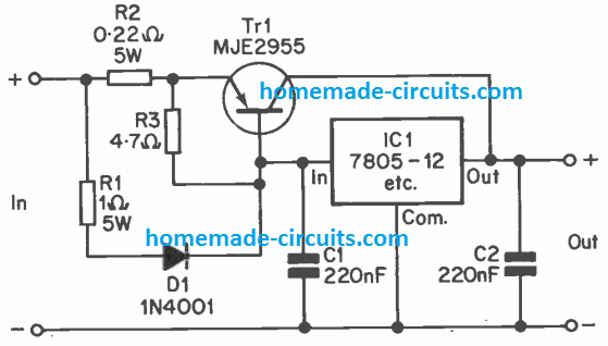
The indicated R1, and R2 configuration ratio assures that for every milliamp current that passes through R1, D1 and the regulator, a bit of current in excess of 4 mA is shifted via Tr1 and R2.
As a result when the full 1 amp is used through IC1, we have a current of more than 4 amps passing via Tr1. This situation allows the circuit to deliver a optimum output current which is a bit higher than 5 amps.
Even in an overload conditions, the currents through Tr1 and IC1 continue to have a ratio of somewhat higher than 4 :1, therefore, the current limiting feature of the IC continues to work without issues.
Circuits of this form have actually proved to be needless nowadays because of the availability of higher power regulators devices like the 78H05, 781-112 etc that come with a maximum current rating of 5 amps, and enable the user to configure them exactly with the same ease as the lower current counterparts.
I’m replacing a 78L05 soic8 on a circuit board. I can see signs of burn-out residue emanating from connector 5 and the datasheet lists connectors 4 & 5 as “nc”. I’m hoping nc stands for “not connected” in this instance. If nc were to meant “normally closed” it wouldn’t make much sense to me.
Problem is I cant find any trace of a contact shoe under connector 5 and I’m wondering if that contact shoe could have been destroyed in the burn-out event. Connector 4 which is also “nc” has a contact shoe.
Q. What does nc stand for?
nc may stand for normally closed, or not connected.
Thanks for the opinion. I went ahead with no contact to connector 5 on the 78L05 and the the unit now seems to be functioning as it should. It is located on the output circuit of a battery management board for a metal detector so $300 saved. NC must mean Not Connected in this instance.
OK great, thanks for updating the information.
Hi Swagatam! Is it possible to take the output from a 7809 and feed it to the input of a 7805 to spread the heat dissipation between the two regulators?
Hi Norman, yes that’s possible, the heat would be dissipated depending upon the input/output differential for the two ICs
I’m using a 7815 and 7915 for a split power supply for some TL072 op amps that are part of an audio pre-amp and also a Baxandall tone circuit. The data sheet for the 7815 has a few different sample application circuits. One is called a “fixed-output regulator” and uses only a couple of caps for the power pins as usual. Another sample circuit is called a “split-power supply” and shows a 7815 and 7915 used together, along with some diodes and extras caps, to form dual output dc power supply for an op amp.
My question is, is there an advantage to using the split-power supply design over using a separate 7815 and 7819 in a fixed-output regulator setup to create the positive and negative power rails for the op amps? The split-power supply design uses more parts, but I’m already using a 7815 and a 7819 in the fixed-output regulator set up to provide power to my op amps and it seems to be working fine.
Thanks for your help!!
Using 7815 and 7915 looks more suitable, although any other similar alternative will also work. However, using 7815 and 7819 might produce asymmetrical outputs, so they don’t seem to be the correct options. If the outputs are similar then the devices can be used without any issues, so both ICs should be identical either 7815 or 7819, and powered from separate transformers.
Thank you!
Hi
tnx for your tips and guides. they were helpful. would mind designing the current boost circuit with NPN like 2n3055 + 7805?
Hi Thanks, I will try to design it if possible, however you can also try the 1st design shown in the following article:
https://www.homemade-circuits.com/12v-car-laptop-charger-circuit-using/
sorry i want a +5v supply with capacity 2 A output.
You can try the last circuit in the above article, but with pnp