The following article which discusses a 300 watt pure sine wave inverter circuit with automatic output voltage correction, is a modified version of one of my previous posts, and was submitted to me by Mr. Marcelin. I have explained more about the converter implementations.
The Design
The idea was inspired by the design presented in this article by me, however Mr.Marcelin has refined it considerably for better efficiency and reliability.
To me, the modifications and the implementations done look great and feasible.
So I have explained the design elaborately with the following points:
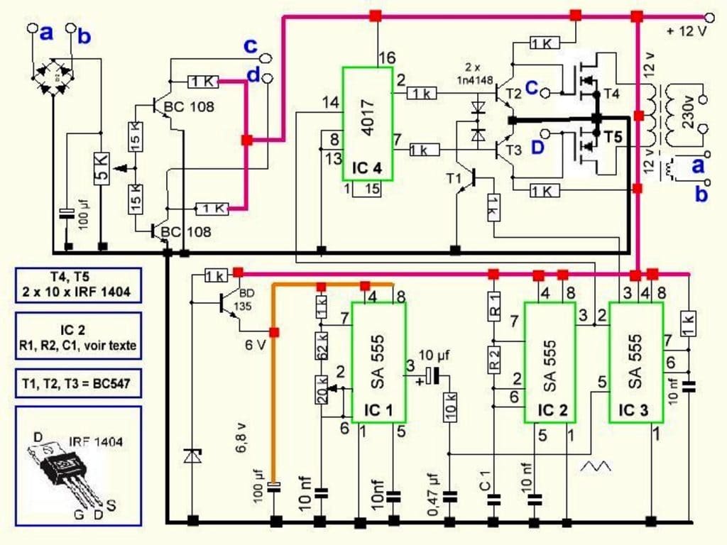
IC2 and IC3 are specifically configured as the PWM generator stage.
IC2 forms the high frequency generator required for pulsing the PWM waveform which is processed by IC3.
For processing the IC2 pulses, IC3 needs to be fed with a sine wave equivalent information at its pin#5, or the control input.
Since creating sine waveform is a bit complex than a triangular waves, the later was preferred as its easier to make yet performs as good as a sine waveform counterpart.
IC1 is wired up as the triangular wave generator, whose output is finally fed to pin#5 of IC3 for the generating the required RMS sine equivalent at its pin#3.
However the above processed PWM signals needs to be modulated over a push-pull kind of arrangement so that the waveforms are able to load the transformer with alternately conducting current.
This is necessary for achieving an output mains consisting of both positive and the negative half cycles.
Circuit Operation
The IC 4017 is introduced just for implementing this action.
The IC generates a sequentially running output from its pin#2 to pin#4, to pin #7, to pin#3 and back again to pin#2, in response to every rising pulse edge at pin #14.
This pulse is derived from the output of IC2, which is set to 200 Hz strictly so that the outputs of IC4017 results in a 50 Hz across the sequencing from the above discussed pin outs.
Pin#4 and pin#3 are purposely skipped, for generating a dead time across the gates triggers of the respective transistors/mosfets connected to the relevant outputs of IC4017.
This dead time makes sure that the devices never conduct together even for a nano second at transition zones, and thus safeguard the health of the devices.
The sequencing positive outputs at pin#2 and 7 trigger the respective devices which in turn force the transformer to saturate with the alternating battery power induced in the respective winding.
This results in the generation of around 330+ V AC at the output of the transformer.
However this voltage would be a square wave with high RMS if it wouldn't be processed with the PWM from IC3.
Transistor T1 along with its collector diode is fed with the PWM pulses such that T1 now conducts and grounds the base trigger voltages of the outputs devices in accordance with the PWM content.
This results in an output that's an exact replica of the the fed PWM optimized input..... creating a perfectly carved pure sine wave AC equivalent.
The circuit has additional features such as a manual output voltage correction circuit.
The two BC108 transistors are stationed for controlling the gate drive voltage levels of the mosfets, the base current of these transistors are derived from a small sensing winding on the transformer which provides the required output voltage level information to the transistors.
If the output voltage goes beyond the expected safe level, the base current of the above transistors may be adjusted and reduced by varying the 5K preset, this in turn brings down the conduction of the mosfets, ultimately correcting the output AC to the required limits.
The BD135 transistor along with its base zener provides a stabilized voltage to the associated electronics for sustaining constant PWM output from the relevant ICs.
With IRF1404 as the mosfets, the inverter would be able to generate anywher around 300 to 5000 watts of pure sine wave output.

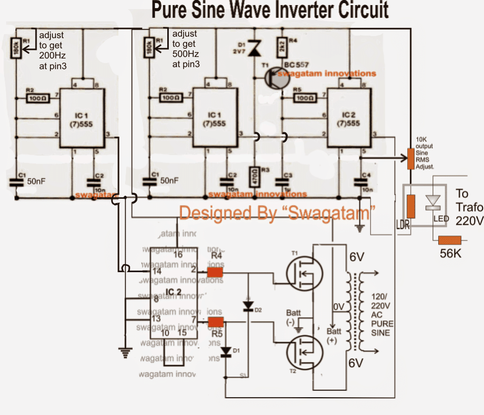
Many drawbacks and flaws were detected while assessing the above circuit details. The finalized circuit (hopefully) is presented below.
The above circuit may be further enhanced with an automatic load correction feature as shown below. It is implemented by the inclusion of the LED/LDR opto-coupler stage.

For the final verified design of the above circuit please refer to the following post:https://www.homemade-circuits.com/2013/10/modified-sine-wave-inverter-circuit.html
