Audio amplifiers which are designed to amplify an analogue audio signal through pulse width modulation or PWM processing and with adjustable duty cycle is known by many names including digital amplifier, Class-D amplifier, switched amplifier and PWM amplifier. (Article Contributed by: Ritu khanna)
Because it can perform at high efficiencies, a Class-D amplifier has become a favorite concept for mobile and public address applications where distortion is negligible.
Why PWM Amplifiers are so Efficient
It is because they convert the analogue audio signal into equivalent PWM modulated content. This modulated PWM audio signal is efficiently amplified by the output devices such as MOSFETs or BJTs and then converted back into high power analogue version using special inductors across the connected loudspeakers.
We know that semiconductor devices such as MOSFETs, and BJTs "do not like" to be operated in undefined regions of an input signal and tend to become hot. For example a MOSFET will not properly turn on when the gate signals is below 8V, and BJTs will not respond correctly at below 0.5 V base drive, resulting in high amount of heat dissipation through their body heatsink.
Analogue signals being exponential by nature force the above devices to work with uncomfortable and unfavorable slow rise and slow fall potentials, causing high heat dissipation and greater inefficiencies.
PWM amplification concept in contrast, allow these devices to work by either switching them fully ON or switching them OFF fully, without intermediate undefined potentials. Due to this, the devices do not radiate any heat and the audio amplification is rendered with high efficiency and minimum losses.
Advantages of Digital Amplifier Compared to Linear Amplifier
- Digital or PWM amplifiers use PWM processing and therefore the output devices amplify the signals with minimum heat dissipation. Linear amplifiers use emitter follower design and dissipate high amount of heat during sound amplification.
- Digital amplifiers can work with less number of output power devices compared to linear amplifiers.
- Due to minimal heat dissipation, no heatsink or smaller heatsinks are required, compared to linear amps which depend on large heatsinks.
- Digital PWM amplifiers are cheaper, lighter, and highly efficient compared to linear amplifiers.
- Digital amps can operate with smaller power supply inputs than linear amplifiers.
In this post, the first PWM power amplifier below is operated by a 6 V battery and generates up to 5W output power. Given its blatant output capacity, the PWM amplifier is often found in megaphones.
A common issue with mobile AF amplifiers is that due to their low-efficiency property it is difficult to produce high power from a low supply voltage.
However, the PWM amplifier in our discussion has almost 100% efficiency at a distortion level that is acceptable with megaphones and related P.A. devices. A few factors that contribute to the design are I have explained below:
Pulse-width modulation
The principle of Pulse Width Modulation (PWM) is represented in the below Figure 1.

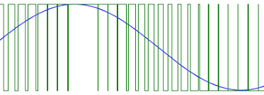
The concept is simple: the duty cycle of a rectangular signal of higher frequency is controlled by an input signal. The switch-on time of the pulse is relative to the instantaneous amplitude of the input signal.
The amount of the on-time and off-time in addition to the frequency is constant. Therefore, when an input signal is missing, a symmetrical square wave signal is produced.
To achieve relatively good sound quality, the frequency of the rectangular signal must be double than the highest frequency in the input signal.
The resulting signal may be used to power a loudspeaker. Figure 4 shows a clear conversion in the oscilloscope trace.
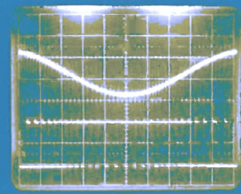
The upper trace shows the output signal post-filtering and measured across the loudspeaker. The amplitude of the remaining PWM signal that is overlapping the sine wave is small.
Electronic Switches as Amplifiers
Figure 2 describes the standard operation of the PWM amplifier with help of the block diagram.
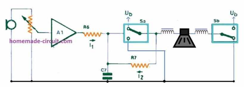
Let’s assume when the input is short-circuited, switch Sa powers capacitor C7 with a current I2. This ensues until a suitable upper limit switching voltage is achieved.
Then, it connects R7 to ground. After that, C7 is discharged to the lower limit switching voltage of Sa. As a result, C7 and R7 produces a square wave with a frequency of 50 kHz.
When an AF signal is effected to the input of the amplifier, the additional current I1 relatively reduces or increases the charge time, or increases and decreases the discharge time.
So, the input signal modifies the duty factor of the square wave signal which is seen at the output of the loudspeaker.
There are two laws which are essential for the basic operation of the PWM amplifier.
- The first is switch Sb is controlled in anti-phase with Sa while holding the other loudspeaker terminal as an alternative voltage to that of the PWM signal.
This setup produces an outcome of the switching bridge-type power output stage. Afterwards, at each polarity, the loudspeaker is forced with the full supply voltage so that a maximum current consumption is achieved.
2. Secondly, we look into inductors L1 and L2. The purpose of the inductors is to integrate the rectangular signal and convert them into sinusoidal as shown in the scope trace earlier. Furthermore, they also function and harmonics suppressor of the 50 kHz rectangular signal.
High Sound Output from a Modest Design
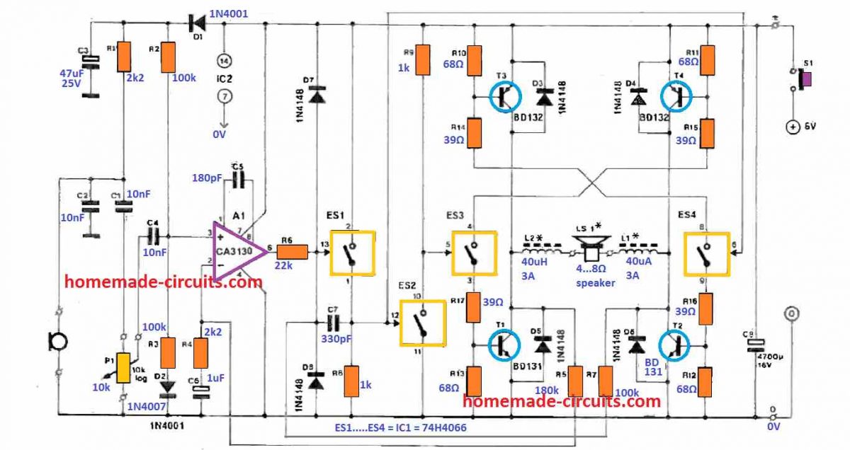
From the schematic in the above figure, you can easily identify the electronic components used in the block diagram.
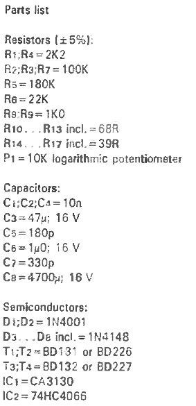
A handful of parts like resistor R1, coupling capacitors C1 and C4, volume control P1 and an amplifier based around opamp A1 does the biasing job for a capacitor (or electrostatic) microphone.
This whole operation creates the input segment of the PWM amplifier. As discussed earlier, switches Sa and Sb are built by electronic switches ES1 to ES4 and transistor pairs T1-T3 and T2-T4.
The part indications for the electronic components that construct the PWM generator relate to those described in the block diagram.
Probably the PWM amplifier is uncommonly efficient because the output transistors are not heated up even when forced with an all-drive condition. In short, there is practically zero dissipation in the power output stage.
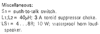
The most vital factor you need to consider before selecting inductors L1 and L2 is that they must be able to channel 3 A without becoming saturated.
The actual inductance consideration comes only second. For example, the inductors used in this project were obtained from a light dimmer.
The purpose of diodes D3 to D6 is to contain the back EMF produced by the inductors to a reasonably safe value.
Moreover, the non-inverting input of opamp A1 is formed by D1, C3, D2 and R3. This input voltage, efficiently filtered, is equal to half the supply voltage.
When using a traditional opamp amplifier, the voltage gain is assigned by a negative feedback loop. R4 and R5 will set the gain to 83 to make sure sufficient microphone sensitivity.
In case you’re using high impedance signal sources, R4 can be amplified as needed.
L1 and L2 cause the phase shift and because of that, feedback is possible with the assistance of the square wave signal at the collector of T1 compared to the sinusoidal loudspeaker signal.
Combined with C5 the opamp delivers the significant integration of the PWM feedback signal.
The feedback system lessens the amplifier’s distortion but not so extensively that you might use it for other application besides the public address.
Normally, a significantly increased amount of supply voltage and a complicated circuit design would be required for a Class-D amplifier with low distortion.
Implementing this setup would hamper the overall efficiency of the circuit. Pay attention when choosing electronic switches in the amplifier as HCMOS types are suitable ones.
A typical CMOS Type 4066 is extremely sluggish and inappropriate to trigger a “short-circuit” across T1-T3 and T2-T4. Not only that, but there is also a heightened risk of overworking or even permanently damaging the amplifier.
PWM Amplifier for Megaphone Application
Electronic enthusiasts prefer to employ the class-D amplifier for powering a horn-type loudspeaker because it can produce the loudest sound for a selected power level.

Using a 6 V battery pack and a pressure chamber loudspeaker, the amplifier model was easily constructed.
The existing 4 W of output power was measurable in a megaphone with decent audio range.
Four 1.5 V dry batteries or alkaline monocells were connected in series to supply voltage for the megaphone. In case you want to use this setup frequently, opt for a rechargeable NiCd or gel-type (Dryfit) battery.
Since the maximum current consumption of the megaphone is 0.7 A, a standard alkaline is suitable to support the operation for 24 hours at full output power.
If you plan for non-continuous use, choosing a set of dry cells will be more than enough.
Bear in mind that whatever power source you use, it must never cross more than 7 V.
The reason is the HCMOS switches in IC1 would not function properly at that voltage level or more.
Luckily, for the amplifier, the maximum threshold for supply voltage is larger than 11 V.
Another Good PWM Amplifier
A well designed PWM amplifier will comprise a symmetrical rectangular wave generator.
The duty cycle of this rectangular wave is modulated by the audio signal.
Rather than operating linearly, the output transistors operate as switches, so they are either completely on or off. In a dormant state, the duty cycle of the waveform is 50%.
That means every output transistor is fully saturated or also known as conducting, for the same duration. As a result, the average output voltage is zero.
This means if one of the switches stays closed a little longer than the other, the average output voltage will either be negative or positive depending on the input signal’s polarity.
Therefore, we can observe that the average output voltage is relational to the input signal. This is because the output transistors work entirely as switches, hence there is tremendously low power loss in the output stage.
The Design
Figure 1 depicts the whole schematic of the class-D PWM amplifier. We can see the PWM amplifier does not need to be too complex.
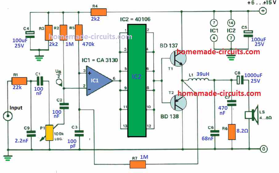
The input audio signal is applied to an op-amp IC1 which functions as a comparator. This setup leads a handful of Schmitt triggers which are connected in parallel to the circuit.
They are there for two reasons. Firstly, there must a “square” waveform and secondly, the adequate base drive current is required for the output stage. In this stage, there are two simple yet fast transistors (BD137/138) installed.
The whole amplifier oscillates and generates a square wave. The reason is one input from the comparator (IC1) is attached to the output through an RC network.
Furthermore, both inputs of IC1 are biased to the first half of the supply voltage by employing a voltage divider R3/R4.
Each time the IC1’s output is low and the emitters of T1/T2 are high, charging of capacitor C3 occurs through resistor R7. At the same time, there will be a rise in voltage at the non-inverting input.
Once this escalating voltage crosses the level of inverting put, the out of IC1 swaps from low to high.
Resultantly, the emitters of T1/T2 turn from high to low. This condition allows C3 to discharge through R7 and the voltage at the plus input dips below the voltage at the minus input.
The output of IC1 also reverts to a low state. In the end, a square wave output is produced at a frequency decided by R7 and C3. The provided values generate an oscillation at 700 kHz.
Using an oscillator, we can modulate the frequency. The inverting input’s level of IC1 which usually is used as a reference does not stay constant but is decided by the audio signal.
Furthermore, the amplitude determines the exact point where the output of the comparator begins to change. Consequently, the “thickness” of the square waves is regularly modulated by the audio signal.
To ensure the amplifier does not operate as a 700 kHz transmitter, filtering must be exercised at its output. An LC/RC network comprising L1/C6 and C7/ R6 does a good job as a filter.
Technical Specifications
- Equipped with a load of 8 ohms and 12 V supply voltage, the amplifier generated 1.6 W.
- When used 4 ohms, the power increased to 3 W. For such small dissipated heat, cooling the output transistors are not required.
- It is proven that the harmonic distortion is unusually low for a simple circuit like this.
- Total harmonic distortion level was lower than 0.32% from the measured range of 20 Hz to 20,000 Hz.
Parts List
Resistors:
R1 - 22k
R2, R7 - 1M
R3, R4 - 2.2k
R6 - 420 k
R6 - 8.2 Ohms
P1 = 100k logarithmic Potentiometer
Conacitor:
C1,C2 - 100 nF
C3 - 100 pF
C4, C5 - 100μF/16 V
C6 =68 nF
C7 - 470nF
C8 - 1000p/10 V
C9 - 2n2
Semiconductors:
IC1 - CA3130
IC2- 00106
T1 =BD137
T2 - BD138
Miscellaneous:
L1 =39μH Inductor
Simple 3 Transistor Class-D Amplifier Circuit
The outstanding efficiency of the PWM amplifier is such that an output of 3 W can be produced with a BC107 used as the output transistor. Even better, it does not require a heatsink.
The amplifier comprises a voltage-controlled pulse width oscillator operating at around 6 kHz and enforcing a class-D output stage.
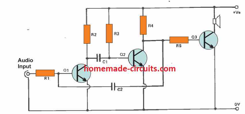
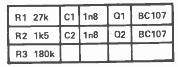

There are only two scenarios – full on or completely off. Due to that, the dissipation is incredibly small and consequently yields high efficiency. The output waveform does not look like the input.
However, the integral of the output and input waveforms are proportional to each other relative to time.
The presented table of component values shows that any amplifier with outputs between 3 W to 100 W can be fabricated. Given that, stronger powers up to 1 kW can be attained.
The disadvantage is that it creates around 30% of distortion. As a result, the amplifier can be utilised for sound amplifying only. It is fit for public address systems due to the speech being incredibly understandable.
Digital Op-Amp
The following concept shows how to use a basic set reset flip flop IC 4013 could be applied for converting analogue audio signal into correponding PWM signal, which can be further fed to a MOSFET stage for the desired PWM amplification.
You may use half of the 4013 package as an amplifier provided a digital output with a duty cycle that is proportional to the desired output voltage. Whenever you need an analogue output, a simple filter would do the job.
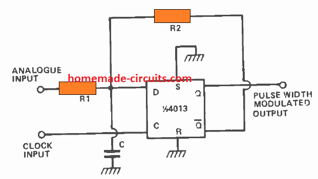
You have to follow the clock pulses as specified and these must be significantly higher in frequency than the desired bandwidth. The gain is R1/R2 whereas the time R1R2C /(R1 + R2) must be lengthier than the clock pulses’ period.
Applications
There are many ways the circuit can be used. Some are:
- Acquire pulses from the zero-crossing point of the mains and enforce a triac with the output. As a result, you now have relational power control without RFI.
- Using a fast clock, switch the driver transistors with the output. The result is a highly efficient PWM audio amplifier.
30 watt PWM Amplifier
A circuit diagram for a 30W Class -D Audio Amplifier can be seen in the following pdf file.
The operational amplifier IC1 amplifies the input audio signal through variable volume controlled potentiometer VR1. A PWM (pulse width modulation) signal is generated by comparing the audio signal with a 100kHz triangle wale. This is accomplished through the comparator 1C6. Resistor RI3 is employed to supply positive feedback and C6 is actually introduced to enhance the comparator operation time.
The comparator output switches between a voltage extremes of ±7.5V. The pull-up resistor R12 offers +7.5V whilst -7.5V is supplied by the op amp IC6's internal open emitter transistor at pin 1. During the time this signal moves to positive level, transistor TR1 works like a current sink terminal. This current sink causes an increase in the voltage drop across resistor R16, which becomes just enough to switch ON MOSFET TR3.
When the signal switches to the negative extreme. TR2 turns into a current source leading to a voltage drop across R17. This drop becomes just sufficient to to turn ON TR4. Basically, MOSFETs TR3 and TR4 are triggered alternately generating a PWM signal that switches between +/-15V.
At this point it becomes essential to bring back or convert this amplified PWM signal into the good audio reproduction which may be an amplified equivalent of the input audio signal.
This is accomplished by creating an average of the PWM duty cycle through a 3rd order Butterworh low-pass filter having a cutoff frequency (25kHz) significantly below the triangle base frequency.
This action leads to huge attenuation at 100kHz. The obtained final output tanspires into an audio output which is an amplified replication of the input audio signal.
The triangle wave generator through the circuit configuration 1C2 and 1C5, where IC2 works like a square wave generator with positive feedback supplied through R7 and R11. Diodes DI to D5 works like a bi-directional clamp. This fixes the voltage to approximately +/-6V.
A perfect integrator is created through preset VR2, capacitor C5 and IC5 that transforms a square wave into a triangle wave. Preset VR2 provides the freqeuncy adjutment feature.
The 1C5 output at (pin 6) supplies feedback to 1C2, and resistor R14 and preset VR3 function as flexible attenuator permitting the level of the triangle wave to be tweaked as required.
After making the full circuit, VR2 and VR3 has to be fine-tuned to enable the highest quality audio output. A set of ordinary 741 op amps for 1C4 and IC3 can be employed as unity gain buffers to supply the +/- 7.5V power.
Capacitors C3, C4, C11, and C12 are used for filtration while the rest of the capacitors are used for decoupling the supply.
The circuit can eb powerede with a dual +/-15V DC power supply, which will be able to drive a 30W 8 ohm loudspeaker through the LC stage using capacitor C13 and inductor L2. Note that modest heatsinks may probably be necessary for MOSFET TR3 and TR4.
PWM Amplifier using Self-Oscillating Concept
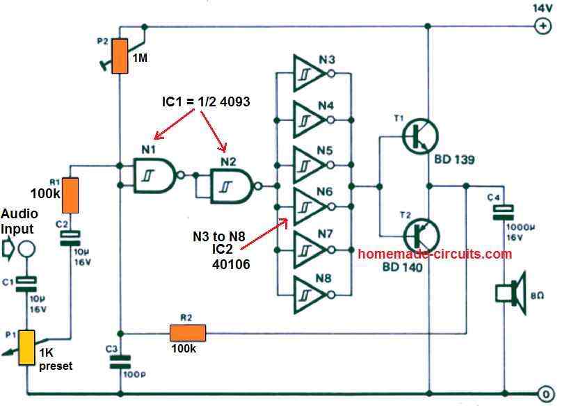
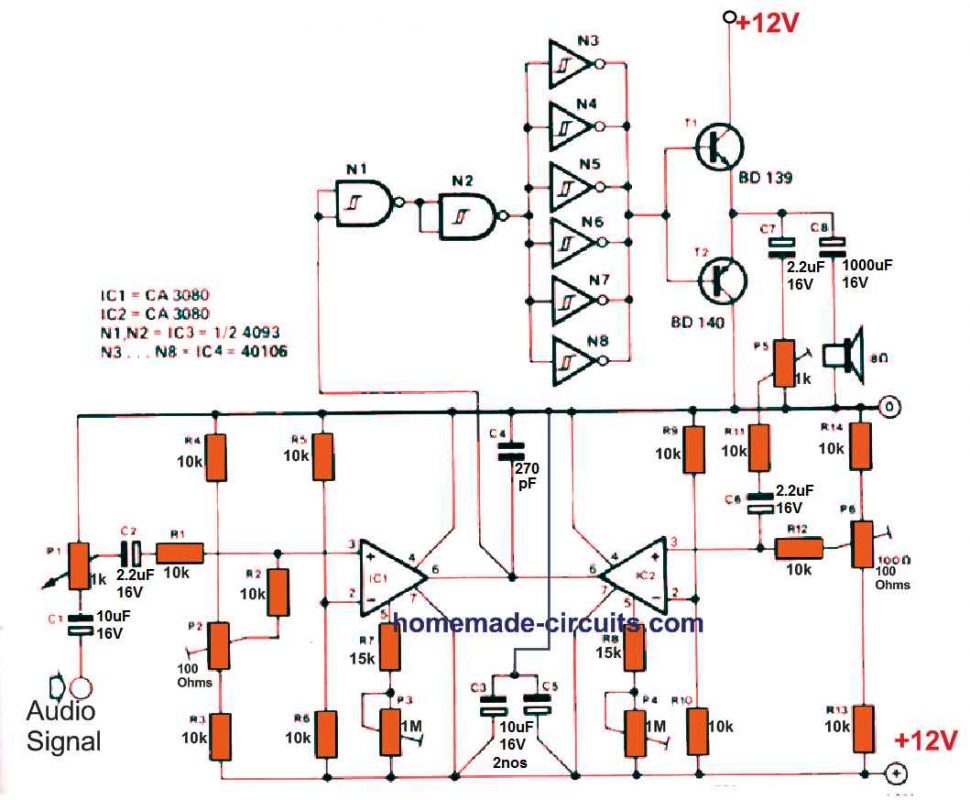
N3 to N8 gates form the comparator, while the two push pull amplifiers form the amplifiers. The buffer inverter N3---N8 gates are connected in parallel to enable greater amplification of the signal from this stage.
Cannot simulate the d flip flop pwm schema
Can you explain better the circuit ?