In this post I have explained a simple 5 V to 10 V converter circuit which can be used in TTL circuits where only 5 V is available and converting this 5 V to 10 V can be extremely useful for operating an adjacent circuit which may require a supply of around 9 V or 12 V.
This voltage doubler circuit can be very handy in circuits which are designed to work with only a 5 V supply voltage, and where a larger voltage is necessary for a different circuit stage.
Circuit Description
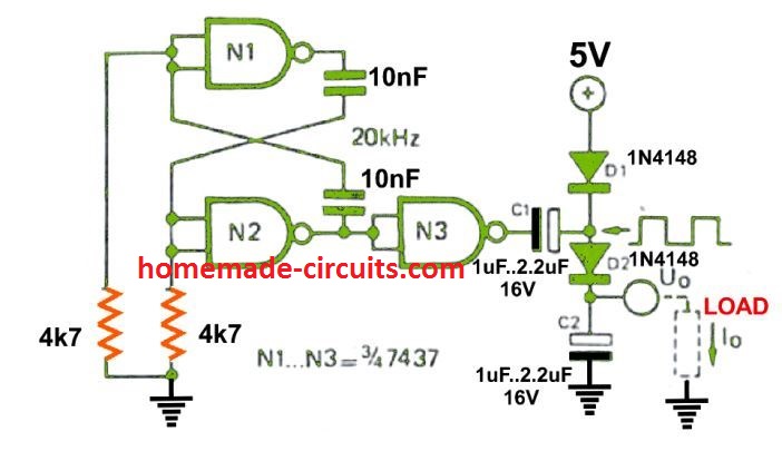
Figure exhibits the fundamental design, that makes use of 3 gates from the IC 7437 quad two-input NAND buffer IC.

Gates N1 and N2 are joined to form a 20 kHz astable multivibrator, and the N2 output runs N3, which behaves like a buffer between the astable and the voltage doubler stages. Once the N3 output is low C1 starts charging up via D1 and N3 to around + 4.4 V.
As soon as the N3 output turns high the voltage over the C1 positive pin becomes 9 V, causing C1 to discharge by means of D2 into C2. In case no current is pulled from C2 it will continue to charge until the voltage across it reaches +8.5 V.
On the other hand, in case any considerable current is utilized by a load, might cause the output voltage to drop rapidly.
Improving Voltage Regulation
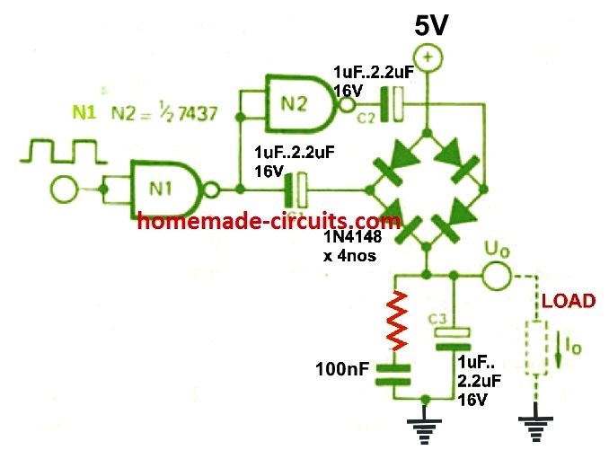
A much improved output voltage regulation, could be achieved by incorporating a push-pull design as shown in the following figure.

This improved 5 V to 10 V converter circuit is driven by a suitable astable square wave source such as from the output of N3 in our previous diagram.
When the N1 output turns low and C1 is in the charging mode, the N2 output becomes high and C2 begins discharging into C3, and vice versa.
Given that C3 is subjected to a continuous charging we find the output voltage regulation much enhanced and stronger than any ordinary voltage doubler variant.
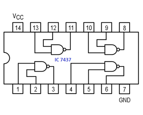
IC 7437 pinout
The following image shows the internal details and pinout configuration of the IC 7437
