These AC to DC power supplies use a single chip to convert mains 220 V or 120 V input AC into 12 V or 5 V DC without depending on a transformer.
Three simple yet efficient 220V single chip based solid state transformerless adjustable solid-state power supply circuits are discussed here.
The first one works using a single IC SR087. The design does not depend on high value capacitors or inductors and yet is capable of delivering 100mA current to the attache load.
WARNING: ALL THE CIRCUITS EXPLAINED BELOW ARE NOT ISOLATED FROM AC MAINS AND THEREFORE ARE EXTREMELY DANGEROUS TO TOUCH IN AN UNCOVERED AND POWERED SITUATION. EXTREME CAUTION IS ADVISED WHILE BUILDING OR TESTING THESE CIRCUITS.
1) Main Features and Board Layout

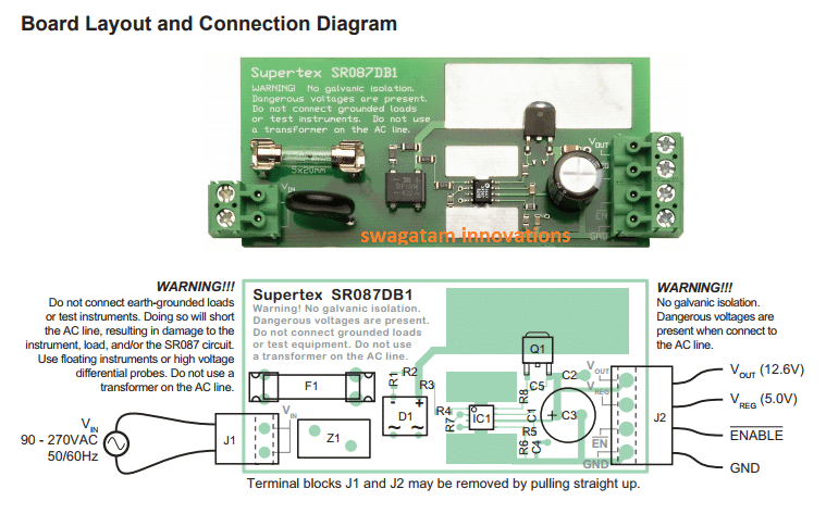
The Main features of this power supply using the IC SR087 are:
High efficiency without incorporating inductors. Does not require high voltage capacitors for mains current dropping. Can be used with 120V AC as well as 220V AC inputs Output adjustable from 9V to 50VDC Has an internal soft stat circuitry Stand by consumption is less than 200mW
The Supertex SR087 is an transformerless switching regulator chip specially designed to operate directly from a rectified 220V or 120V AC line.
The principle of operation is to switch ON a pass transistor each time the rectified AC reaches under the set output level, and switch it OFF as soon as the output level is sustained at the set level.
A internally set 5V linear regulator offers an additional 5V fixed output from the IC for operating devices requiring strict 5V inputs.
The IC also facilitates an external logic input triggered "disable" feature, which can be used for disabling the circuit when not in usee and keep the system in the standby mode.
WARNING! Galvanic isolation is not included in the design. Life threatening voltages and shocks may be floating when switched ON to the AC line. The designer employing the SR087 must ensure proper safety measures are employed to protect the end user from fatality.
The circuits described here are not guaranteed to fulfill surge and EMI conduction requirements.
The working of these circuits might differ depending on a given application. The designer is advised to implement tests to verify compliance with the laid down world standards and regulations.
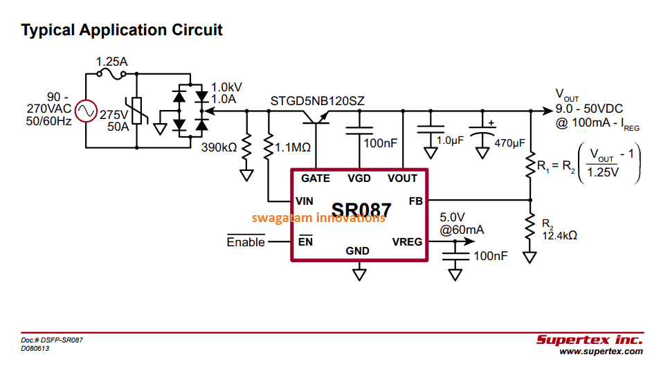
Circuit Diagram
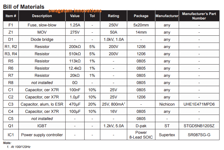
Parts List
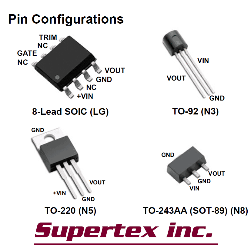
Pinout Description
VIN - Should be connected across a 120/230VAC line. The AC input stgae of the circuit is safeguarded from surge currents by a 275V metal oxide varistor (MOV) and also a 1.25A
slow-blow fuse.
Never use a transformer at the input line. The high inductance might generate an inductive back EMF, overloading the
MOV and destroying it. Please note that the proposed 50V adjustable transformerless power supply is not design to operate through the supply input from a square wave uninterruptible which are also usually referred to as “modified sine wave”.
GND - This is the circuit common line. And because the circuit does not offer a galvanic isolation from mains 220V or 120V, connecting this common line to an earth-grounded equipment,
(such as an oscilloscope), could cause a short circuited the AC line, leading to an instant damage to the circuit or even the equipment in use.
You may also want to note that GND may be at a raised voltage level with respect
to earth ground, even while the AC input is switched off. Be cautioned about this!
VOUT - This refers to the main output of the circuit stage.
The SR087 IC is designed to regulate the peak output voltage, and not the average value, therefore the
average voltage will show a tendency to decline when a load is attached.
VOUT can be adjusted from 9.0 to 50V by changing the value of R1 as per the formula given in the circuit diagram
VREG - It is the fixed 5V regulated output, from the IC. Since this output is derived from the 50V line any load on VREG might cause an equivalent current drop across VOUT.
VREG will require at least 4.0V of headroom
to generate the 5V, that is a minimum of 9V at VOUT.
Since the IC is typically a linear regulator, the SR087 will dissipate
power as curent on VREG output or VOUT goes up to around 460mW at 60mA.
ENABLE - If a logic low (<0.2V) is applied on this pinout it enables Q1
switching and the VOUT switched ON.
However a logic
high (>0.75 • VREG) on this pinout quickly disables Q1
, shutting the VOUT supply and also the VREG output.
However, if an external voltage exists across VOUT terminals in the disabled state, VREG will continue to function allow a 5.0V to be generated across the specified terminals.
The ENABLE input is equipped with 20kΩ pull-down resistor. In case it's not required or unused, it could be simply left unconnected or connected to ground.
2) 12V, 5V Solid-State Power Supply Using IC LR645
In the following second single IC based solid-state design we study how the mains voltage is controlled to 12V and 5V using just a single IC LR645G and some other supportive ordinary active semiconductors.
In one of my earlier posts I provided a similar circuit but it utilized a high voltage capacitor for dropping the mains voltage to lower usable levels.
Thanks to Supertex ic. for providing us with this wonderful little chip LR645G, which single handedly controls any voltage between 24 and 270 V AC and produces DC voltages below 15 volts at the output, which becomes ideally suitable for operating sensitive, compact electronic circuits.
The best part of the circuit is that it does not incorporate any bulky of heavy components like a transformer or non polar high voltage capacitors.
Though we all know the simple way of constructing transformerless power supply units using high voltage capacitors, these high voltage capacitors have one big drawback.
At switch ON, these caps allow high surge inputs to pass through them and also intermediate transients become unstoppable with these devices.
The drawback can cause havoc with any electronic circuit that may be connected to such power supply configurations.
How LR645G Works
Using LR645G the above threat becomes absolutely nullified. The maximum current available from this device is quite low, around 3 mA, however that's never a problem, because the current can be shot up to 150 mA, through a simple addition of an fet DN2540N5 in the circuit.
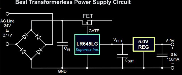
The figure shown above is a classic solid-state circuit set up of a 12V and 5V transformerless power supply circuit which can provide outputs of 15 volts and 5 volts.
15 volts is available just at the junction of the output of LR645 and the input of Ic 7805.
If the 5 volt option is not required, the configuration around the 5 volt regulator can be just eliminated, which makes the circuit yet simpler and compact.
Description
In short the circuit diagram may be understood in the following manner:
- The high voltage AC mains is rectified by the bridge configuration using four diodes at the input.
- The rectified voltage is smoothed by the filter capacitor introduced just after the bridge network.
- The rectified, filtered high voltage is fed to the IC LR645LG, which effectively reduces the voltage to 15 volts at 3 mA.
- The FET pulls the 3 mA current output to 150 mA and feds it to the next stage which incorporates the 5 volt regulator stage.
However one big drawback of not incorporating a transformer is the DANGER of high voltage shock that actively hangs with all the naked points of the circuit.
Therefore extreme caution must be exercised while building and testing this circuit and other attached circuits.
Parts List
- Diodes - 1N4007
- Input Capacitor - 4.7uF/400V,
- Output Capacitors are 1uF/25V
- ICs are LR645LG and 7805,
- FET - DN2540N5
3) Single Chip 0-400V Power Supply Circuit
A cool 0-400V variable transformerless power supply circuit can be built using just a single chip LR8, and a few resistors. The IC features a built in current control stage which makes the design extremely safe even for critical electronic circuits.
How LR8 IC is Designed to Work
The IC LR8 is quite similar to our very own LM317 or LM338 ICs except their maximum input voltage and the current delivering capacity specs which are wide apart, rest of the attributes are exactly similar.
Since the IC LR8 is designed to work with huge voltages upto 430V, its current handling capacity is consequently much lower at 20mA maximum, but nevertheless, at 400V this current could appear significantly useful.
Since the proposed 0-400V transformerless power supply circuit is rated to work with over 400V AC, implies that this circuit could be simply plugged in with our mains socket directly without having to worry about surge inrushes, or other related catastrophic situations.
How it Works
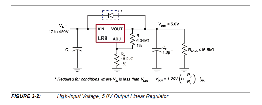
Referring to the circuit design of the 0-400V transformerless power supply above, we can see that it is exactly identical to the LM317 type voltage regulators, where R1 is used for setting up the reference voltage for the ADJ pin, while R2 is positioned for determining the intended output voltage across C2.
In the diagram the 18K resistor is supposed to produce a precise 5V at the output as long as the input voltage is 12V above the output value....meaning for acquiring 5V the minimum input supply voltage should be 17V.
Similarly for ensuring a minimum 1.25V at the output, the input source will need to be around 13.2V. In short the differential voltage needs to be +12V over the desired output value.
For acquiring a smooth variable 0-400V or 0-300V DC output from a 220V mains rectified input source, the R2 could be replaced with a 100K pot.
For other fixed values the specified formula could be utilized as suggested in the diagram.
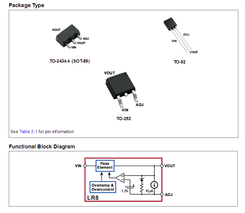
The pinout diagram for the LR8 IC can be learned from the following image:
Now since you know how to build a 0-400V transformerless power supply circuit, how do you plan to use it for your specific need?....think, and share if possible through the comment box.
Instead of “mains”, why not adapt this to DC input of 5V directly (from standard micro-device wall charger such as for a cell phone, via a USB male connector? Precision would be better for a stable current draw (say 1.5VDC @ 500mAh). My use is for a NIST reference atomic clock that runs (now) on 3×1.5 “C” (LR14) cells. Typical wall bricks have too much voltage / current variation and eventually lead to premature device failure.
With a DC input supply you can simply use voltage regulators ICs such as a 7805.
https://www.homemade-circuits.com/how-to-understand-and-use-voltage/
Sir
Instead of capacitor reactance i thinks Supertex inc. device is great choice.
My mcu base circuit need 5 v @ max 10ma . which is best choice for me LR8 OR LR 645LG ?
Does it reliable and sturdy up to work with min 2 years ? Have u know ?
Nitesh, all the circuits shown above are very reliable and will work for years, any one of these can be selected depending on the load specifications.
thanks sir for prompt reply. Once again highly satisfied with answer.
You are welcome Nitesh!
this all circuit is isolated with the mains ?
No it isn’t
Hi Swagatam,
what a great valuable information thanks for are sharing with community, i have been reading through your different section in you blog, as i’m looking for SMPS/transformerless/non-isolated PSUs, i’m have a very limited footprint (25mm x 15mm double layers) on my IOT little device and seeking a 500mA to drive 2 relays(5v) and an ESP chip (3.3v).
i like the SMPS shown above in this post but i wonder if i can get the required current with such simple (no inductors) circuits,
i also considered your capacitive high current transformer-less circuits in different posts, which direction would you recommend
Thank you Ahmed, I think the first smps design from the following article can be a good choice for your requirement.
https://www.homemade-circuits.com/how-to-make-simplest-1-watt-led-driver/
You can customize the coil to get 5 V 500 mA
Hello,
I am wondering what the value and purpose of the input capacitor C1 on the LR8 example application circuit should be ? What kind of capacitor should be used ?
I am planning to use such circuit for powering a microcontroller-based system which will not pull more than 10mA.
It is a filter capacitor can be any value in uF, and rated at 400V
Sir I need a transformerless power supply of abt 12 – 15v 10amps.
sorry, 10 amp smps is not available with me at the moment