As the name suggests, an inverter circuit that converts a DC input into AC without depending on an inductor or a transformer is called a transformerless inverter.
Since an inductor based transformer is not employed, the input DC is normally equal to the peak value of the AC generated at the output of the inverter.
The post helps us to understand 3 inverter circuits designed to work without using a transformer, and using a full bridge IC network and a SPWM generator circuit.
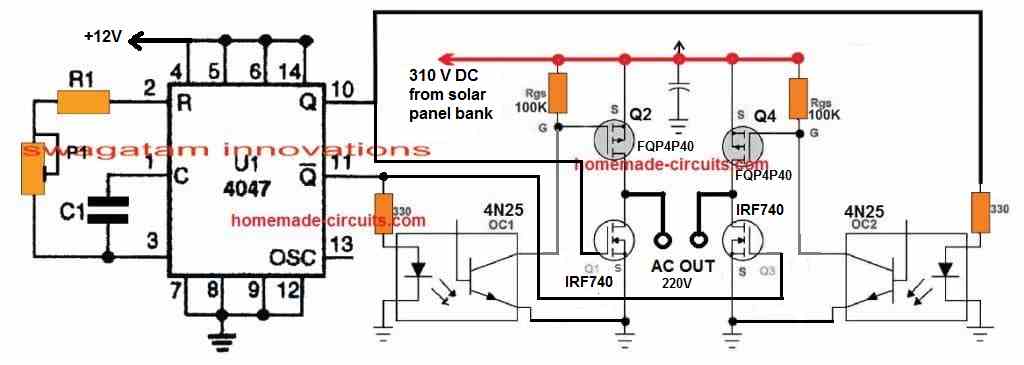
Transformerless Inverter using IC 4047
Let's begin with an H-Bridge topology that's probably the simplest in its form. However, technically it's not the ideal one, and not recommended, since It is designed using p/n-channel mosfets. P-channel mosfets are used as the high side mosfets, and n-channel as the low side.
Since, p-channel mosfets are used on the high side, the bootstrapping becomes unnecessary, and this simplifies the design a lot. This also means this design does not have to depend on special driver ICs.
Although the design looks cool and enticing, it has a few underlying disadvantages. And that's exactly why this topology is avoided in professional and commercial units.
That said, if it's built correctly may serve the purpose for low frequency applications.
Here's the complete circuit using IC 4047 as the astable totem pole frequency generator

Parts List
All resistors are 1/4 watt 5%
- R1 = 56k
- C1 = 0.1uF / PPC
- IC pin10/11 resistor = 330 ohms - 2nos
- MOSFET gate resistors = 100k - 2nos
- Opto-couplers = 4N25 - 2 nos
- Upper P-channel MOSFETs = FQP4P40 - 2nos
- Lower N-Channel MOSFETs = IRF740 = 2nos
- Zener diodes = 12V, 1/2 watt - 2 nos
The next idea is also an h-bridge circuit but this one uses the recommended n-channel mosfets. The circuit was requested by Mr. Ralph Wiechert
Main Specifications
Greetings from Saint Louis, Missouri.
Would you be willing to collaborate on an inverter project? I would pay you for a design and/or your time, if you'd like.
I have a 2012 & 2013 Prius, and my mother has a 2007 Prius. The Prius is unique in that it has a 200 VDC (nominal) high-voltage battery pack. Prius owners in the past have tapped into this battery pack with off-the-shelf inverters to output their native voltages and run tools and appliances. (Here in the USA, 60 Hz, 120 & 240 VAC, as I'm sure you know). The problem is those inverters are no-longer made, but the Prius is still is.
Here are a couple inverters that were used in the past for this purpose:
1) PWRI2000S240VDC (See attachment) No longer manufactured!
2)Emerson Liebert Upstation S (This is actually a UPS, but you remove the battery pack, which was 192 VDC nominal.) (See attachment.) No longer manufactured!
Ideally, I'm looking to design a 3000 Watt continuous inverter, pure sine wave, output 60 Hz, 120 VAC (with 240 VAC split phase, if possible), and transformer-less. Perhaps 4000-5000 Watts peak. Input: 180-240 VDC. Quite a wish-list, I know.
I am a mechanical engineer, with some experience building circuits, as well as programming Picaxe micro-controllers. I just don't have much experience designing circuits from scratch. I'm willing to try & to fail, if needed!
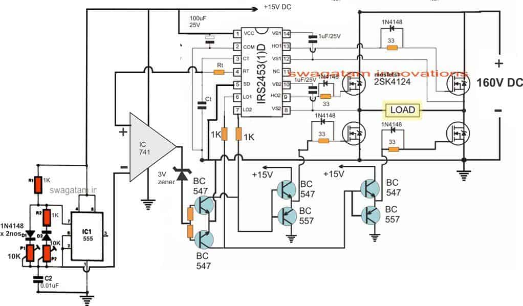
The Design
In this blog I have already discussed more than 100 inverter designs and concepts, the above request can be easily accomplished by modifying one of my existing designs, and tried for the given application.
For any transformerless design there has to be a couple of basic things included for the implementation: 1) The inverter must be a full bridge inverter using a full bridge driver and 2) the fed input DC supply must be equal to the required output peak voltage level.
Incorporating the above two factors, a basic 3000 watt inverter design can be witnessed in the following diagram, which has a pure sinewave output waveform feature.
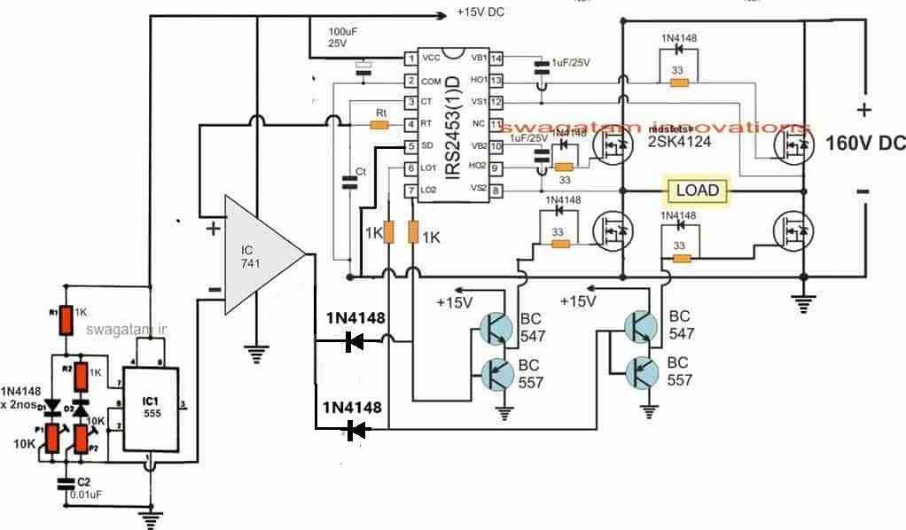
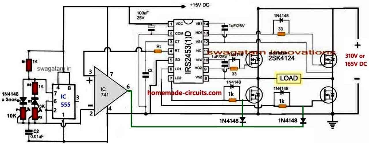
The above diagram can be further simplified as shown in the following figures:
The functioning details of the inverter can be understood with the help of the following points:
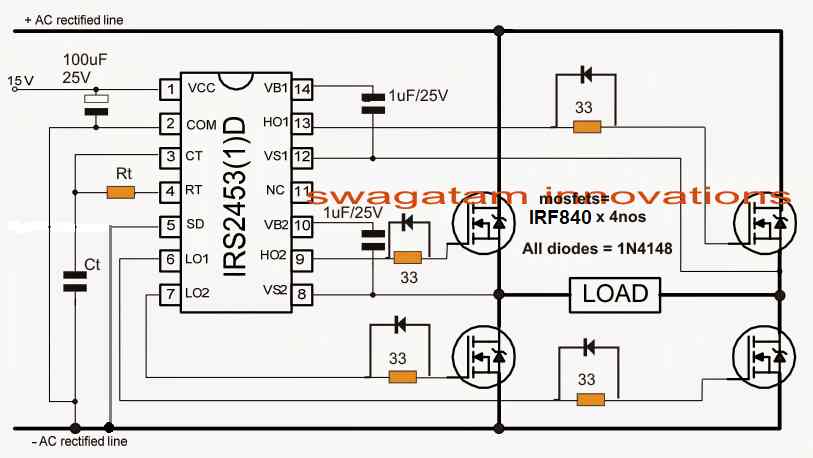
The basic or the standard full bridge inverter configuration is formed by the full bridge driver IC IRS2453 and the associated mosfet network.
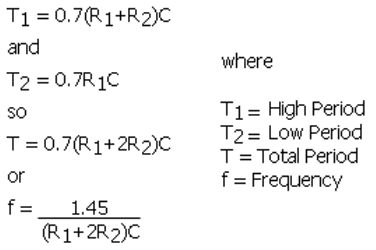
Calculating the Inverter Frequency
The function of this stage is to oscillate the connected load between the mosfets at a given frequency rate as determined by the values of the Rt/Ct network.
The values of these timing RC components can be set by the formula: f = 1/1.453 x Rt x Ct where Rt is in Ohms and Ct in Farads. It should be set for achieving 60Hz for complementing the specified 120V output, alternatively for 220V specs this could be changed to 50Hz.
This may be also achieved through some practical trial and error, by assessing the frequency range with a digital frequency meter.
For achieving a pure sinewave outcome, the low-side mosfets gates are disconnected from their respective IC feeds, and are applied the same through a BJT buffer stage, configured to operate through an SPWM input.
Generating SPWM
The SPWM which stands for sinewave pulse width modulation is configured around an opamp IC and a single IC 555 PWM geneartor.
Although the IC 555 are configured as PWM, the PWM output from its pin#3 is never used, rather the triangle waves generated across its timing capacitor is utilized for the carving of the SPWMs.
Here one of the triangle wave samples is supposed to be much slower in frequency, and synchronized with the main IC's frequency, while the other needs to be faster triangle waves, whose frequency essentially determines the number of pillars the SPWM may have.
The opamp is configured like a comparator and is fed with triangle wave samples for processing out the required SPWMs. One triangle wave which is the slower one is extracted from the Ct pinout of the main IC IRS2453
The processing is done by the opamp IC by comparing the two triangle waves at its input pinouts, and the generated SPWM is applied to the bases of the BJT buffer stage.
The BJTs buffers switch according to the SPWM pulses and make sure that the low side mosfets are also switched at the same pattern.
The above switching enables the output AC also to switch with an SPWM pattern for both the cycles of the AC frequecny waveform.
Selecting the mosfets
Since a 3kva transformerless inverter is specified, the mosfets need to be rated appropriately for handling this load.
The mosfet number 2SK 4124 indicated in the diagram will actually not be able to sustain a 3kva load because these are rated to handle a maximum of 2kva.
Some research on the net allows us to find the mosfet: IRFB4137PBF-ND which looks good for operating over 3kva loads, due to its massive power rating at 300V/38amps.
Since it is a transformerless 3kva inverter, the question of selecting transformer is eliminated, however the batteries must be appropriately rated to produce a minimum of 160V while moderately charged, and around 190V when fully charged.
Automatic Voltage Correction.
An automatic correction can be achieved by hooking up a feedback network between the output terminals and the Ct pinout, but this may be actually not required because the IC 555 pots can be effectively used for fixing the RMS of the output voltage, and once set the output voltage can be expected to be absolutely fixed and constant regardless of the load conditions, but only as long as the load does not exceed the maximum power capacity of the inverter.
2) Transformerless Inverter with Battery Charger and Feedback Control
The second circuit diagram of a compact transformeress inverter without incorporating bulky iron transformer is discussed below. Instead of an heavy iron transformer it uses a ferrite core inductor as shown in the following article.
The schematic is not designed by me, it was provided to me by one of the avid readers of this blog Mr. Ritesh.
The design is a full fledged configuration with includes most of the features such as ferrite transformer winding details, low voltage indicator stage, output voltage regulation facility etc.
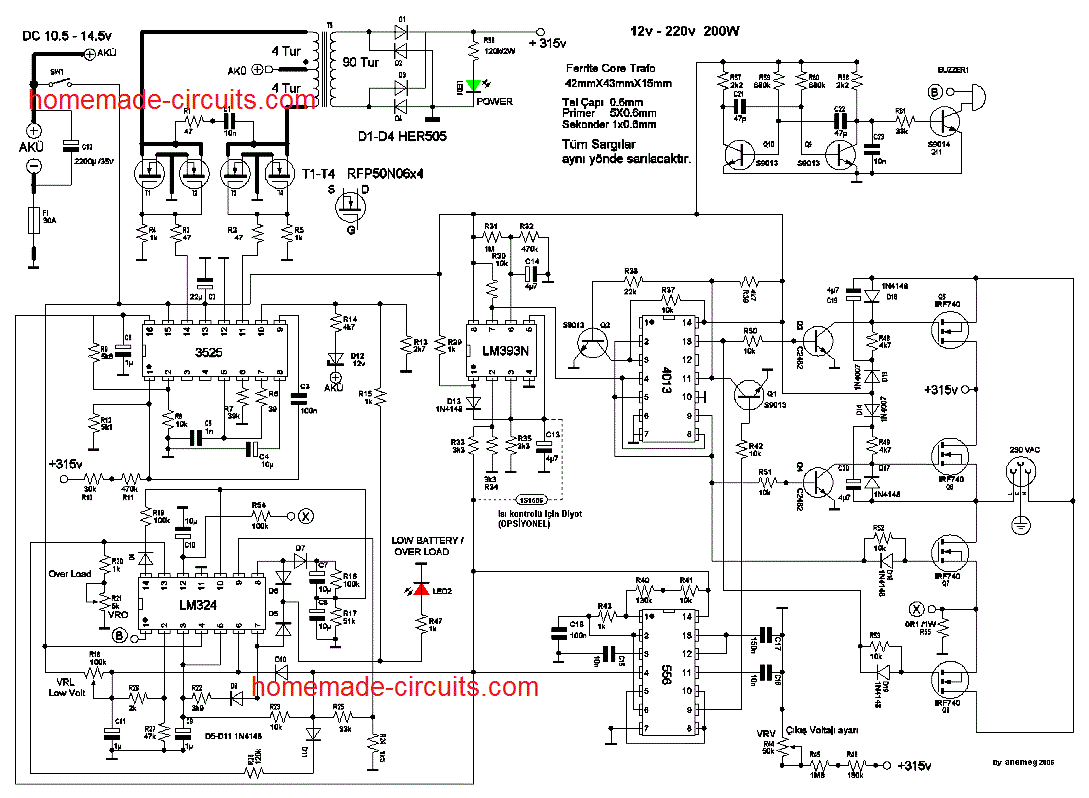
The explanation for the above design hasn't been updated yet, I will try to update it soon, in the meantime you can refer the diagram and get your doubts clarified through comment, if any.
200 watt Compact Transformerless Inverter Design#3
A third design below shows a 200 watt inverter circuit without a transformer (transformerless) using a 310V DC input. It is a sine wave compatible design.
Introduction
Inverters as we know are devices which convert or rather invert a low voltage DC source to a high voltage AC output.
The produced high voltage AC output is generally in the order of the local mains voltage levels. However the conversion process from a low voltage to high voltage invariably necessitates the inclusion of hefty and bulky transformers. Do we have an option to avoid these and make a transformerless inverter circuit?
Yes there is a rather very simple way of implementing a transformerless inverter design.
Basically inverter utilizing low DC voltage battery require to boost them to the intended higher AC voltage which in turn makes the inclusion of a transformer imperative.
That means if we could just replace the input low voltage DC with a DC level equal to the intended output AC level, the need of a transformer could be simply eliminated.
The circuit diagram incorporates a high voltage DC input for operating a simple mosfet inverter circuit and we can clearly see that there's no transformer involved.
Circuit Operation
The high voltage DC equal to the required output AC derived by arranging 18 small, 12 volt batteries in series.
The gate N1 is from the IC 4093, N1 has been configured as the oscillator here.
Since the IC requires a strict operating voltage between 5 and 15 volts,the required input is taken from one of the 12 volt batteries and applied to the relevant IC pin outs.
The entire configuration thus becomes very simple and efficient and completely eliminates the need of a bulky and heavy transformer.
The batteries are all 12 volt, 4 AH rated which are quite small and even when connected together does not seem to cover too much of space.They may stacked tightly to form a compact unit.
The output will be 110 V AC at 200 watts.
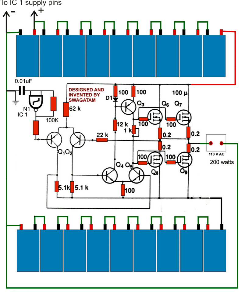
Parts List
- Q1, Q2 = MPSA92
- Q3 = MJE350
- Q4, Q5 = MJE340
- Q6, Q7 = K1058,
- Q8, Q9 = J162
- NAND IC = 4093,
- D1 = 1N4148
- Battery = 12V/4AH, 18 nos.
Upgrading into a Sinewave Version
The above discussed simple 220V transformerless inverter circuit could be upgraded into a pure or true sinewave inverter simply by replacing the input oscillator with a sine wave generator circuit as shown below:
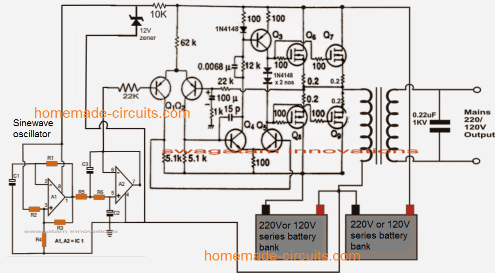
Parts List for the sinewave oscillator can be found in this post
Transformerless Solar Inverter Circuit
Sun is a major and an unlimited source of raw power which is available on our planet absolutely free. This power is fundamentally in the form of heat, however humans have discovered methods of exploiting the light also from this huge source for manufacturing electrical power.
Overview
Today electricity has become the life line of all cities and even the rural areas. With depleting fossil fuel, sun light promises to be one of the major renewable source of energy that can be accessed directly from anywhere and under all circumstances on this planet, free of cost. I have explained one of the methods of converting solar energy into electricity for our personal benefits.
In one of my previous posts I have discussed a solar inverter circuit which rather had a simple approach and incorporated an ordinary inverter topology using a transformer.
Transformers as we all know are bulky, heavy and may become quite inconvenient for some applications.
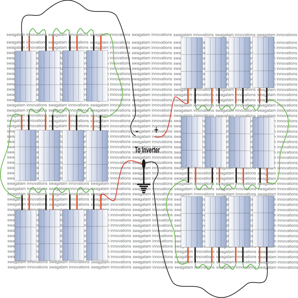
In the present design I have tried to eliminate the use of a transformer by incorporating high voltage mosfets and by stepping up the voltage through series connection of solar panels. Let's study the whole configuration the with the help of the following points:
How it Works
Looking at the below shown solar based transformerless inverter circuit diagram, we can see that it basically consists of three main stages, viz. the oscillator stage made up of the versatile IC 555, the output stage consisting of a couple of high voltage power mosfets and the power delivering stage which employs the solar panel bank, which is fed at B1 and B2.
Circuit Diagram
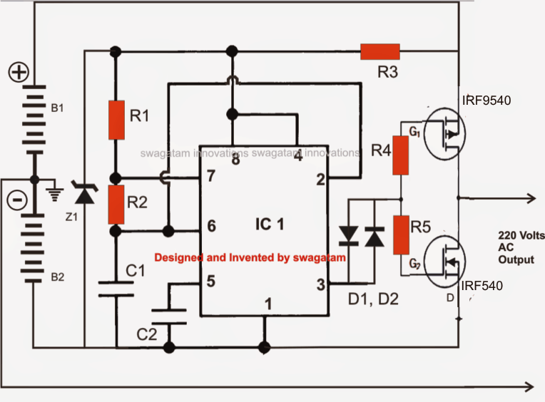
Since the IC cannot operate with at voltages more than 15V, it is well guarded through a dropping resistor and a zener diode. The zener diode limits the high voltage from the solar panel at the connected 15V zener voltage.
However the mosfets are allowed to be operated with the full solar output voltage, which may lie anywhere between 200 to 260 volts. On overcast conditions the voltage might drop to well below 170V, So probably a voltage stabilizer may be used at the output for regulating the output voltage under such situations.
The mosfets are N and P types which form a pair for implementing the push pull actions and for generating the required AC.
The mosfets arenot specified in the diagram, ideally they must be rated at 450V and 5 amps, you will come across many variants, if you google a bit over the net.
The used solar panels should strictly have an open circuit voltage of around 24V at full sunlight and around 17V during bright dusk periods.
How to Connect the Solar Panels
Parts List
R1 = 6K8
R2 = 140K
C1 = 0.1uF
Diodes = are 1N4148
R3 = 10K, 10 watts,
R4, R5 = 100 Ohms, 1/4 watt
B1 and B2 = from solar panel
Z1 = 5.1V 1 watt
Use these formulas for calculating R1, R2, C1....
Update:
The above 555 IC design may not be so reliable and efficient, a much reliable design can be seen below in the form of a full H-bridge inverter circuit. This design can be expected of providing much better results than the above 555 IC circuit.
Another advantage of using the above circuit is that you won't require a dual solar panel arrangement, rather a single series connected solar supply would be enough to operate the above circuit for achieving a 220V output.
These transformerless inverter circuit components can they be found for purchase and work perfectly ?
I would recommend the following design:
" rel="ugc">
If implemented step-wise, with proper understanding, it will work as intended.
Hello
Do you know if there is a circuit schematic I can get that would show me how to build a 20 kw 220 vac split phase inverter 48-volt dc supply
Hi,
I don’t have this circuit with me right now, but it is not difficult to design one. I will do it soon and post it in this blog as a new article.
Dear Sir,
Can I use Fairchild 41N60E?
Rds 41mohms
VDs600
ID77
Input capacitance 13000pf
Qg385nc
Yes, you can use it.
Hi Sir,
As I apply 175v AC which after filter became 175*1.4=245vdc, I have applied 1u 400 volt polyester capacitor between the highside source pin that means between the load. I also uses irfp264n mosfets which is 250 vDC with 44amp rated.
When I apply power the 1u capacitor became leaked and a liquid substance drowning from its body and the line MCB cutoff when I forcefully on the MCB then a blast occurred at the MOSFET high side drain pin with black charge spot on the pcb, all the MOSFET are dead.
I also observed when I apply 25vdc power at the MOSFET then the output gives 25v AC but when I Apply 110volt DC then the output voltage fluctuates as 47, 97,109 vac and when 245vdc given the output became 570,289,330 as well as input also fluctuates.
Hi Rinku,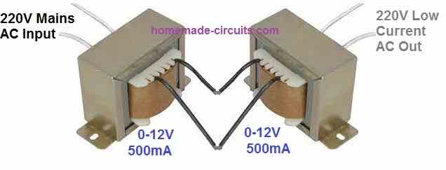
If your supply voltage is 250V then the MOSFETs must be rated at least 300V or ideally 500V.
https://www.vishay.com/docs/91070/91070.pdf
Your 1uF capacitor could be faulty or not rated to handle 250V. Try a good quality PPC 105/400V capacitor.
If you supply 250V to the H-bridge, the output will also be 250V, it cannot fluctuate between 570V or 289V. If this happening, it is due to your meter instability, and due to high inverter frequency.
Make sure the inverter frequency is 50Hz.
Always connect a fuse in series with the supply.
For initial testing you can use a low current AC supply through transformer connected in the following manner.
" rel="ugc">
Good morning Sir,
As per above link I have added three transformer to achieve 100 volt AC which after filter became 138vdc and 100 watt bulb filament glowing red as we observe when our domestic line became single phase.
My spwm signal output at 4500Hz
Output load frequency is at 50.03Hz with sinewave pulse.
The output frequency have measured when I gave 25volt supply. I have not tested it with 220 vac or 110 vdc..
But I have measured direct 220 AC wave form which is similar to that of 25 volt wave form I supplied to mosfets.
Rinku, since the transformer current is low, you can try a 25 watt or a 10 watt bulb as the load.
Rest everything looks OK to me at the moment.
Good morning Sir,
Have question regarding testing the full bridge inverter.
As I have no solar panel at this moment I tried connecting a stabilizer 175volt tapping with a 35 amp bridge rectifier supplying 210vdc, the output is connected 100watt 230volt bulb when I apply AC current the bulb glows fully but the stabilizer fuse immediately blown up.
The 12 volt is supplied through a 12 volt adaptor separately though no inverter parts are damaged yet
Hello Rinku,
Try with a 40 watt bulb, and check whether the fuse blows or not. I think the fuse is not rated to handle 100 watts.
Hi Sir,
But the stabilizer is serving my refrigerator which is operated by 120 watt compressor
If there was a short circuit in the h-bridge, the bulb would never glow, but since the 100 watt bub is glowing that means the h-bridge is working ok.
Still i would recommend checking with a 40 watt bulb, if there’s a short circuit the fuse would blow again.
Hi Sir,
I connected the 1000ufd 400 volt capacitor to DC line and the fuse blown immediately but when I remove the positive connection then it ok.
Hi Rinku, When you switch ON power the 1000uF acts like a momentary short circuit, until it charges fully, this momentary short circuit could be causing the fuse to blow. Try a 10 ohm or 20 ohm resistor in series with the 1000uF and check.
Or use an NTC thermistor in series with the supply, that might help.
Dear sir,
Please elaborate this issue and enlighten me what happens here when punching SPWM signal to lowside mosfets,why should we use reverse diode? If I use 1 k resistor between pin 6&7 (2453ic) and gates and connect the spwm with two forward diode directly to gates the gate voltage is 7.8 and 8.1 volt respectively
The spwm & triangle generated by lm 324 is great and spwm output is 3.45volt
Hi Rinku,
You can use 1k resistor as the gate resistors for the low side MOSFETs but do not forget to add the parallel diodes across these 1k resistors, otherwise the low side MOSFETs might heat up.
The idea is to chop each 50 Hz square wave pulse at the low side MOSFFET gates into pieces replicating the SPWM waveform. So we want to create the notches or the OFF periods on these 50 Hz pulse which are exactly similar to the SPWM pulse notches.
Notches are the gaps that are present in our SPWM cycles.
During these notch periods or the OFF periods of the SPWM, the 50 Hz cycles are pulled to ground through the reverse 1N4148 diodes, into the 741 IC pin6 creating a similar off period on the 50 Hz cycles, at the MOOSFET gate.
So whenever we have the off periods in the SPWM, the 50Hz pulse on the gate are pulled to ground through the diodes and the 741 pin#6 which causes identical off periods to be carved in those 50 Hz gate pulses.
To enable the off periods to react on the 50Hz pulses we need reverse diodes only, the forward diodes would block these off periods so we cannot use forwards diodes.
Dear Sir,
Please tell me which one is correct or both are wrong
https://quickshare.samsungcloud.com/aBaFstfHFyhc
Hi Rinku, both are wrong, the SPWM can be replicated at the low side gates only with negative pulses, and that is why the diodes needs to be reverse biased and not forward biased. If you use forward biased diodes it will have no effect on the MOSFET gates.
I have explained you in the earlier comment regarding how the diodes work.
Hello Sir,
So final result is, if the spwm reverse diode connection is open then the signal can be measured with respect to +12 volt and if reverse diode connected directly with gates then no signal can be measured with respect to positive or negative only 50 Hz pulse will reflect.
Yes, If the spwm is connected with the gates through reverse diodes, then you can measure the gate waveform by attaching the scope probes across the gate/source of the mosfets.
Dear Sir,
Below is the comparison of ct pin 3 of 2453ic and spwm at 741 output
https://quickshare.samsungcloud.com/csKiCFtxcNSZ
This diagram is much better and clearly shows the spwm in response to the slow triangle waves from the CT pin of the inverter IC. The spwm output from ic 741 is confirmed now.
Good afternoon Sir,
Below is the spwm out from 741 with respect to ground
https://quickshare.samsungcloud.com/jlEj0Ur97PLa
Hello Rinku, the full spwm cycle is not visible in this image, so I cannot confirm it.
Dear Sir,
Apologi to disturb you again
The channel 2 showing spwm output of 741 and channel 1 showing high side source between/load frequency
https://quickshare.samsungcloud.com/fQoZBQAKFj8Z
Diode have removed from 741 output added 1 k resistor to base of bjt buffer with 220R ground
Hello Rinku, The SPWM is not clear, that is why had I told you to first confirm the SPWM from IC741 before integrating with the low side MOSFETs.
Please disconnect the pin#6 of 741 from the inverter circuit.
Check the SPWM between pin#6 of 741 and ground. For each triangle wave pulse from the CT pin of IRS2453 there should one set of SPWM generated at pin#6 of IC 741.
Only after confirming the above, integrate the 741 output with the low side MOSFETs in the following manner: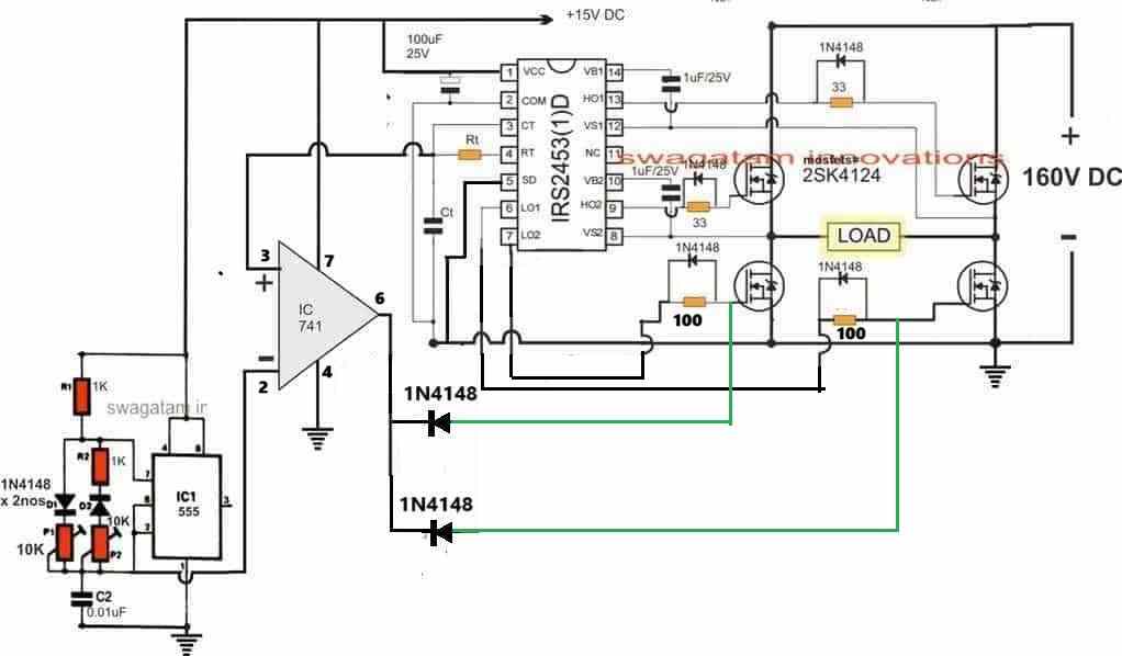
" rel="ugc">
Remember to change the low side gate resistor to 100 ohms and USE REVERSE 1N4148 DIODES PARALLEL TO THE GATE RESISTORS, as shown in the diagram.
Good morning Sir,
Below is the pin6 wave form of ic 741
https://quickshare.samsungcloud.com/eF9DLcvxOTEB
This waveform is valid only at the cathode of diode when the MOSFET vds voltage is applied and if the supply voltage is discontinued then it reflect to gate of lowsides mosfets while the 12 volt is supplied to ic 741,555&2453
So what is the reason when MOSFET vdd given frequency disappear from gate and while supply disconnect and bulb is off then the spwm signal appears.
What’s the reason?
I am frustrated
Hi Rinku,
I can only help you to understand the circuit and implement it, I cannot troubleshoot your circuit because I cannot practically check it. If I could check your circuit I could quickly solve it for you.
Please understand the working of the SPWM and if you have understood it, implement it accordingly.
The positive peaks of the SPWM will have no effect on the totem pole base and therefore have no effect on the gate of the low side MOSFETs,
However, the negatives of the SPWM which are in the form of valleys or gaps, will turn OFF the BC547 BJT and the gate voltage of the low side MOSFET, in this way it will chop the low side MOSFET gate and force the H-Bridge to oscillate with the SPWM pattern. This will create the intended sine wave output on the load.
Are you building this circuit on breadboard? If yes then please build it on a strip board by soldering.
Your SPWM image looks somewhat OK, but I cannot see the full start to end of the waveform, please make the range smaller and try to get at least two consecutive cycles of the SPWM.
Good morning Sir,
As per your instructions I have measured the frequency and it is bunch of 5 bars but the output I measured connected both probe at source of each highside mosfets it shows neat and clean 50 Hz with 50% duty cycle frequency and if I detach one probe with remaining at one probe at source and the other with output of 741 then it shows nice sinewave picture, I just touch the output and detach it and this is the result.
Please guide me
The bulb glow at full with 21 volt AC
This voltage cannot measure in the DC range of my multimeter
Regards
Good Morning Rinku,
Please confirm the spwm waveform across the pin#6 of ic 741 and ground, across gate/source of the low side MOSFETs. Finally, confirm the above between the sources of the upper two high side mosfets. If your oscilloscope shows the spwm waveform correctly across the above sections that would confirm the sine wave working of the inverter. Remember, to get a pure sinewave you will need a transformer across the h-bridge output.
Hi Engineer Sir,
Can I operate this load terminal directly with any electrical machines or it will require a transformer such as voltage stabilizer transformer through which I can run motor, fans etc, as this is a transformer less inverter will it requires a stepup transformer or you recommend a stepdown transformer to measure the frequency only whether it produce sinewave or not.
Hi Rinku,
You can connect a load directly across the load terminals, no need of a transformer. But if you use 12V DC as the supply and use a 12V to 220V transformer across the load terminals then that will help you to generate a pure sine wave 220V output.
Dear Sir,
It means if I use solar 160vdc as input I cannot make it pure sine wave then how to get pure sinewave if I use solar series power as my input, in that case which transformer I can use to convert it sinewave? If I use transformer the efficiency of inverter will be hampered,it will give only 65%
Hi Rinku, you can get a pure sinewave even without a transformer. How much pure the sinewave can be depends upon how many pillars you use inside each spwm waveform. You can increase the frequency of the fast triangle waves in order to increase the number of pillars inside each spwm….The more numbers you have the better will be the purity of the sine waveform.
Yes Engineer that’s the solution I want to hear from you as you wrote in this edition about 330Hz frequency limitation I can’t go to test for higher frequency because if it blown the mosfets. If I apply 1kHz spwm signal then the ratio would be 1:20 , will the mosfets remain live?
Another question please clarify::
The pin 6&7 of 2453 ic giving 6 volt mean and pk to 12 volt when I add diode to output of 741 ic the voltage became half why this happens?
MOSFETs can handle frequencies in GHz, so increasing frequency in kHz will not blow a MOSFET, unless there’s some other reasons.
330Hz is recommended if an iron core transformer is used at the output, otherwise not.
Yes, the SPWM will reduce the conduction rate by around 50%, that is why your seeing 50% drop in the pin6/7 voltages, but the peak will be 12V
Hi Sir,
Good evening, the diode you have used in your modified transformerless inverter 741opamp output to pass signal to totempoll base is not giving any spwm signal as voltage cannot passes through cathode of diode similarly signal also blocked by the diode 4148,so what should we do to carry the signal,if we direct the output to base of totem it will damage the mosfets as well the 2453 ic as high current pass through.
I have connected 10 k resistor from 741output to bjt base with grounding it by 1 k resistor and the low side gate voltage (mean) is 3.7v .but as I supply power to mosfet the magnitude of signal decreases.
Please solve this problem
Hi Rinku, the output from the diode is supposed to be negative, not positive, so you can check the SPWM across the diode output and the positive line.
First of all is your basic inverter working without the 741 SPWM, remember I told you to confirm that first?
Also, are you using an oscilloscope to confirm the SPWM. Without an oscilloscope it is impossible to check and troubleshoot this inverter circuit.
If you don’t have an oscilloscope you can buy the following one:
https://www.homemade-circuits.com/dso138-best-small-oscilloscope-for-electronic-hobbyists/
Hi Sir,
The primary circuit is working fine without the 741,there is no voltage drop at the load output.
I am measuring the diode frequency with respect to ground as the voltage is negative as you are saying, so where my scope will display the frequency?
So I have to measure it with respect to positive voltage
One probe should be connected with anode of diode and the other with +VCC.
Yes, that’s right, you have to check the 741 output in that manner….but the waveform is most important, you must confirm whether you are getting the exact spwm waveform or not.
Yes Sir,
How many tricks have to learn from you to discover this transformerless inverter, God knows
Good evening Sir,
Please tell me about parameters of SPWM wave i.e. the time division and voltage division and duty cycle so that I can match it with my scope.
Thanks for your support
Goodnight
Rinku
Hello Rinku, the SPWM should look like this:
" rel="ugc">
Hi Engineer,
I am facing problem with HO2 MOSFET which blown twice with casualty of 2453 ics HO1 voltage absence and pin14 capacitor not charging but remaining part of ic is ok,, This happened because I modify the totem driver with 3.3 volt zener with 10k resistor as the diode (your modified circuit) connected to totem doesn’t carry the spwm signal(very low) to the lowside. Now the 741 out signal is 330Hz and totempoll output is 268 HZ,How should I protect the ic from reverse current? Should I change the highside diode direction from reverse to forward and apply a gate source NPN transistor to catch the reverse current, but here is one major drawback that the gate voltage never became zero.
Plz give your valuable comment.
শুভ রাত্রি
রিঙ্কু
Hi Rinku,
You must build the inverter in a step by step manner.
First build the basic square wave inverter without the IC 741 and the IC555 and without the totem pole transistor stage. Connect the LO1 and LO2 directly to the low side mosfet gates though the 33 ohms resistors.
If you succeed, then try adding the low side totem pole transistors. If everything goes fine, after that you can try configuring the IC 741 and the IC 555 stages correctly by verifying the various waveform through an oscilloscope and meters.
There are no 3.3V zeners in the design so you must not use them anywhere.
Hello Sir,
Good evening, I have read your article on transformer less inverter and it seems no complicated design involved in this circuitry and I have also read different comments asking different types ofquestons regarding on this diagram and seems the primary requirements for this circuit is two triangle wave 50Hz and 330Hz and a SPWM wave of 330Hz. The 2453ic pin #6 and pin #7 also connected to spwm signal so which frequency the lowside MOSFET will be derived by?
Sir, plz suggest any more check points such as highside MOSFET gate frequency lowside MOSFETs gate frequency,the 1uf/25 capacitor voltage at 220vdc.
Thank you
Regards
Rinku Mondal
Asansol (wb)
Thank you Rinku, for posting your question.
The low side MOSFETs will be driven by the 330 Hz frequency, since each set of the SPWM cycle which is equivalent to one sinewave cycle will have 330Hz frequency.
The best place to check the IR2453 frequency across its Ct pin and across the low side outputs.
Hi Amit,
I think you can try the following design, it has been tested by me, works great:
https://www.homemade-circuits.com/simple-220v-smps-buck-converter-circuit/
Thank you Amit,
We were discussing the voltage across the gate/source, right? so please check the gate/source voltage and let me know about it.
Hi Amit
The voltage must be measured directly across the gate and source of the mosfets, are you measuring it across gate and source?
Hi Paul,
As specified by me earlier these are average voltages, you must try to get the right PEAK value using an oscilloscope.
High side gate/source average voltage should be also around 6 volts with a peak of around 12v….this is true for both low side and high side.
Again I would like to tell you please confirm the peak value using a scope.
Good Morning Paul,
Yes definitely, you can use a tantalum capacitor for Ct, for improving the waveform accuracy.
Hi Amit, IGBTs can be also used in place of MOSFETs without any issues.
Hi Amit,
As explained earlier the output from the 741 IC will have a peak voltage that’s equal to the VCC applied to pin#7 of IC 741.
Please confirm the output of 741 with an oscilloscope and not with a digital multimeter.
The output should be in the form of SPWM:
" rel="ugc">
For more details please read the following article.
https://www.homemade-circuits.com/how-to-generate-sinewave-pwm/
The totem pole BJJTs are supposed to replicate the same SPWM waveform as generated by the 741 output, and this waveform will be applied to gates of the low side MOSFFETs so that the same SPWM is replicated across the outputs of the H-Bridge MOSFET driver.
Amit,
The op amp is configured as a comparator which compares the the two triangle waves and generates an corresponding SPWM. A PWM is always in the form of pulsed square wave.
If you really want to understand how the SPWMs are created then you have to read the following article carefully:
https://www.homemade-circuits.com/how-to-generate-sinewave-pwm/
Are you using an oscilloscope to test the waveform? Please use an oscilloscope to verify the results, without an oscilloscope our discissions will have no meaning.
741 output PEAK will be 12V but this won’t be a constant DC, it will be a pulsed 12V, as shown in the previous SPWM waveform image.
I used the two 1N4148 to make the design easier, if you want you can replace them them with BJTs.
Until the waveform is confirmed with oscilloscope please do not integrate it with the MOSFET gates.
Hi Amit,
As far as working performance is concerned, both these variants will give you the same results.
However, heating of the IC at 12V indicates either a faulty IC or a duplicate IC or issues with IC pinout connections. It is not related to the type of IC used.
Amit,
I normally don’t use formulas, I believe in testing and adjusting the frequencies practically with a meter or an oscilloscope, so I am not sure if that formula will work accurately or not.
If you want to use that formula, make sure the R1, R2 are in ohms and C1 in Farads.
Ok I saw this comment just now…the SPWM is not perfect, please reduce the fast triangle waves frequency to 300 Hz and check the pin6 output again.
The triangle waves and the frequency look OK to me. Please confirm the SPWM at pin#6 of 741.
Amit, Mosfets are unpredictable devices and can blow due many different reasons. So a few mosfets can blow.
And I had told you to first confirm the waveform from 741 ic output. That comment seems to be deleted somehow.
The frequency from the 555 ic must be adjusted to 300Hz. So the fast triangle waves must be adjusted to 300 Hz.
Tomorrow I will do some changes with low side mosfet/opamp integration so that there’s minimum confusion….
For now please adjust the fast triangle frequency and confirm the waveform from the 741 output.
I have updated the new diagram below:
" rel="ugc">
Amit, what you are seeing is the average DC voltage, please check the peak voltage of the frequencies. The peak voltage of the 741 output should be 12v, and it should be the same from the pin6,7 of 2453, they shouldbe 12v.
I have replaced the two 547 with diodes to make the circuit easier to understand and troubleshoot.
Please check the peak voltages as suggested above.
Amit, The 7812 IC produces a constant DC, so the meter will read a full 12V DC output.
But the outputs from the IC 741 and IC 2453 are in the form of ON/OFF pulses therefore the meter will read only the average value of the ON/OFF duty cycle.
For example, for a 12V ON/OFF pulses with 50% duty cycle will show an average value of 6V DC on the meter.
Please use your oscilloscope to verify the peak DC from the 741 IC, and also confirm whether the output is a proper SPWM or not.
Yes, it is a transformerless inverter, so no need of a transformer, but do you have the 160V DC or any appropriate high voltage DC for feeding the MOSFETs? Make sure it is a low current source.
Since it is supposed to be a transformerless inverter so no need of a transformer, instead you can use any other load such as a 220V bulb
That looks great Amit,
You can also confirm the frequency across the load and check if it is 50 Hz.
After this you can integrate the op amp and the 555 ic stages for the spwm chopping…
Amit, pin2 of 741 will go to the 555 ic and pin3 of 741 will go to the Ct pin of the inverter ic.
Pin6 of 741 will go to the transistor base through zener diode, and pin4 to ground and pin7 to 12v positive…
Hi Amit,
The waveform and the frequency look good to me, however before integrating the op amp and the 555 you must check the basic inverter operation by connecting mosfets and transformer.
First you must confirm whether your basic inverter using the 2453 IC is working correctly or not.
Hi Amit,
You are seeing the average DC voltage at the output pins, which are oscillating and 50% duty cycle, so 50% of 12V is around 6 V, so it looks OK to me.
Please confirm the frequency using a frequency meter at those pinouts.
Amit,
50% duty is fine, but the frequency should be 50Hz at pin6 and 7. You can adjust the Ct value until you get around 50 Hz frequency.
Getting triangle wave at pin3 is good, that is what we want for our op amp integration.
H Amit, yes you can use SMD capacitors, no problems with that, in fact SMD parts are more durable.
Hi Amit, protection diode is necessary across drain and source of the MOSFET, it is not required across gate and source. However you can try adding it, it will not cause any harm…..
No problem Paul,
Yes the mentioned diode spec is fine and can be used.
Hi Amit, You will have to search the answer online or through bard, I do not have sufficient information about this topic….
Hello sir I am a new hobbyist I am Soo excited. I am interested in your transformerless circuit so I would like to try it, for any problem I will consult you. I just want to be come one of the best electronics projects without a degree
Hello Lord,
You can definitely try them but with a lot of caution, because all these circuits are highly dangerous in switched ON and uncovered condition since these are directly connected with the mains AC and are not isolated from the mains voltage.
Since you are newcomer you must test the above projects in front a qualified engineer’s supervision.
Sir, please suggest me a optional ic of IRS2453D bcz it’s not available at my place and online also
Sanika, you can search for a “Full H-bridge driver IC datasheet” you might be able to find some other good options.
Hi Sir,
I searched a lot but I can’t able to get it. Is it valid to use IRS2110 (02 nos) for the same circuit.
Hi Sanika, yes you can use 2nos of IRS2110 to build a full bridge inverter. One example circuit is shown in the following link, please see the 2nd digram:
https://www.homemade-circuits.com/simplest-full-bridge-inverter-circuit/
Thanks Sir,
After post the comment I searched once again and I got it online at one online shopping website. I ordered
INFINEON – IRS2453DPBF – Gate Driver, 1 Channels, Full Bridge, IGBT, MOSFET, 14 Pins, DIP. It will be delivered within week.
Once again Very very thanks for guidance and support.
You are most welcome Sanika, all the best to you.
Hi Sir,
" rel="ugc">
In this circuit should be used +15v or +12v would be sufficient?
And plz suggest Ct and Rt. My calculation is as below
50 Hz
f=50Hz
Ct=100uf
Rt= ?
Rt = f / (1/1.453 x Ct)
Rt = 50 / (1/1.453 x 100 uF)
Rt = 109.83 ohms
If I use 100uf/25v capacitor the I have to select near about 110 ohms resistor ?
Please elaborate me how to select Ct and Rt.
Sorry to bother you.
Hi Sanika,
Yes 15V or 12V DC will be sufficient to drive the IC and the mosfets.
The Ct capacitor should be a low value capacitor such as 0.1uF or 0.22uF.
In the formula this microfrarad must be converted to Farads.
Solving the formula can be a little complex.
Instead you can set the frequency practically with some trial and error.
You can randomly use any resistor such as 10K for Rt and 0.1uF for Ct and then check the output frequency with a frequency and then go on adjusting either the Rt value or Ct value until the 50 Hz frequency is achieved. You will also need an oscilloscope to check the various waveform.
Hello Sir,
I am writing to you after a long time, the reason is that I, my brother Avadhoot and father Vijay(First time he suggested this site, he is referring this site from last 2-3 years) have taken two projects to complete.
" rel="ugc">
" rel="ugc">
It took time to gather the parts and components required for both of these. Instead of IRS2330, IR2130 became available. Now first of all we are doing project no.1 then first MOSFET Section has been prepared, we wanted information about what tests are to be done and how to do it. In fact, when the father was asked about it He suggested to take Swagtam Sir advice .My Papa is not very experienced in this field, he has more experience in Refrigerator, AC, washing machine, Division but he wants to experience this too, and we have his full support. We hope we will be successful with your valuable support. Being a girl I was feeling different whether to comment or not but with your support I am not worried. Thank you very much I am getting valuable knowledge from you. Thank you very much
Sanika
Thank you Sanika, for selecting these projects.
However I would want to tell you that both these projects are suitable only for experienced engineers and not for newcomers, because if something goes wrong, then troubleshooting could be extremely difficult for you.
For the first full bridge inverter project, you will have to first complete the MOSFET inverter circuit.
Do not yet build and connect the 555 IC, 741 IC and the BC547/BC557 transistors.
Keep the 33 ohm ends of the low side mosfet gates connected with pin#6 and pin#7 of the IC initially.
Do not use 160V as the mosfet supply, instead use only 12Dc or 24V DC and use a bulb as the load.
You will need an oscilloscope to check the frequency and waveform at the RT, CT points and also at the drains of the mosfets.
The formula for the RT, CT and frequency is provided in the datasheet of the IC
https://www.infineon.com/dgdl/Infineon-IRS2453D-DataSheet-v02_00-EN.pdf?fileId=5546d462533600a40153567ac42f2814
Ok Sir we should follow the same which is instructed.
We almost built the ckt and we have a issue related 1uf/25v Non polar capacitor. We don’t have the same can we use 5uf/25v Non polar capacitor instead of 1uf/25v Non polar capacitor.
Thanking you
Sanika
No problem, you can use 5uF/25V capacitor, since the value is not very critical.
Hi sir
Just we give 12vdc supply to IC and MOSFET but only Lo1 and Lo2 Gate have a supply.
We connected a bulb at load point but there is no any output or signal.
We checked ic pin voltage it is as below
Pin 1 VCC +12VDC
Pin 2 COM 12V
Pin 3 CT. 11.35V
PIN 4 RT. 11.35V
Pin 5 SD. 0
Pin 6 LO1. 12v
Pin 7 LO2. 12v
Pin 8 Vs2. 0
Pin 9 HO2. 0
Pin 10 VB2. 11.75V
Pin 11 Nc
Pin 12 Vs1. 0
Pin 13 HO1. 0
Pin 14 VB1. 12V
Ct 0.1uf and Rt 10k ohm.
IC temperature is normal no any heat observed.
Please suggest what next to do?
Thanks and regards
Sanika
Sanika, did you build the basic inverter circuit as shown in the following datasheet?
https://www.infineon.com/dgdl/Infineon-IRS2453D-DataSheet-v02_00-EN.pdf?fileId=5546d462533600a40153567ac42f2814
You will have to use an oscilloscope to check the waveform and frequency across “Ct” of the circuit. If you are not getting any frequency or waveform across Ct then your circuit may not be functioning correctly, something may be wrong in the connections or the IC.
The SD pin is supposed to be kept grounded. If a voltage above 2 V is applied to the SD pin, then the IC will shut down.
Good Afternoon Sir,
Sorry mistake from my side I was not connected pin 2 COM to ground after connected capacitor ( pin 1 and pin 2 100uf/25v) now it is connected.
Getting wave across the CT capacitor.
At the gate point get 230-240Hz frequency at 4.5 ms period (Ct 0.1uf , Rt 10k ohm) no output voltage show on multimeter.
Good afternoon Sanika,
Now you can connect a small 12V bulb across the “LOAD” terminals to check the mosfet output response. Or check the voltage across “load” terminals
Hi sir
12v bulb Connected across the LOAD terminal and it’s illuminated. Around 10 vac getting across the same.
Hi Sanika, does the voltage drop from 12V to 10V when the bulb is connected directly across the 12 V supply?
You can also try using 10uF or 22uF in place of the 5uF/25V and check whether the voltage across the bulb improves to 12 V or not.
Hi Sir,
I supplied constant power supply from L7812 and then
I found same voltage at the LOAD i.e. 12vdc input and output 12vac found across LOAD terminal.
Now what to do next.
Thanking you very much.
Hi Sanika,
This 12 V across the “load” must oscillate at some frequency depending on the values of the Rt and Ct, please check and confirm the frequency across the load. Check the frequency across the Ct capacitor and check the frequency across the “load” and let me know.
Good Morning sir,
Observations as below
1. Across “LOAD” Frequency:- 265-280 Hz.
2.Across Ct :- when connected oscilloscope probe to across Ct load Bulb getting OFF. Displaying waves but not showing any frequency.
3. Across CT+RT :- 475 Hz.
Ct- 0.1uf
Rt- 10k ohm.
Thanking you.
Good Morning Sanika,
From the initial observation it looks like your basic full bridge inverter circuit is working correctly. To confirm further check the waveform across the “LOAD” it should be a square wave.
If the Ct pin is grounded then the load will shut down, maybe the oscilloscope probe is grounding the Ct pin.
Try connecting a 1M resistor in series with the probe and check again. This time the load must not shut down and frequency must be displayed.
The waveform across the Ct pin must be triangular waves….check the amplitude or the peak voltage of these triangle waves.
Hi sir,
After connected 1M resistor in series of the probe the LOAD not shut down but no any frequency value shown only some continues waves similar to square waves displayed.
Across the LOAD triangular waves showing.
I want to share some pics of waves but i don’t have your email address so how can i able to share it.
https://drive.google.com/file/d/1AV_WpRvWcJAY5j9Lo94mUBdABjZlP_Qc/view?usp=drivesdk
Image of Across the LOAD
Thanking you
Hi Sanika,
The waves across Ct pin must be triangle waves and across the load it should be square. Increase the Ct value to 1uF by adding two 0.47uF in parallel or as per the capacitors you may be having with it you, or alternatively you can increase the Rt value to 100K, this will decrease the frequency and should show a proper triangle wave.
The Ct slowly charges and discharges through the Rt and therefore it is supposed to develop triangle waves across itself.
Pin14 and pin10 capacitors must be non-polar capacitors.
Ok Sir
I should be check and follow your instructions. I will be give you feedback as soon as completed the modifications suggested by you.
Thanking you.
Hi sir
Good Morning
I increase Rt value upto 470k and here got around 50Hz frequency 20ms period ( plz check snaps with the given links.)
https://drive.google.com/file/d/1Afe-EQsLkG3rkoJZI_2OR1xSfv0zd0VB/view?usp=drivesdk
https://drive.google.com/file/d/1AkE2FgF2fOVaJbNDroV5C9PUHlctTHqG/view?usp=drivesdk
I have doubt about pin 14 and pin 10 capacitor but i don’t have another capacitor. I will arranging it by tomorrow or within two days bcz market is 60km away from my place.
Hi Sanika,
The 50 Hz must appear across the load, so please confirm the frequency across the load, and adjust the Ct, Rt accordingly. We are still not getting the proper waveform across the Ct and the load.
Try increasing the pin10 and pin14 capacitors to 10uF or 22uF and check the waveform again. Electrolytic capacitors can be used for testing purpose.
Hi Sir,
Plz check below link for across the LOAD Frequency wave image.
https://drive.google.com/file/d/1AV_WpRvWcJAY5j9Lo94mUBdABjZlP_Qc/view?usp=drivesdk
Hi Sanika,
The waveform across the load should be like a square wave, what you are showing the scope doesn’t look like a square wave. Try increasing the capacitors at pin10 and pin14 to 10uF/25V and check the waveform again. Polarized electrolytic capacitors can be used for the testing purpose.
Hi Sir,
Sorry for delayed feedback.
Plz check below pics after suggested modifications across LOAD and Across Ct.
https://drive.google.com/file/d/1BeLB9tHjkwi7_3lFBTKa3WdJS2foZvBN/view?usp=drivesdk
https://drive.google.com/file/d/1BdTKD54LqHXtTlcnt0DHX_AQJzJ9YAc8/view?usp=drivesdk
Thanking you.
Hello Sanika, I guess the following image is for the load?
https://drive.google.com/file/d/1BdTKD54LqHXtTlcnt0DHX_AQJzJ9YAc8/view
But it should be a square wave??
The Ct pin waveform look somewhat OK, since these looks like triangle wave:
https://drive.google.com/file/d/1BeLB9tHjkwi7_3lFBTKa3WdJS2foZvBN/view
Can you please build a 555 IC based square wave generator and use your oscilloscope to check its output waveform….. this will prove whether the problem is with the oscilloscope or not.
Hi Sir,
As per your instruction I made a 555 IC based wave generator ( check below ckt)
https://drive.google.com/file/d/1CDIXLaWG-WeBmlIfNSxAgcdcdCo34xZv/view?usp=drivesdk
checked with oscilloscope and found same wave formation as like earlier shown to you. It means my oscilloscope have problem so i will be arranging another one Oscilloscope within 2-3 days after that i will check and revert you.
Thanks for suggested 555 IC generator built up due to that i found my oscilloscope problem.
Thanking you.
That’s great Sanika.
I think with a new oscilloscope the waveform issue will be solved soon.
You can perhaps try getting the following scope which is cheap and very reliable:
https://www.homemade-circuits.com/dso138-best-small-oscilloscope-for-electronic-hobbyists/
Hello,
I want to vary the speed of an asynchronous motor, having the characteristics: 220 V; AC; 50Hz; 1 phase; 50W; 0.43A; capacitor (impossible to remove) 0.2 uF; 450 Vn from SIMEL Italy, by pulse width modulation using a PIC 16F628A (pin 9: PWM=2500 Hz and duty=50%).
I rest on circuits broadcast by Swagatam from August 28, 2022 and others.
For this, I use 220 V 50 Hz AC supplying an AC-DC rectifier made up of 4 BY255 diodes (800 V-3 A) forming a bridge (Graetz) with a 100 nF-400 V capacitor placed between + and – at the output and a full H-bridge voltage inverter (IR2110 driver and 74LS123 or CD4098 inverter).
I tested the circuit on a solderless breadboard supporting 300V/3-5A first with a 12V DC supply (stabilized supply) and outputs A and B of the MOSFET network (IRF730) at no load ( circuit 74LS123 : http://img.super-h.fr/image/S0FgE with its wave signal http:// img.super-h.fr/image/S0z9Y or IR2110-CD4098 : http :// img.super-h.fr/image/S0aai with sinusoidal signal http:// img.super-h.fr/image/S0kr5 ). I found that the 74LS123 circuit with IR2110 consumed 0.26 A off-load while that of the 4098 with IR2110 was 0.03 A !!!. How this difference ???.
For the CD4098, the output pulse duration T=R*C=3K*1.8nF=5.4 microsec and to prevent the +Q and –Q outputs from activating at the same time, the reset inputs are connected to a network R9 and C5 which provides a negative pulse at startup.
Then I fed the inverter with 330 V DC (220 V AC -> DC) and automatically MOSFETS exploded as well as the destruction of the bridge diodes. After these destructions, I checked again my circuit, the MOSFETS and others (new products)as well as the test plate. I plugged in 330V DC again and still explosions!!!.
I even tried to go through 4N25 optocouplers to avoid IR2110 and staggered p and n MOSFETs but still destruction of components (no load, no supply to PIC and inverter) even your first circuit with CD 4047.
I would be very interested to have help to solve this problem if possible.
THANKS.
The links that you have sent are not working, none of them are opening in my browser.
Also I cannot figure out which circuit are you referring to.
By the way to control the speed of a single phase AC motor there’s no need to build a full bridge inverter, you can simply control the speed using any ordinary triac based light dimmer circuit.
Have you tried a triac light dimmer circuit with your motor?
Hi, with its wave signal " rel="nofollow ugc">
 or IR2110-CD4098 : " rel="nofollow ugc">
 with sinusoidal signal " rel="nofollow ugc">
 ) .
) .
Sorry for the links. I give you new links in regards to my subject.
( circuit 74LS123 : " rel="nofollow ugc">
I have try to use triac (BT139) to control my asynchronous AC motor but impossible to vary the speed (the motor turn very very low) that’s why i try to use an inverter. But !!!
I think you should try using 700 V or 1000 V MOSFETs for the full bridge inverter.
I would still insist on trying a triac light dimmer,because a triac based fan dimmer is specifically designed for AC motors and should effectively control the speed of the motor.
Please try the following circuit and check how it works.
" rel="ugc">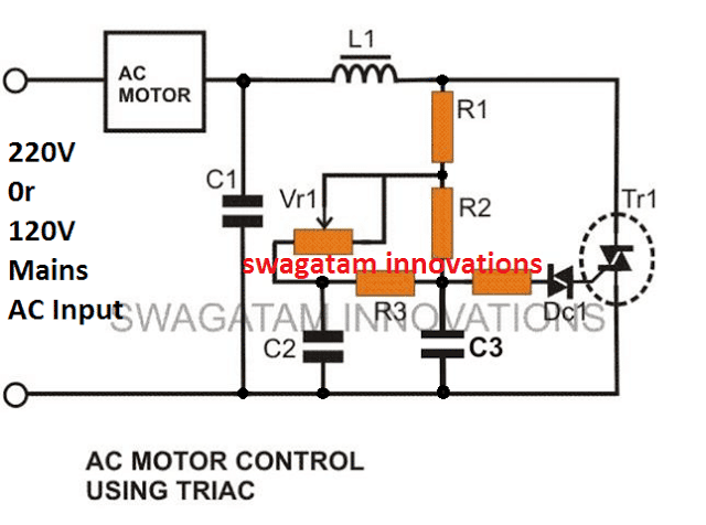
The parts list and the explanation is given in the following article:
https://www.homemade-circuits.com/how-to-make-simplest-triac-flasher/
If you want to use a full bridge network, you can consider using the following circuit:
" rel="ugc">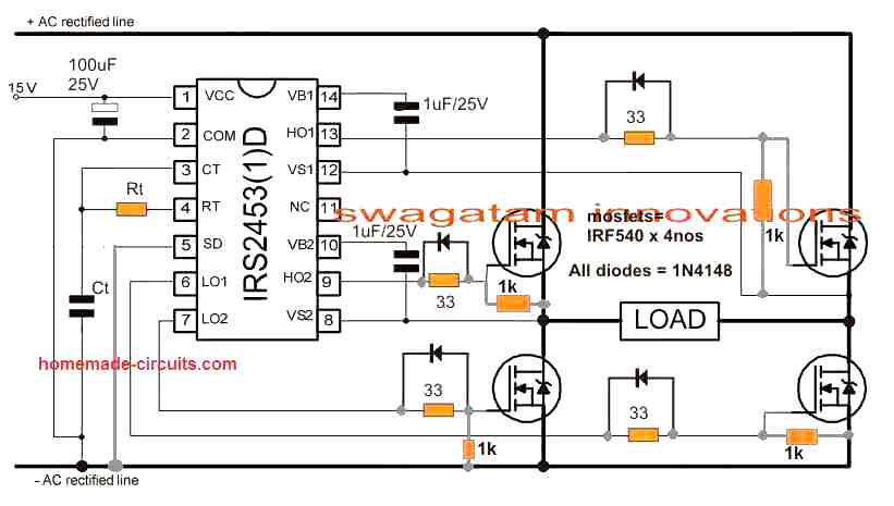
For the PWM control you can feed a chopping PWM to the gates of low side mosfets. I can show you how to do it, once you you build the basic inverter as shown above.
please can you explain the procedure of how transformer less inverter operate from the battery to it’s DC build up voltage ,component responsible and how they function in the circuit . Thank you
Transformerless inverter will require a DC input which should be equal to the required AC output or higher than the AC output.
Please what is the value of resistor at the bc547 transistor
you can use 10K.
Thank you sir, please what are the power rating of the resistor’s used in the 3kw inverter circuit
Hello Bernard, which figure are you referring to, I cannot see any 3kw inverter in the above article?
Sorry it was meant to be 5kw
Do you mean the second design?
Yes
All resistors are 1/4 watt 5% CFR
How will you get a standard AC waveform (e.g 50Hz) without using transformer in solar inverter ?
By suitably adjusting the values of R1, R2, C1
I am looking to build a reliable 34 vdc to 8-24vac inverter. It does not need sine wave and most 50 vac. It would seem that most of the circuits would work, but are overkill. Will they work at the lower voltage?
THANKS
You can try the following concept, and modify the arrangement to suit your needs:
" rel="ugc">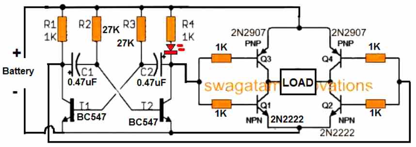
Thanks!
Is there an explanation page? I presume the frequency is 50 hz. Do you have a formula to calculate the frequency? What diode does it use? I presume the output voltage is .707 x the DC input voltage
The circuit using T1 and T2 is a transistor astable multivibrator circuit which generates alternate oscillating pulses feeding the bases of the Q1—Q4 bridge transistors.
You can find the frequency formula online by searching the phrase “transistor astable frequency formula”.
There’s no diode used in this circuit, except one red LED.
The output voltage to the load will be almost equal to the battery voltage or the supply input.
Sir I ran a simulation for the schematic for circuit with IRS2453 suggested by you but got some error. Will it be right to make this circuit practically?
Hello Arvind, Simulation softwares can be sometimes wrong, so the best way to test a circuit is by building it practically and then checking the results. You can first try the basic IRS2453 inverter circuit shown at the end of the post. Once you complete it successfully, next you can try upgrading it with a 555 PWM control.
Very good
Sir thanks to you for such website, which provides so much information to many people.
Sir I want to build 3000 watts 150 VDC to 220 vac pure sine wave inverter, so please help me. Please provide circuit diagram, all used components name and their values.
Thank you Arvind,
I think you should try the second concept from the above article, and see how it works for you. All the component numbers are given in the schematic itself. Let me know if you have any problems understanding them. But remember the design is recommended only for the experts in the field of electronics.
hi. what is the purpose of the diodes D1 and D2?
It is optional, it helps to provide perfect ON/OFF inputs to the mosfets
thanks..but still i would like to understand what the diodes are doing exactly? as i see, they will reduce voltage levels at mosfet gate by 0.7 V?
The 0.7V reduction will not affect the mosfet conduction. The diodes make sure that there’s perfect 0V OFF periods at the mosfet gates.
thanks..so am i correct in interpreting that this perfect 0V OFF period will minimize shoot through current? is that the purpose?
That is correct! That’s the basic purpose!
awesome, thanks a lot.
You are welcome!
I will like to try it on my own let see if it will work
Sir can you make a VFD, variable frequency drive, circuit diagram directly from dc to 3 phase variable frequency ac please
Hello Farhan, presently I cannot figure out the circuit, it looks difficult. If possible I will try to design it.
OK sir I will be very grateful to you ❤️
hi,
ON the schematic using IRS 2453 circuit, seen 2 rezistors without value on the 3 v Zener diode.
What value shoud the resistors be?
Hi, you can use 10K for those resistors.
Good day! Very informative, thanks!
With this inverter topology however, I suspect that it won’t have a proper line and neutral lines. Hence protection circuits like rcd rccb/rcbo won’t work. What would you say?
Thanks, yes there’s no neutral in these types of inverter circuits…. the Live, neutral alternately fluctuate across the two output wires of the transformer.
Hello,
I am planning on adding solar to my house in small steps. My background is a Bachelor of Electronics Engineering Technology Degree from Devry , 1977. I also have a life time of tinkering and repair of all kinds of mechanical and electrical things including home wiring.
I am hoping to go about it a bit different and wanted your opinion on the feasibility of what my plans are.
I am looking to avoid any long 24-12 volt runs by hooking up the input of a buck boost board to a 100 watt solar panel and then hook the output to an inexpensive car inverter in the 150 to 200 watt range. I then am putting a full wave bridge rectifier on the output of the inverter and getting pulsed DC at what I imagine will be 170 volts or so. The reason for all that is so I can add one solar panel at a time and combine their power outputs without worrying about trying to synchronize a variety of inverter outputs. The more panels I add the more DC power will be available on the joined bus.
The issue I am looking at with this is that I need to then find an inverter that will take that 170 volt DC and convert it to a pure sine wave AC output and give me something I can use on my home appliances. I already have a transfer panel I configured for use with a portable diesel generator and I thought I could use that to switch circuits over as I add more panels.
I also need to add batteries to the mix, and in the beginning I will need to run the batteries into inverters and then to a full wave bridge rectifier and join that with the output from the solar panels as well as having a charging circuit for the batteries, which may be as simple as a battery charger running off the pure sine wave inverter. Eventually I will have enough batteries to not need to run them through an inverter and just have a bank adding up to the 170 volts the solar panels are outputting.
Is this too Rube Goldberg? It looks like your transformerless inverter designs would be ideal for the pure sine wave inverter part of the system.
In case you have not guessed, I am retired and on a limited income so I have to pinch my pennies and not do too much at one time. I love the idea of going completely solar because I hate the lock in that the power company has on distribution costs and then charging me again for the supply. (I live in Ohio where the choice program means the distribution and supply have to be separate costs.)
Anyway, let me know what you think. Any questions will be answered if I can.
Hi, thanks for the detailed explanation and for sharing your feedback. You can try the IRS2453 based transformerless inverter for getting a pure sine wave output, however that design is quite complex. Therefore I would rather suggest the first or the second design using IC 4047. This will produce a square wave output but if you succeed with this project it can be easily upgraded into a sine wave inverter using a few IC 555 circuits.
Thanks!
Hello Swagtam
I have an application where I need to generate 220VAC 50/60Hz 1500W pure Sine wave from a 24VDC Battery source. I have severe weight/size constrains and therefore I cannot use an inverter with step-up transformer which will be very heavy. I wonder if you can help with a schematic diagram and parts list. I have the ability to deign the PCB and fabricate the heatsink required. I can also have the capability to provide force air through the heatsink fins for cooling. The application will be located at a remote unmanned location and therefore should be highly reliable. Any help on this will be most appreciated.
Simon
Hello Simon,
It is impossible to step up voltage or current without using a transformer, so i am sorry I do not have any other alternative options for you….
Hello Swagtam
Thank you for your response. So sorry that I was not explaining myself. My idea was to generate the Bridge excitation High voltage using an Isolated 24VDC to 315VDC 1500W converter. This way there is no need for the heavy, large Step up 1500W transformer to step up the low 50/60Hz ACV to 220VAC. So I thought, maybe you have a schematic for this solution. Probably I will need also a low pass filter for converting the modified sine-wave to pure sine-wave.
Sorry for the confusion
Simon
No problem Simon,
Yes I understand the question now, however presently I do not have this schematic with me. I guess there has to some sort of storing device for raising the voltage and current. If an inductor is not used then probably a capacitor would be required for the stepping up function, and capacitors can be bulky too. The best option could be a ferrite transformer.
hey is it possible to convert 5v dc to 50-80ac , my idea is to boost the 5v to 70v dc(peak to peak voltage) then pass it through the MOSFETs to get 50V AC
It is possible, you will need a transformer with a 5V primary and 80V secondary winding.
Alright but though I can’t find such a transformer online ????
Yes it is a made to order transformer
Good morning sir.
I have concerns with the inverter using the IRS2453 (1) D circuit. I did the research on the irf540 mosfet the Vds voltage is 100V and the ac voltage can be how much? Thank you
Hello Daoud, you are right, IRF540 was mistakenly mentioned in the diagram. I have corrected the diagram now with IRF840 devices. Thank you for pointing it out.
Hi Mr. Swag. Thks alot for ur wonderful innovations and assistance. Am impressed.
Pls i need a 2kva, 2.5kva, 3kva – 5kva generator avr circuits particularlly for elepaq gen sets
Thanks Vincent, I do not have those circuits right now, I may try to find and update it soon
Hi Swag,
Sorry this does not have anything to do with the above but just to find out if you are keeping well. You have been very quiet.Are on Lockdown in your country.
Thanks Bernard, I am fine so far, there is lockdown in our country but I am always available in this blog answering to comments, so whenever required you can feel free to ask questions here, I will be most happy to help!
I’m curious about the output impedance (load invariance/ability to reject noise from poor power factor loads) of high frequency inverters vs the conventional low frequency inverters.
One of the problems I noticed while running on generator power was that poor power factor switching power supply devices pollute the power, causing harmonic distortion to become excessive on the branch circuits connected to that genset. Inverters probably have a similar problem. I wonder if HF inverters are better than LF inverters in this respect?
I am not sure about the output impedance, but the power factor and the harmonics can be eliminated by adding a properly calculated LC network at the output of the inverter.
Hi Swagatam.
What frequency does the modulation of the 3kVA inverter need to run at if the reference triangle is running at 60Hz?
What are the key parameters of the MOSFET for the inverter if I am running a 400V DC bus?
Thank you for your fast responses.
Hi Luke,
the slow triangle wave must be at 60 Hz, and the fast triangle waves must be at any high rate depending on how many pillars or blocks are intended on each cycle of the SPWM waveform.
Ideally the VDS of the mosfet must be 1.2 times the 400V rating, and current rating ID should be 1.5 times the maximum load current
Thank you Swagatam. Very Helpful. Do you have a link to a sample feedback circuit by chance? I think I saw one of your articles where you fed back the rectified voltage to the 555 timer at the RC pin?
Hi Luke, yes that’s correct….you can try the second circuit from the following article:
https://www.homemade-circuits.com/load-independentoutput-corrected/
It can be configured with any MOSFET stage for controlling the output voltage of the inverter
Hi Swagatam
With a 400VDC input voltage and transformerless pure sine full bridge inverter, can I control the modulation triangle wave to get either 220VAC out or 120VAC out? Do I control the amplitude or the frequency?
Appreciate all your responses.
Hi Luke, yes you can use a chopper circuit with PWM to reduce the voltage to lower level, and also apply a feedback circuit to control the peak level of the voltage.In fact the feedback circuit alone should be enough to reduce the voltage to any desired levels. Yes the amplitude will be controlled by the feedback…
For the transformer less pure sine inverter above with IRS2453 chip, what efficiency can you get out of it at 3000W and 220VAC output? OR, what efficiency did you get with the circuit shown with IRS2453.
Very cool website by the way.
Thanks
-Luke
Thank you for liking my website, as per the design it should be over 95% if the DC input is from a solar panel or windmill..I have not tested the efficiency practically…
Referring to the inverter circuit using the IRS2453 design and it being a transformerless type:
A curious question for those adding a center tap and that because here in the states some appliances require not only 220-240vac but the neutral leg as well….
Would there be any problems with center tapping the DC and using that as the neutral if that were possible (i.e. physically speaking or stacking matched capacitors in series )? Also, if say this inverter were of significant power (say 3-7kw) wouldn’t that be the most economical way of achieving a 120-240Vac output? Thanks.
That won’t be a problem at all, and should work exactly as assumed by you!
I appreciate you having patience and your kind reply. After considerable web searching and hitting brick wall after brick wall I’ve been trying to find the most economical way of building an inverter that can be used as an emergency backup for my ‘prone to lose power home’ & living out in the country. I’m also considering building several smaller ones with the hopes of working harmoniously; while thinking ‘have one lose everything’, ‘have several lose a little’. Notwithstanding, having more determination perhaps than resources (and possibly good sense) and entering back into electronics after an absence in time —-I find your website very refreshing and appreciate your time & help.
Regarding my initial post: Not really wanting to assume anything I’ve considered your reply and my thoughts about using the DC Supply center point as a neutral. Is your concern centered on “an elevated ground perspective”, an “unstable floating ground” or something more complex?
Thanks again.
Which DC side exactly are you referring to? I thought you are referring to a transformer as the load, and use the transformer output AC side with a center tap for dividing the AC to 0-120-240V
Sorry for the confusion. I was intending on building a transformer less inverter. While doing so I was hoping to use the DC supply of course as power supply for the rail to rail 220-240 AC source and the same DC’ source ‘midpoint potential’ as the “neutral”. In doing so, I’d create a 120Vac output from that “neutral point” and either of the lInes out. If that’s doable, then I wouldn’t need an expensive transformer to produce both 230-240 & 120vac, not to mention a wire being cheaper. Does this make any sense now? Thanks.
OK, understood, but sorry no, I don’t think the DC side could be divided into two to get the neutral….because the AC output is will be conducting across the left/right MOSFETs arms, with respect to the ground line, I cant figure how the mid-point of the DC will respond to this conduction
[email protected]
Sir pardon me for interrupting, but there is a very elegant solution for powering the low voltage electronics from any voltage between 100v to 250 voltage Dc and probably more if you search a bit. All you do is to locate any off the shelf SMPS units 12 or 15 as d2esired in any amperage from .5A to 2A as per your requirements which should be more than adequate for dropping high DC voltage for powering these kind of circuits. All yo9u got to do is connect the DC in directly to the Ac voltage in. Only very rarely you will get a single Diode in such Smps, even in these cases you just reverse the input polarity and the unit will function properly. This is a more elegant and a simple non heating approach to these applications.
Sorry, Prashanth, I don’t think I understood your idea correctly? Please explain what is the primary objective of your circuit, and how should it be implemented?
Hello dear sir,
this is very informative & helpfull. Sir i have 30 solar pannels. Each pannel has 60vdc and 60watt (1A). i connected 5 pannels in series. These have 300vdc 1A.
Because i have 30 solar pannels i have 6 array of 300vdc & 6 Amp. Please suggest a suitable circut for me according to my solar pannels. Before i am using a circut but i am not saticfied.
Thanks Abubakar,
you can try the following simple H-bridge design with your 300 V DC input
For the oscillator, you can try implementing the following design,
Hello Swag happy new month, Sir i finished building the 3kva with all the components, my major problem now, is the frequency and the PWM
I am having 4KHz at the AC output frequency and the voltage is dropping at every load apply to it. Sir please I really need your help now.
Hello Moses, please check the inverter without the IC 555 pwm integration. Ans please provide all the details regarding the input voltage, current, low side mosfet gate average DC with pwm without pwm, load capacity etc
Sir, would like a circuit that involves only N channel mosfets .Also let me Know if the 4 mosfets can makeba 5000w inverter and run the load at it’s maximum. If they cannot hold 4
5000w max,how do you add mosfets on a h bridge system?
Evans, for N channel you can try the following link
https://www.homemade-circuits.com/simplest-full-bridge-inverter-circuit/
you ca use IRF3205 for getting 5kva
hello sir, how many irf3205 mosfet to be used and can I make use of IRFB4137PBF to build the 3-5 kva transformer inverter
Aanu, you can use 4 MOSFETs on each channel
Hi,
There are two resistor without values. The ones connected to the bases of the leftmost b547s.
Please what are their values?
Hi, you can use 1K for those resistors…
Hello Sir, I guess you didn’t get the message i sent to you last week, that I was able to finish the full bridge square design and I have optimal result for the load, I tested it with 25w bulb 60w bulb plus 100w bulb and there is no hot IC or fet but my problem now is that I notice a voltage drop when load is being applied to it and I apply the PWM stage for output voltage regulator, the ic 2453 started heating when load is connected to it but once I remove the ic 555 and the BJT transistors still connected to it, It work fine without heating of the ic2453. So please engr I need your help in this regard, how do I solve this problem. Thank you
Moses, connect the 12V supply with the ICs Vcc through a 100 ohm resistor, and connect a 100uF capacitor across the Vcc and ground pins of the IC. Also connect a diode across the Vcc and ground of the IC with cathode of the diode towards the Vcc. THis might help to correct the heating issue of the IC
Irs2453D. Ct. Rt kya hai
capacitor and resistor for setting output frequency
Hello Sir,
I have removed the PWM ic 555 and Op amp ic as you instructed me and I got optimal result for the load, and I live it to work for like an hour to see if there will be any heating of the fet or the ic, but no heat and i started by applying a 25watts bulb, the ic irs2453 instantly started heating and got burnt, I try again and it burn second time. Sir please guide me, I need your help thanks.
Hello Moses,
Full bridge circuit using 4 n channel is always difficult to optimize since it involves a complex circuitry around the MOSFETs. You can try the following design which is a tested one:
" rel="ugc">
It uses two half bridge instead of full bridge IC but the MOSFET configuration is the same…here 22uF is used for the capacitor, so you can also try using 22uF and check the difference. Connect a 40 watt bulb in series with the drain of the MOSFeTs for safety
Hi Eng Swag I finished building the 3kva, but I have a problem (1 I apply 310vdc and I am having 160vac output if I test it with multimeter, but if I use analog meter it wouldn’t move.
And you mentioned reverse diode, where do I fix it. please sir help me
Moses, you must first build the basic full bridge square design without the PWM, and get optimal results for the load. Next, you must check the PWM IC 555/op amp response separately on an oscilloscope, and once confirmed you can go for the final integration and the results.
Please sir I am Moses, the 1uF/25V in the diagram, is it electrolyte or ceramic capacitor
non polar strictly.
Good day Engr., pls I did not know why all the circuit that I ve been downloaded here about transformer less inverter didn’t work I just tried another one now again it did not work pls sir I need your help very seriously I have my batteries bank of 230v DC pls help me.
Good day John, all the concepts presented here are perfect and drawn as per the datasheets, by the way these are not for the newcomers. It is for the advanced users who know all the basics of inverters and know how to troubleshoot.
No complex circuit can work unless it’s built stage wise and confirmed stage wise, and with proper understanding.
If you think it will start working just by joining the parts, then I am sorry it will never work in that way.
You must first try the basic full bridge inverter using the shown IC IRS2453. Once you confirm the working then we can proceed ahead.
By the way which one have you tried so far, and how did you test the various stages? Please describe it, I’ll solve it for you!
good morning Sir…engineer please help me with 12v battery automatic charger circuit diagram, i want to use 15v transformer.. when the battery is 9v it start charging and stop charging when is fully charged… thanks
Sunshine, there are plenty of 12V automatic charger circuits in this website, you can easily find them through the search box.
Sir, thanks for the update. but I need a special tutorials on inverter and its operations because I’m an Electronics student.
i connect IRFP260N MOSFET
i complete this circuit and it worked, thank you sir
Glad it worked indranil, congrats!
sir I complete transformer less circuit but 1 problem here 2SK 4124 MOSFET is not in my local area
can i used any igbt for this circuit
Indranil, if your supply input is 310V DC then you can select any 500V mosfet or IGBT, but I would recommend to go with mosfet first. And remember there are 3 stages involved here, so make sure to build and test them separately using an oscilloscope before integrating them together.
Thank you sir
You are welcome!
Thanks for your reply, you will hear from me.
Can i used ct= 1000uf and rt = 100k
1000uF is too large it may not be correct for getting 50Hz or 100Hz, it would be better if you could test it with some practical and error.
OK
Can i used this circuit in ac water pump please guide me
yes you can!
Hello!dear swag sir I complete 3 kva transformer less circuit but facing two problems 1st,ic 2354d over heating 12 &15 volt both tried 2ndly there is 150 volt out put how to phase split for getting 220 volt out put input is 230 v DC Rt is 470 ohm CT is 100 nf 104 please guide me
Thanks
Hello Gulab, I am glad you could finish the project.
If your ICs are getting hot, make sure you are using 12V for the Vcc of the ICs, and make sure you have reverse diodes connected across the mosfets.
The output voltage will depend on how the transformer is selected in accordance with the PWM RMS. For more info you can read the following post:
https://www.homemade-circuits.com/inverter-voltage-drop-issue-how-to-solve/
Hello, yes I completed as per schematic of 5 kva ,but supply 220 v dc through solar panels , in result of giving 240 v DC from s.panels I got 160 v ac and secondly ic 2353 d getting hot .
what is the voltage across the Vcc and ground? make sure it is not more than 15V or 12V preferably, also connect a 1000uF capacitor across these pins.
Hello dear swag sir,I checked completely before questioning to you ,all as per scheematic but still I’m facing there’s two problems first ic become hot mybe this happens and secondly out but is 150 v ac while I m giving 240 vdc directly from s,panels ,because I’m trying to make ac220 directly from s,panels through ur circuit ,please guide me how I can get result of 220 v ac
Thanks
Hello Gulab,
Could you tell me how did you convert the panel voltage to 15V for the IC?
For getting 220V from SPWM based circuit you must provide a 310V DC input to the mosfet bridge. A 220V input will only result in producing around 150V
sir, I used 10 k 10 watt resistance and 15 v 2watt zener for ic now I got ur answer for 220 v ac I must give 310 v in input as u answered Thank to u I later try then tell u
OK no problem!
Hello swag ,sir I want to replace sg3525 against irs2453d can I ,is it is possible
Hello Gulab, sorry that may not be possible, because irs2453d is a full bridge driver while the SG3525 is a push-pull driver
sir,very kindly thankfull to you for Guidance
Hi,
I built the 3KVA transformerless inverter. initially I had problem that the IRS2453D would not oscillate, Once i grounded the pin no.5 it started oscillating. Now My problem is I am getting a square wave output and not sine wave as needed. What suggestion can you give. For the supply to Ic’s I have used a small 12 V 1 amp SMPS whose primary I connected to 160V D.C. input as its a universal input it works fine. your comment on this?
Yes, pin#5 which is the shut down pin needs to be grounded, I’ll correct the diagram soon.
For getting sinewave PWM you must implement everything that has been shown in the diagram, right from the opamp, IC 555 stages to the low side BJT connections….you will have do it stage wise by checking and verifying each of the stages separately.
sir my inverter ic is sg3525 can i join the pin6 (RT) of the sg3525 to pin3 of ic741,and join the output of lm555 with pin2 of ic741 while the output of ic741 goes to the bjt/fets to turn it to pure sinewave inverter
abioye, you will have to show a schematic to enable me to quickly understand it….if possible draw a schematic and send it my email address…
Hello Mr Swagatam,
I would need to extend the circuit to a suitable MPPT optimizer.
Hello Lubos, that will make the design much complicated and huge.
We need to design a 1KVA transformerless inverter can we know the specifications of the circuit
the specifications solely depend on the mosfet rating, and the input supply rating, and these can be tweaked as per user preference.
The IC basically works with 12V DC
Just as the original requester mentioned, Prius’s are still being manufactured but the 200 VDC 120VAC inverter isn’t. I’m a computer geek and photographer, with no experience or expertise in building these types of devices. Is there anyone out there who would be willing to build this for $100 to $300+/- and I’m probably not the only one who would be willing to pay to get this. 🙂 Thanks for any help.
Thanks for your interesting feedback Davis, I hope somebody will read this and respond to fulfill your request.
Hi interesting article , Is any one out there interested in developing a 4 kw single phase with high dc voltage input .. 800 vdc . must be off grid My company requires 6000 next year as well as 1000 3 phase units same input
over the next 4-5 yrs we will need some 200,000 units
please contact me directly on my email [email protected]
Hi, Thanks for the offer, I have sent you an email to learn more about the specification.
Sir,
Actually, I am designing 3 kva transformerless inverter as per your circuit and there are 160v DC input and 230v output. Now there are 15v DC supply is required to operate 555, 741 and IRS2453 ics. Now my question is that how can I providing 15v DC to that ics from 160v DC input.
Prashant, you will have to do it as suggested in my previous “48V inverter” link…use MJE13005 for the BC546, for the resistor use 10K 5watt, and 12V zener for the zener, and instead of 48V you will supply it with 160V and obtain 12V across the emitter side….measure it with a load connected
Can I directly connect 6RI100E-080 rectifier to 230v AC supply for generating DC supply?
yes you can, but make sure the load current is much less than the rectifier current rating, or vice versa….
There are some questions related 3 kva inverter.
1. At full load, only 4 mosfet enough or required more!
2. 741 op amp required negative voltage, so how can generate it?
3. DC voltage is 160v and 555 & 741 required 15v. So how can generate it?
4. What is the values of 10k preset pot set?
5. In circuit diagram, mje13005 indicated. So what is the use of it in this circuit?
1) The total current of the mosfet on each channel must be higher than the output max current, this you will have to verify from the datasheet, by the way I have already provided the mosfet details in the article.
2) IC 741 will not require a dual supply, just make sure that the leakage or the offset voltage from pin#6 is appropriately blocked, the attached 3V zener should be hopefully able to do it.
3) 12V for the ICs can be achieved using an emitter follower design, as depicted in the following 48V inverter circuit:
https://www.homemade-circuits.com/48-v-inverter-circuit/
for 160V replace the 10k with 100K, and replace the BC546 with a TIP122, the zener can be a 12V zener
4) 10K presets are normal presets, use good quality ones, multiturn type.
5) MJE13005 is a mistakenly shown, please ignore it.
My dear Sir,
In 48v dc ckt, how can I apply 220v AC at transformer side without AC supply?
sorry, I did not understand what you are referring to?
220V is the output from the transformer…48V is the DC from battery, I hope you have understood now!
Dear Swagatam sir,
I regularly watch , try to learn and enjoy your informative site.
I would like to do a 50v dc in 600w inverter , using mosfet full bridge and transfo with out center tap.
I plan to use 2 nos LM5109, half bridge gate driver and 4 Nos mosfet STP80100., and a transformer.
Regarding LM5109, half bridge gate driver, i need to know about the input to be provided at pin 2 and 3. Request you to give me this information.
Thank you dear Musthafa,
you can use any standard IC 4047 oscillator circuit and use its two outputs to feed pin#2/3 of the your half bridge driver IC…but remember the second bridge IC should be fed with an anti-phase signals from the IC 4047…this may be done by using NPN BJT stages or by using NOT gates.
So kind of you sir.
I have used one of your ckt,Pure Sine Wave Inverter Circuit Using IC 4047, feeding the 4047 otputs to the LM5019 Full bridge half bridge gate drive,Q to left top, Q Not to right top, q to right low and q Not to left low.
In this arrangement, how can I add voltage feedback control for getting a stable output?
You can add the following concept with the low side mosfet gates for getting a constant output
https://www.homemade-circuits.com/automatic-output-voltage-regulator/
but make sure to do it with proper understanding.
By the way which 4047 circuit did you use??
Dear sir,
Thank you very much for your kind and quick reply
.I have emailed to [email protected] , the schematic that I plan to use, utilising your 4070 (by mistake mentioned it as 4047) oscillator circuit, with 555 ic generated pwm for sinewave, as input to the LM5109, x 2 nos gate drivers for controlling a full bridge mosfet inverter.; also output voltage regulation schematic.
Kindly correct me the mistakes, in the attatched circuit that I have concluded.
I will be thankfull, and appreciate, if you could post the circuit after refinement, in your website.
Dear Musthafa, the wiring is correct except the following:
use 1K resistors for the low side mosfets, otherwise the voltage regulator circuit will short circuit the IC outputs directly.
In parallel with the 1K resistors put 1n4148 diodes, cathode towards the IC and anode towards the gate
and I hope you would be using only the 4047 stage and exclude the lower PWM stage because it is not required.
by the way you have used a 4047 circuit and not 555/4017 circuit in your diagram, which is correct and the recommended design
rest all looks fine.
Hi Swagatam,
im wondering is there any refferences diagram to make andj V and A ps using dc input around 50v, its unknown amperage, so i wish to have it (PS) as the maximum as possible V and A from the source. i cant find transistor LM317HV or K D718 on local electronic store, i only have IRF 540 and 530, also 555.
Hi Tubagus, you can try the following concept
https://www.homemade-circuits.com/100-amp-variable-voltage-power-supply/
Hi Swagatam,
Thanks for the post! So I am not able to meet the circuit requirement that the fed input DC supply must be equal to the required output peak voltage level. So if I’m interested in using a transformer design instead, can you point me to one of your former projects that I can study? As another option, I’m wondering if using some Vicor V300A48C500B modules to convert the 200 VDC to 48 VDC would be easier (though perhaps more expensive) and then running the 48 VDC into an off-the-shelf 48 VDC (solar?) inverter. Thanks for the help!
Thanks Ralph,
You mentioned 200VDC, you can use this DC for operating the above inverter circuit. 200V may be slightly higher than the the required 160V specs, however it can be adjusted by suitably adjusting the PWM pots associated with the IC 555. By the way could you specify the source of this 200V DC, will it be from the batteries?
If you think a readymade option would be better, you can go ahead with it as that would save you from making this complex design and all the hard work. 200V to 48V converter would be fine but it could cause some unnecessary power dissipation, and waste precious watts in the process.
I have stayed up all night learning these inverters to where is was ready to nuts, most of these parts I don’t have and spending money on all this stuff is not why I am building one. That’s why I asked about the ges002. It’s cheap and everything I need in small plug in board. If had more time and money I would built one of your circuits in heart beat.
I think the finishing and the assembly quality of the product indicate how well they may work. A nicely designed and assembled commercial product will mostly be a good performing product.