Our power amplifier only uses a handful of widely available and inexpensive components. Despite this, it can deliver an effective power output of 50 W into an 8 ohm load or 75 W into a 4 ohm load.
If distortion is below 0.3% at these maximum power levels, it drops to less than 0.01% from 20 Hz to 20 kHz for any output power between 1 and 20 W, which is the most common range of use for this type of device in a domestic environment.
It should be noted that these characteristics were not obtained through theoretical calculations, but rather through measurements taken in real-world situations on prototypes made by the author.
Moreover, all audiophiles will tell you that the sound of MOS power transistors is smoother, warmer, and above all less aggressive than that of bipolar transistors.
It comes close to the sound, judged so inimitable, of tube amplifiers. This appreciation is much more subjective than our numerical characteristics, so we invite you to form your own opinion by taking your soldering iron without delay.
An original circuit
The most difficult part of a 75 watt power amplifier is not, as is often thought, at the level of the power transistors themselves, but rather at the level of their control.
In bipolar transistor amplifiers, it is necessary to provide sufficient current to the power transistor base so that they can function properly.
In a power MOS-based amplifier, on the other hand, it is necessary to provide a sufficient voltage to the gate of these transistors to drive them correctly.
And it is precisely the supply of this voltage that often poses a problem, given its value and its necessary referencing with respect to the supply voltage.
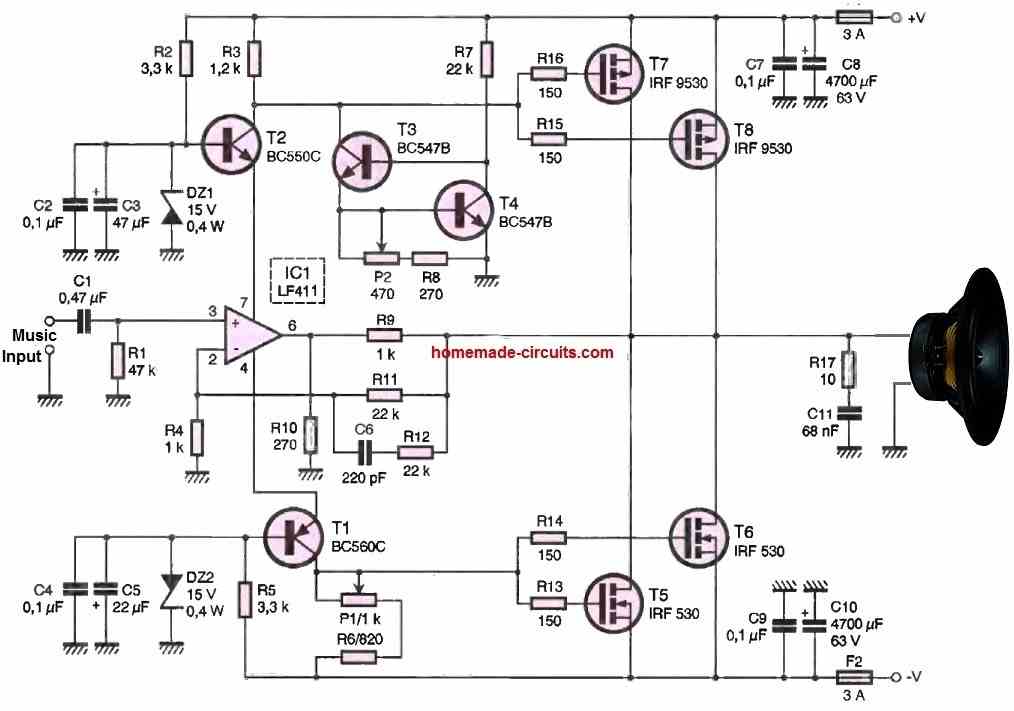
As you can see from the examination of Figure 1 below, the 75 watt power amplifier circuit used here elegantly and originally solves this problem, even if this originality is over twenty years old, since we first saw it applied in a Texas Instruments application note from the 1980s (with bipolar transistors).

For the moment, let us forget about the transistor pair T3, T4 and focus on the rest of the circuit.
The operational amplifier IC is configured as a non-inverting amplifier but, instead of using its output voltage to drive the power transistors, a voltage that would be insufficient in this case, this voltage is sent to ground via resistor R10.
As a result, the current consumed by the amplifier on its power supplies is a function of the voltage seen at its input.
This current, precisely, flows through resistor R3, on the one hand, and resistor R6 in series with potentiometer P1 on the other.
It creates in these resistors, according to Ohm's law, a voltage drop that is proportional to its value and, therefore, to the input voltage IC1.
It is this voltage drop, referenced with respect to the supply voltage, that can then drive the power MOS transistors T7, T8 on the one hand, and T5, T6 on the other, under excellent conditions.
Due to the use of complementary transistors, a common-source configuration can be used for this power stage, which facilitates its implementation.
As the operational amplifier IC1 cannot support the power stage's required ±30V power supply voltage, its power supply is stabilized at 14V by means of transistors T1 and T2 and zener diodes DZ1 and DZ2.
Note that this stabilization does not call into question the previous explanation since we only considered the current consumed by amplifier IC1. Let us now examine the role of T3 and T4.
You probably know that in any power amplifier of this type, theoretically operating in class B (but practically in class AB), the power transistors conduct alternately for the positive and negative alternations of the signal to be reproduced.
Unfortunately, even if they are perfectly complementary, the transition from one's conduction to the other when the signal is close to zero and changes polarity never occurs perfectly and generates what is called crossover distortion or connection distortion.
This distortion is all the more annoying as it occurs at low output power, i.e., where the amplifier is most often used.
To avoid this, the power transistors are kept weakly conducting at all times, and this weak conduction is characterized by what is called the amplifier's quiescent current. It is also because of this permanent weak conduction that these amplifiers are not called class B but class AB.
Our 75 watt amplifier circuit is no exception to this rule, and this low quiescent current is determined by the T3-T4 pair set up as a constant current generator (or absorber, if you prefer).
Depending on the position of potentiometer P2, the current absorbed by T3 is more or less significant, thus increasing the voltage drop across R3, which makes T7 and T6 more or less conductive.
Due to the symmetrical properties of amplifier IC1, this increase in current in R3 is reflected by the same increase in R6-P1, and the circuit remains balanced.
To prevent any thermal runaway of this quiescent current, transistor T4 is placed in contact with the heatsink of the power transistors.
When it heats up, this reduces the base/emitter voltage of T4 and thus the current absorbed by T3, thereby achieving temperature stabilization of the quiescent current.
The network R17, C11, on the other hand, is called a Boucherot network on this side of the Atlantic and the Channel and a Zobel network elsewhere, stabilizing the amplifier by limiting its high-frequency response.
Construction
The implementation of our 75 watt amplifier presents no difficulty. The components used are available everywhere.
However, if you have difficulty finding the power MOSFETs, they are in stock at SELECTRONIC, as well as C8 and C9 (at the right size and pitch!), and the "comb" heatsink is used.
The shape and size of the latter are not essential, except that they facilitate the mechanical assembly of power transistors.
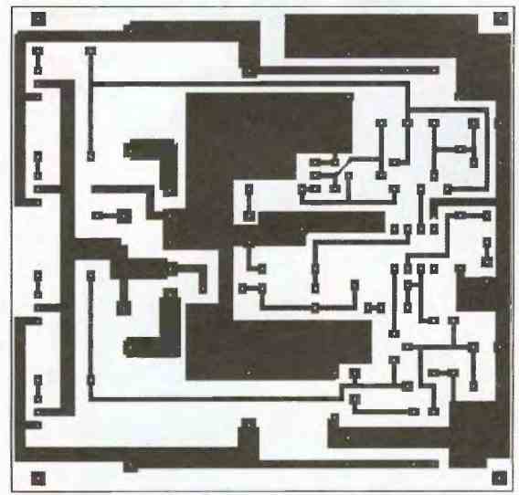
The printed circuit board is shown in Figure 2, and to maintain the amplifier's excellent performance and unconditional stability, we advise you not to modify it and, above all, not to reduce the width of the tracks or the size of the ground planes.

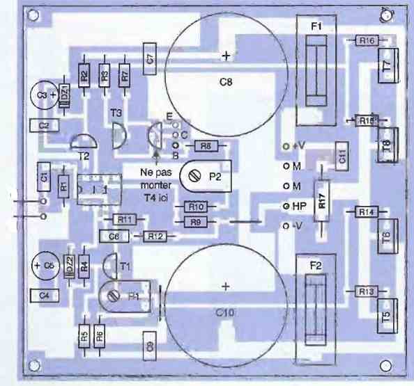
The component layout should be done following the indications in Figure 3.

Proceed in the usual order: integrated circuit socket, resistors, capacitors, diodes, and finally transistors.
Regarding the latter, note that although its location has been provided on C1, T4 should not be soldered there.
This transistor must be placed in direct contact with the power transistor heatsink and connected to the three corresponding points E, B, and C corresponding to its emitter, base, and collector, visible on the printed circuit board.
As for us, and as you can see on the model, we simply glued it (with fast epoxy glue) to the heatsink, between the central power transistors.
These will be mounted with their entire leg length, which will facilitate their application to the associated heatsink.
A "comb" type heatsink, like the one we used, is obviously the most practical for this type of implementation because the amplifier's printed circuit board can be fixed to it using two brackets at the same time.
The power transistors will be screwed onto this heatsink after interposing the classic insulating accessories in mica or Kerathemn and using shoulder washers.
Regarding this, note that the simplest method for attaching components to a heatsink of this type is to use so-called "Taptite" screws, available.
These screws do not require a nut and make their own threading into the heatsink during their first screwing.
They can then be screwed and unscrewed without any problem like normal screws in a traditional thread, which is very convenient.
Once your transistors are fixed on the heatsink, do not forget to verify the perfect insulation of their metal tab with respect to it. A drilling burr or a crimping of a shoulder washer can quickly cause a problem.
How to Use and Set
The power supply for our 75 watt power amplifier circuit is not shown here because it consists of a transformer followed by a rectifier bridge whose power is proportional to the number of amplifiers to be operated and the output impedance used.
Note that this power supply is not equipped with filtering capacitors since they are located on the amplifier itself in the form of C9 and C10.
The ideal power supply voltage at full load, to obtain the maximum output power, is ±30V.
Therefore, a good transformer with a 24V secondary is suitable because this will provide about ±35V with no load and about ±30V with maximum load.
For each amplifier supplied and for an 8-ohm load, the transformer power should be at least 72VA (3A at 24V). The rectifier bridge should obviously also be a 3A model.
For a stereo implementation, these values should be doubled, which gives 144VA (150VA in practice) for the transformer and 6A for the bridge.
For operation under 4 ohms, the consumed current is obviously higher, and the transformer should be a 120VA model per amplifier, while the bridge should be a 5A model. These values should also be doubled for a stereo implementation.
Before using this amplifier, it is necessary to adjust the potentiometers P1 and P2. To do this, set P1 to the midpoint and P2 to the side of its maximum resistance.
Replace the fuse F1 with a milliammeter and power on the circuit.
Then, adjust P2 carefully to read a current of about 50mA. Leave the circuit powered on for a good half-hour and check that this current has not drifted by more than 10%.
Be aware that if T4 has not been brought into contact with the power transistor heat sink, as explained above, this current may drift significantly and even lead to the destruction of the power transistors due to excessive heating.
Otherwise, as you will be able to verify, the stabilization obtained is excellent. After an hour of testing our model with 20W effective permanent output to the load, the idle current returned to its cold value within a second after the signal disappeared.
If you want to fine-tune your settings, then place a DC voltmeter at the output, short the input to ground, and adjust P1 to minimize the DC output voltage.
However, a value of 50 to 80mV is still perfectly normal. Warning! This adjustment affects the idle current and requires P2 to be adjusted accordingly.
When done, you can replace F1 and enjoy the excellent qualities of this amplifier.
However, it should be noted that distortion rates as low as 0.01%, which are intrinsic to this amplifier as long as the output power remains reasonable, can quickly be spoiled by poor grounding or by noise and hum induced by the preamplifier that precedes it.
Total distortion measurement indeed involves the concept of noise, and it is not enough to have an excellent power amplifier to automatically benefit from the lowest distortion.
Another Simple 75 Watt Power Amplifier Circuit

Circuit Component Value Calculations
Introduction: The process of calculating values for various circuit components involves a balance between criticality and simplicity.
This section outlines the rationale behind selecting values for key components within the circuit.
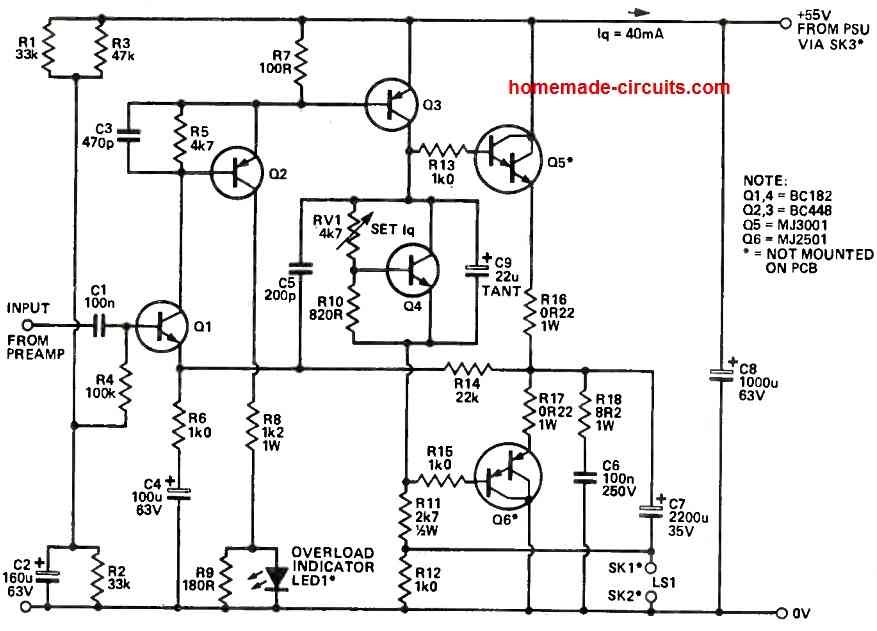
Baseline Potential Establishment: The values for components R1, R2, and R3 are primarily chosen to establish a baseline potential at Q1.
This strategic selection ensures that capacitor C7's upper end reaches half of the supply voltage, while also accounting for voltage drops across R4 and R14.
Preventing Loudspeaker-Related Issues: The inclusion of R12 serves the purpose of allowing capacitor C7 to charge or discharge when the loudspeaker is disconnected.
This preventive measure avoids abrupt noises that might occur if the loudspeaker connection is established after switching on the amplifier.
Additionally, it ensures the amplifier's functionality even in the absence of the loudspeaker load.
Enhancing Q3's Performance: The value of R11 is determined to facilitate a substantial DC current through Q3.
This current exceeds the anticipated 2mA peak base currents required by Q5 and Q6 during peak output demands.
The chosen value ensures Q3's collector current is around 10mA, a level that prevents significant variations in voltage at Q3's collector due to the charging and discharging of high-frequency compensation capacitor C5.
This stability contributes to achieving high sound quality.
Transistor Considerations: The transistor chosen for Q3 must be capable of withstanding a collector-emitter potential of approximately 80V and possessing a permissible power dissipation exceeding 550mW.
Beyond these specifications, the specific transistor type chosen is less critical to the circuit's performance.
Current Regulation and LED Activation: Components R8 and R9 are designated to regulate current levels in specific scenarios.
Under normal operating conditions, where a collector current of 5-6mA flows through Q2, the LED remains unlit due to the modest current level.
This situation results in a roughly 1V drop across R9.
Clipping and LED Illumination: In instances of amplifier clipping, Q2 progressively supplies increased drive current to Q3. This leads to a rapid rise in the voltage drop across R9, causing the LED to illuminate.
The presence of R8 limits the peak current flow to 40mA, preventing excessive dissipation within Q2.
THD and Harmonic Distortion: At maximum output, the amplifier's total harmonic distortion (THD) at 1 kHz is approximately 0.1%.
The dominant form of distortion is second harmonic, which diminishes notably as output levels fall below peak power.
Undesirable crossover residues such as the 7th, 9th, and 11th harmonics remain below 0.01% in total, indicating their negligible impact on the overall output quality.
disculpen la pregunta , por que no se le realizan protectores de corto circuito de parlantes a los amplificadores anunciados , esto puede traer acarreado que se destruya la parte de potencia .
To protect the speaker you can use the following concepts:
https://www.homemade-circuits.com/loudspeaker-thump-sound-eliminator-circuit/