The circuits I have explained here are 10 best small timer circuits using the versatile chip IC 555, which generates predetermined time intervals in response to momentary input triggers.
The time intervals can be used for keeping a relay controlled load ON or activated for the desired amount of time and an automatic switch OFF once the delay period has elapsed. The time interval can be set by selecting appropriate values for an external resistor, capacitor network.
IC 555 Internal Circuitry
The image shown below represents the internal schematic of a standard IC 555. We can see that it us made up of 21 transistors, 4 diodes, and 15 resistors.
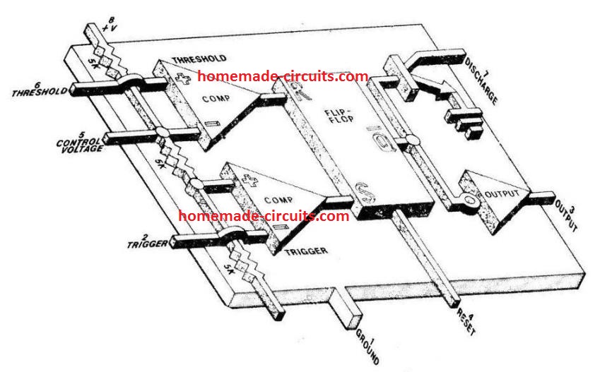
The stage involving the three 5 kohm resistors work like a voltage divider stage which produces 1/3rd voltage level at the non-inverting input of the trigger comparator op amp and a 2/3 voltage division on the inverting input of the threshold comparator op amp.
With these trigger inputs the two op amps control the R/S (reset/set) flip flop stage, which further control the ON/OFF conditions of the complementary output stage and the driver transistor Q6
The output state of the flip flop can be also set by triggering the reset pin 4 of the IC.
How IC 555 Timers Work
When IC 555 is configured in the monostable timer mode, the TRIGGER pin 2 is held at the supply level potential through an external resistor RT.
In this situation, Q6 remains saturated, which keeps the external timing capacitor CD shorted to ground, causing the OUTPUT pin 3 is to be at a low logic or 0 V level.
The standard Timer action of the IC 555 is initiated by introducing a 0 V trigger pulse at pin 2. This 0V pulse being below the 1/3rd level of the DC supply voltage or the Vcc, forces the output of the trigger comparator to change state.
Due to this, the R/S flip-flop also changes its output state, turning off Q6 and driving OUTPUT pin 3 high. With Q6 switching OFF disconnects the short across CD.
This allows the capacitor CD to charge via the timing resistor RD until the voltage across CD reaches 2/3rd supply level or Vcc.
As soon as this happens the R/S flip flop reverts to its previous state, switching ON Q6 and causing a quick discharge of CD. At this instant the output pin 3 returns back to its earlier low state yet again.
And this is how the IC 555 completes a timing cycle.
As per one of the characteristics the IC, once triggered it stops responding to any subsequent triggers, until the timing cycle is completed.
But if one wants to terminate the timing cycle, this can be done at any moment by applying a negative pulse or 0 V to the rest pin 4.
The timing pulse generated at the IC output is mostly in the form of a rectangular wave whose time interval is defined by the magnitudes of R and C.
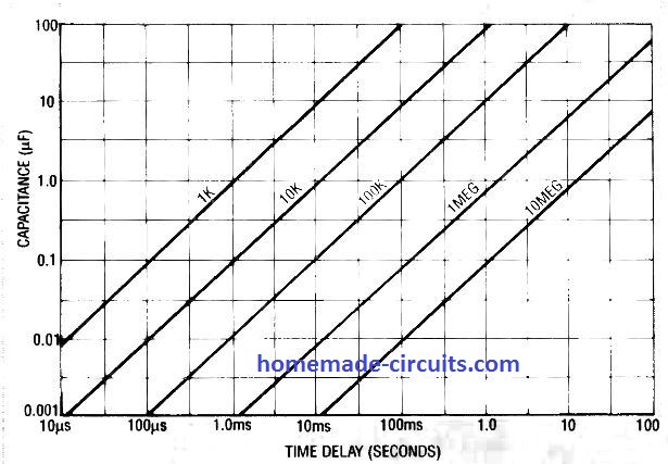
The formula for calculating this is: tD (time delay) = 1.1 (value of R x value of C) In other words the timing interval produced by IC 555 is directly proportional to the product of R and C.
The following graph shows the plotting of time delay vs. resistance, and capacitance using the above the time delay formula. Here tD is in milliseconds, R is in kilo Ω , and C in μfarads.

It shows a range of time delay curves and the linearly changing values with respect to the corresponding values of RT and C.
It is possible to set delays ranging from 10 µseconds to 100 µseconds by selecting appropriate values of capacitors from 0.001 µF to 100 µF and resistors from 1 k Ω to 10 meg Ω .
Simple IC 555 Timer Circuits
The first figure below shows how to make a IC 555 timer having a fixed period output. Here it is set to 50 seconds.
It is basically an IC 555 monostable design.
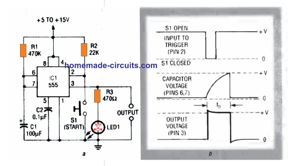
The adjoining figure shows the waveforms obtained across the indicated pinouts of the IC during the switching process.
The actions as described in the waveform image initiates as soon as the TRIGGER pin 2 is grounded with the pressing of momentary START Switch S1.
This instantly causes a rectangular pulse to appear at pin 3 and simultaneously generates an exponential sawtooth at DISCHARGE pin 7.
The time period for which this rectangular pulse remains active is determined by the values of R1, and C1. If R1 is replaced with a variable resistor, this output timing could be set as per user preference.
The LED illumination indicates the ON and OFF switching of the output pin 3 of the IC
The variable resistor can be in the form of a potentiometer as shown in the following figure 2.
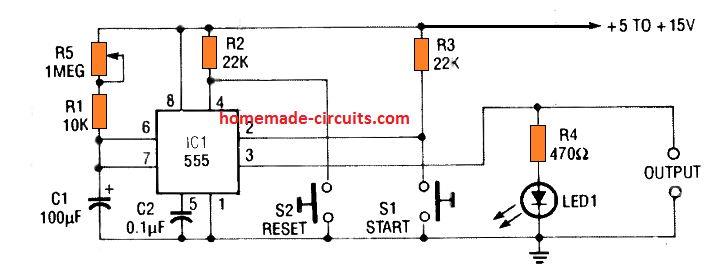
In this design the output can set to produce time periods from 1.1 seconds to 120 seconds through different adjustments of the pot R1.
Notice the series 10K resistor which is very important since it safeguards the IC from burning in case the pot is turned to its lowest value.
The 10 K series resistor also ensures the minimum resistance value required for the correct working of the circuit at the minimum pot setting.
Pressing the switch S1 momentarily enables the IC to start the timing sequence (pin 3 going high and LED turning ON), while pressing S2 reset button allows instant termination or resetting of the timing sequence so that the output pin 3 reverts to its original 0 V situation (LED turning OFF permanently)
The IC 555 allows the use of loads with maximum current specifications of up to 200 mA.
Although these loads are normally non-inductive types, an inductive load like a relay can be also effectively used directly across pin 3 and ground as shown in the following diagrams.
The 3rd figure below we can see that the relay can be wired across pin 3 and ground, and, pin 3 and positive.
Notice the freewheeling diode connected across the relay coil, it is highly recommended for neutralizing the dangerous back emfs from the relay coil during switch OFF instants.
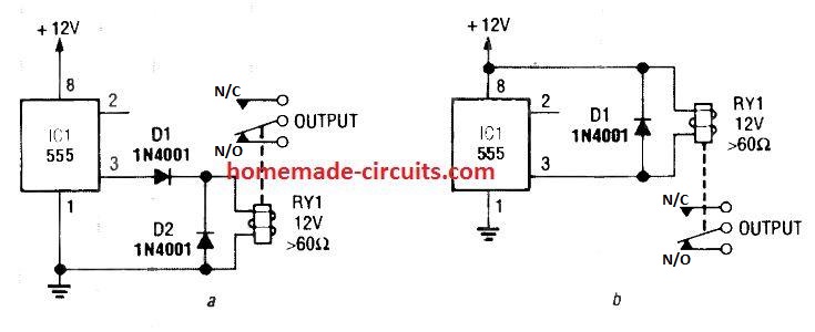
The relay contacts can be wired with an intended load for switching them ON/OFF in response to the set time intervals.
The 4rth circuit diagram shows the standard IC 555 adjustable timer circuit having two sets of timing ranges and an output relay for toggling the desired load.
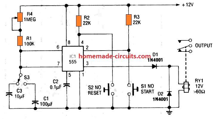
Although the schematic looks correct, this basic circuit may actually have a few negative aspects.
- First, this design will drain some current continuously, even while the output of the circuit is in the off state.
- Second, since the two capacitors C1, and C3 have a wide tolerance specs, the pot neds to be calibrated with two individual set up scales.
The above discussed flaws can be actually overcome, by configuring the circuit in the following manner. Here we use a DPDT relay for the procedures.
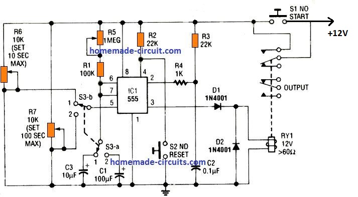
In this 5th IC 555 timer diagram we can see that the relay contacts are joined in parallel with the START switch S1, which are both in the "normally-open" mode, and ensures there's no current drain while the circuit is OFF.
To initiate the timing cycle, S1 is pressed momentarily.
This instantly powers the IC 555. At the onset, C2 can be expected to be fully discharged. Due to this, a negative switch ON trigger is created at pin 2 of the IC, which initiates the timing cycle, and the relay RY1 switches ON.
The relay contacts which are connected in parallel with S1 enables the IC 555 to remain powered even after S2 is released.
When the set time period elapses, the relay is deactivated and its contacts revert to the N/C position disconnecting power from the entire circuit.
The timing delay output of the circuit is basically determined by R1 and potentiometer R5 values, along with the values of either C1 or C2, and depending on the position of the selector switch S3 a.
Having said this, we must also note that the timing is additionally affected by how the potentiometers R6 and R7 are adjusted.
They are switched through the switch S3 b and integrated with the CONTROL voltage pin 5 of the IC.
These potentiometers are introduced to effectively shunt the internal voltage of the IC 555, which might otherwise disturb the output timing of the system.
Due to this enhancement the circuit is now able to function with utmost accuracy even with capacitors having inconsistent tolerance levels.
Furthermore, the feature also allows the circuit to work with a solitary timing scale calibrated to read two individual timing ranges as per the positioning of the selector switch.
For setting up the above accurate IC 555 timer circuit, R5 must be initially adjusted to it maximum range. After this, S3 may be selected to position 1.
Next, adjust R6 to get a 10 second ON timing output scale with some trial and error. Follow the same procedures for the position 2 selection, through the pot R7 for getting an accurate scale of 100 seconds
Timers for car lights
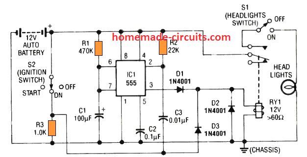
This 6th simple car headlight IC 555 based timer prevents the car headlights from shutting off as soon as the ignition is turned OFF.
Instead, the headlights are allowed to remain illuminated for some preset delay, once the driver locks the car ignition and walks off towards his destination which may be his home or office.
This allows the owner to see the path and enter the destination comfortably with visible illumination from the headlights.
Subsequently, when the delay period elapses the IC 555 circuit switches off the headlights.
How it Works
When the ignition switch S2 is turned ON, the relay RY1 energizes via D3. The relay enables the headlight operations via the upper relay contacts and the switch S1, so that the headlights works normally through S1.
At this point the capacitor C3 associated with pin 2 of the IC remains completely discharged because both its leads are at the positive potential.
However, when the ignition switch S2 is turned OFF, the C3 capacitor is subjected to a ground potential via the relay coil, which suddenly causes a negative trigger to appear at pin 2.
This triggers ON the IC 555 output pin 3, and allows the relay to remain energized even though the ignition is switched OFF.
Depending on the values of the timing components R1 and C1, the relay stays energized keeping the headlights ON (for 50 seconds), until finally the time period elapses and pin 3 of the IC turns OFF de-energizing the relay and the lights.
The circuit does not create any interference with the usual functioning of the headlights while the car is running.
The next 7th timer circuit shown below is also a car headlight timer which is controlled manually instead of the ignition switch.
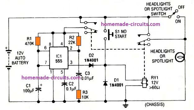
The circuit utilizes a DPDT relay having two sets of contacts. The IC 555 monostable action is initiated by pressing S1 momentarily. This energizes the relay, and both the contacts move upward and connect with the positive supply.
The right side pair of contacts activates the headlights, while the left side contacts power the IC 555 circuit.
The C3 causes a momentary negative pulse to appear at pin 2 which triggers the counting mode of the IC, and pin 3 becomes high latching ON the relay.
The headlights are now switched ON. Depending on the values of R1 and C1 the pin 3 output keeps the relay and the headlights energized (for 50 seconds in this case), until the C1 charges up to the 2/3rd Vcc, turning pin 3 low, and turning Off the relay and the headlights.
1 Minute Porch Light Timer
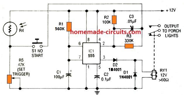
This 8th circuit shows simple porch light timer circuit that can be activated for a minute only during night time. During day time the LDR resistance becomes low which keeps its junction with R5 high.
Due to this, pressing S1 has no effect on pin 2 of the IC. However, when darkness falls, LDR resistance goes infinite, developing an nearly 0 V at the junction of R4 and R5.
In this condition when the switch S1 is pressed, causes a negative trigger at pin 2 of the IC 555, which activates pin 3 to high and also turns ON the relay. The porch light attached with the relay contacts illuminates.
The circuit stays triggered for around 1 minute, until C1 charges to the 2/3rd Vcc. The IC now resets to the turn pin 3 low and de-energizing the relay and switching OFF the porch light.
The switch S1 may be in the form of a small hidden switch near the door handle/hinge, or under the mat which activates when the owner steps on the mat.
Tachometer Application
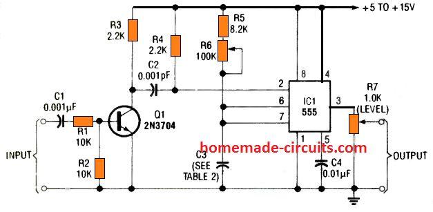
A monostable timer circuit using IC 555 can be also effectively implemented for making a tachometer circuit which will provide the user with accurate information regarding the frequency and engine timing.
The incoming frequency from the engine are first converted to well dimensioned square wave through an RC differentiator network and then fed to pin#2 of the monostable.
The differentiator network transforms the leading or trailing edges of the square wave signal into appropriate trigger pulses.
A 9 th practical circuit below shows how an RC network and a transistor converts any input signal with any amplitude into well formed square waves for generating ideal triggering pulses, switching between the full IC Vcc level and ground.
Mains AC Delay Timer
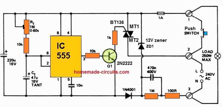
Perfect for an automatic corridor lighting timer, this IC 555 delay timer setup utilizes a momentary action push-button switch with mains rating.
When the switch is pressed, the timer initiates its operation, lasting for a duration precisely equal to 1.1 times the product of R1 and C1.
Once this time elapses, both the load and the entire circuit disconnect simultaneously from mains power.
Conclusion
In all of the circuits presented so far, the 555 functions as a monostable (one-shot) timing period generator. The required trigger signals are fed to TRIGGER pin 2 and a timed pulse at the output pin 3 is delivered.
In all the designs the signal applied at TRIGGER pin 2 are appropriately dimensioned to form a negative edged pulse.
It ensures that the trigger amplitude switches from an "off' level higher than 2/3rd of the supply voltage to an "on" value lower than 1/3rd of the supply level.
Triggering of the IC one shot monostable actually happens when the potential at pin 2 is pulled down to 1/3rd of the supply voltage level.
This requires the trigger pulse width at pin 2 to be higher than 100 nanoseconds but lower than the pulse which is intended to appear at the output pin 3.
This ascertains the elimination of the trigger pulse by the time the set monostable period elapses.


With over 50,000 comments answered so far, this is the only electronics website dedicated to solving all your circuit-related problems. If you’re stuck on a circuit, please leave your question in the comment box, and I will try to solve it ASAP!