The LM2673 series of regulators is a collection of monolithic integrated circuits that are designed to provide all the active functions needed for making a step-down, or buck converter, switching regulator circuit.
This means that they are capable of driving loads of up to 3 amps while maintaining excellent line and load regulation characteristics.
One of the standout features is their high efficiency which is greater than 90%.
This impressive efficiency is achieved thanks to the use of a low ON-resistance DMOS power switch.
Now when it comes to output voltages, this series has you covered with fixed options available at 3.3 V, 5 V, and 12 V, plus there is also an adjustable output version for those who need a bit more flexibility.
The whole idea behind the SIMPLE SWITCHER® concept is to make the design process as straightforward as possible by using a minimal number of external components.
One of the cool things about these regulators is that they operate with a high fixed frequency oscillator running at 260 kHz.
This allows designers to use smaller-sized components, which can be really handy in tight spaces.
Plus there is a family of standard inductors available from various manufacturers that are compatible with the LM2673, making the design process even easier.
Another neat feature is the ability to reduce input surge current when powering on the regulator.
You can do this by adding a soft-start timing capacitor which helps to gradually turn on the regulator instead of hitting it with all the power at once right away.
Safety is also a priority with the LM2673 series since it includes built-in thermal shutdown features and a resistor-programmable current limit for the power MOSFET switch.
This helps protect both the device itself and any load circuitry connected to it under fault conditions.
The output voltage is guaranteed to stay within a ±2% tolerance which is pretty reliable.
Additionally the clock frequency is controlled within a ±11% tolerance.
Pinout Details

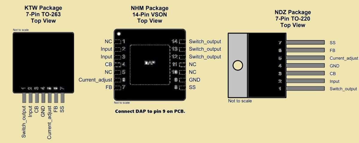
Pinout Functions
| NAME | PIN (TO-263, TO-220) | PIN (VSON) | I/O | DESCRIPTION |
|---|---|---|---|---|
| Switch output | 1 | 12, 13, 14 | O | The internal High Side FET's source pin. This node is used for switching. Connect this pin to the external diode's cathode and an inductor. |
| Input | 2 | 2, 3 | I | Connect the input pin to the high-side FET's collector pin. Attach the input bypass capacitors CIN and power supply. The VIN pin must have the shortest path feasible to the high-frequency bypass CIN and GND. |
| CB | 3 | 4 | I | Connection of the bootstrap capacitor for the high-side driver. A high-grade 100-nF capacitor should be connected from the CB to the VSW pin. |
| GND | 4 | 9 | — | Power ground pins. Connect to the circuit ground. COUT and CIN ground pins. The path to CIN should be as short as feasible. |
| Current adjust | 5 | 6 | I | Adjust the pin for the current limit. If you want to set the part's current limit, attach a resistor from this pin to GND. |
| FB (Feedback) | 6 | 7 | I | input pin for the feedback detection. For an adjustable version, connect this pin to the midway of the feedback divider to set VOUT. For a fixed output version, connect this pin straight to the output capacitor. |
| SS (Soft start) | 7 | 8 | I | Pin that allows for soft start. In order to regulate the output voltage ramp, add a capacitor from this pin to GND. The pin could be left open and floating if the functionality is not wanted. |
| NC (No connect) | — | 1, 5, 10, 11 | — | Unused, No connect pins. |
Absolute Maximum Ratings of the IC LM2673
| Parameter | Min | Max | Unit |
|---|---|---|---|
| Input supply voltage | — | 45 | V |
| Soft-start pin voltage | −0.1 | 6 | V |
| Switch voltage to ground (3) | −1 | VIN | V |
| Boost pin voltage | — | VSW + 8 | V |
| Feedback pin voltage | −0.3 | 14 | V |
| Power dissipation | — | Internally Limited | — |
| Soldering temperature (Wave, 4 s) | — | 260 | °C |
| Soldering temperature (Infrared, 10 s) | — | 240 | °C |
| Soldering temperature (Vapor phase, 75 s) | — | 219 | °C |
| Storage temperature, Tstg | −65 | 150 | °C |
Notes:
Pushing things way past the above Absolute Maximum Ratings can totally wreck your device, like, permanently.
Seriously these ratings are just about stress and don't go thinking your device will actually work if you're pushing it to these limits or even close to the other conditions that aren't inside the Recommended Operating Conditions.
And if you're dealing with Military/Aerospace grade stuff, you got to contact the Texas Instruments Sales Office/Distributors to see what's up and get the right specs.
Also, that Switch Voltage to Ground parameter? That absolute maximum specification is talking about DC voltage.
But you can go a little negative with the voltage, like -10 V but only if it's just a tiny blip of a pulse, like up to 20 ns.
If the pulse is a bit longer, say 60 ns then you can only go down to -6 V, and if it's even longer, like 100 ns, then it's only -3 V...
Recommended Operating Conditions
| Parameter | MIN | MAX | UNIT |
|---|---|---|---|
| Supply Voltage | 8 | 40 | V |
| Junction Temperature (Tj) | -40 | 125 | °C |
Electrical Characteristics
LM2673 - Fixed 3.3 V Output
| Parameter | Test Conditions | MIN | TYP | MAX | UNIT |
|---|---|---|---|---|---|
| Output Voltage (Vout) | Vin = 8 V to 40 V, 100 mA ≤ Iout ≤ 5 A over -40°C to 125°C | 3.234 | 3.3 | 3.366 | V |
| Efficiency (η) | Vin = 12 V, Iload = 5 A | 3.201 | 3.399 | % |
LM2673 - Fixed 5 V Output
| Parameter | Test Conditions | MIN | TYP | MAX | UNIT |
|---|---|---|---|---|---|
| Output Voltage (Vout) | Vin = 8 V to 40 V, 100 mA ≤ Iout ≤ 5 A over -40°C to 125°C | 4.9 | 5 | 5.1 | V |
| Efficiency (η) | Vin = 12 V, Iload = 5 A | 4.85 | 5.15 | % |
LM2673 - Fixed 12 V Output
| Parameter | Test Conditions | MIN | TYP | MAX | UNIT |
|---|---|---|---|---|---|
| Output Voltage (Vout) | Vin = 15 V to 40 V, 100 mA ≤ Iout ≤ 5 A over -40°C to 125°C | 11.76 | 12 | 12.24 | V |
| Efficiency (η) | Vin = 24 V, Iload = 5 A | 11.64 | 12.36 | % |
LM2673 - Adjustable Output 8V to 40V
| Parameter | Test Conditions | MIN | TYP | MAX | UNIT |
|---|---|---|---|---|---|
| Feedback Voltage (Vfb) | Vin = 8 V to 40 V, 100 mA ≤ Iout ≤ 5 A over -40°C to 125°C | 1.186 | 1.21 | 1.234 | V |
| Efficiency (η) | Vin = 12 V, Iload = 5 A | 1.174 | 1.246 | % |
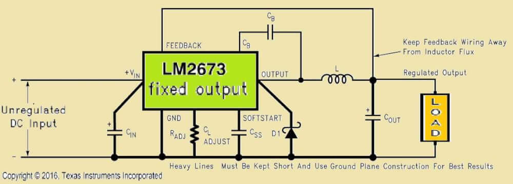
Detailed Description (Typical Fixed Voltage Output Design)
The LM2673 is a fantastic little piece of technology that provides all the active functions you need for a step-down, or buck converter, switching regulator.
It features an internal power switch that is actually a DMOS power MOSFET. This design allows it to handle high current capabilities—up to 3 A—while operating with impressive efficiency.
If you are looking for design support, the WEBENCH tool is super handy. It can help you with instant component selection, perform circuit performance calculations for evaluation, generate a bill of materials component list, and even provide a circuit schematic specifically for the LM2673.
Functional Block Diagram
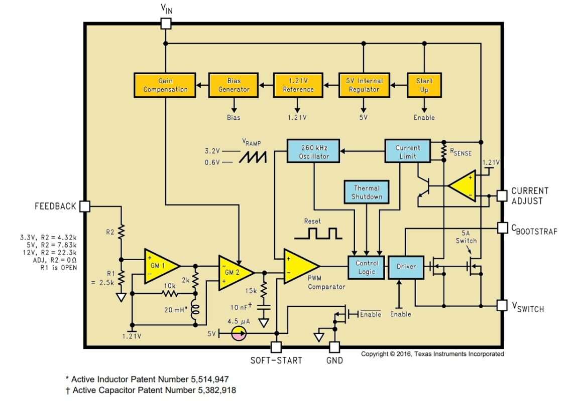
Switch Output
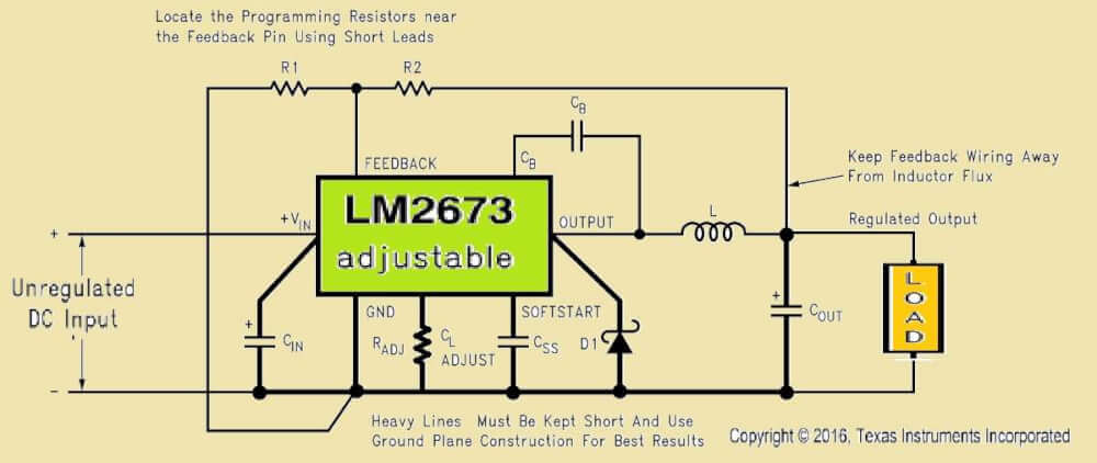
Let us talk about the switch output for a moment. This output comes directly from a power MOSFET switch that is connected right to the input voltage.
What this switch does is provide energy to an inductor, an output capacitor, and the load circuitry, all under the control of an internal pulse-width modulator (PWM).
The PWM controller operates off a fixed 260 kHz oscillator. In a typical step-down application, the duty cycle—essentially the ratio of time the switch is ON versus OFF—of this power switch is proportional to the ratio of the output voltage of the power supply compared to the input voltage.
You will find that the voltage on pin 1 switches between VIN (when the switch is ON) and below ground level due to the voltage drop across an external Schottky diode (when the switch is OFF).
Input
Now moving on to the input side, this is where you connect your input voltage for the power supply at pin 2. Not only does this input voltage provide energy to your load, but it also supplies bias for all of the internal circuitry within the LM2673.
To ensure everything works as it should, make sure that your input voltage stays within the range of 8 V to 40 V. For optimal performance from your power supply, it is crucial to always bypass this input pin with an input capacitor that is placed close to pin 2.
C Boost
Next up is C Boost. You need to connect a capacitor from pin 3 to the switch output at pin 1. This capacitor plays an important role by boosting the gate drive to that internal MOSFET above VIN so that it can fully turn ON.
By doing this it helps minimize conduction losses in the power switch which in turn maintains high efficiency. The recommended value for this CBoost capacitor is around 0.01 µF.
Ground
Let us not forget about ground! This connection serves as the ground reference for all components in your power supply setup.
In applications where you have fast-switching and high currents—like those using the LM2673—Texas Instruments recommends using a broad ground plane.
This helps minimize signal coupling throughout your circuit and keeps everything running smoothly.
Current Adjust
One of the standout features of the LM2673 is its ability to adjust and tailor the peak switch current limit according to what your specific application requires.
This means you do not have to worry about using external components that need to be physically sized to handle current levels that might be much higher than what your circuit normally operates at (like during shorted output conditions).
To set this up you connect a resistor from pin 5 to ground. This resistor establishes a current (I(pin 5) = 1.2 V / RADJ) that determines how much peak current flows through that power switch. The maximum switch current gets fixed at a level calculated as 37,125 divided by RADJ.
Feedback
Now let us move on to feedback. This input connects to a two-stage high-gain amplifier that drives the PWM controller. It is essential to connect pin 6 directly to the actual output of your power supply in order to set that DC output voltage correctly.
For fixed output devices like those with outputs of 3.3 V, 5 V, and 12 V, you only need a direct wire connection to get it done since there are internal gain-setting resistors already provided inside the LM2673.
However if you are using an adjustable output version you will need two external resistors in order to set that DC output voltage accurately.
To ensure stable operation of your power supply, it is really important to prevent any coupling of inductor flux into the feedback input.
Soft-Start
Finally we have soft-start! By connecting a capacitor from pin 7 to ground, you allow for a gradual turn-on of your switching regulator.
This capacitor sets up a time delay that gradually increases how much duty cycle your internal power switch uses.
This feature can significantly reduce how much surge current gets pulled from your input supply when there is an abrupt application of input voltage.
If you do not need soft-start functionality then you should leave this pin open-circuited.
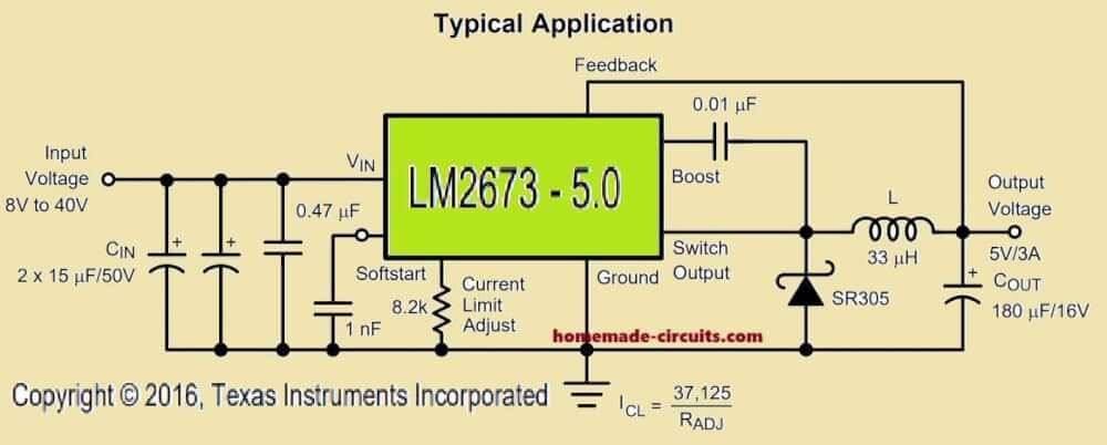
Designing a LM2673 Sep-Down Regulator with Fixed Voltage Output
Design Requirements
So if you are looking to get the LM2673 up and running, you will need to nail down a few things first. Start by figuring out the power supply operating conditions and the maximum output current you will need. Then follow these steps to pick out the right external components for your LM2673 setup.
Detailed Design Procedure
Let us imagine you want to create a system logic power supply bus that runs at 3.3 V. You are planning to use a wall adapter that gives you an unregulated DC voltage somewhere between 13 V and 16 V. Also the maximum load current you expect is around 2.5 A.
Oh and you would like a soft-start delay time of about 50 ms. Plus you prefer using through-hole components.
Okay here is how we can make it happen:
Step 1: Operating Conditions
First let us lay out the known operating conditions:
- VOUT = 3.3 V
- VIN maximum = 16 V
- ILOAD maximum = 2.5 A
Step 2: Select the LM2673 Variant
Go ahead and pick an LM2673T-3.3. Keep in mind that the output voltage has a tolerance of ±2% at room temperature and ±3% over the full operating temperature range.
Step 3: Choose Your Inductor
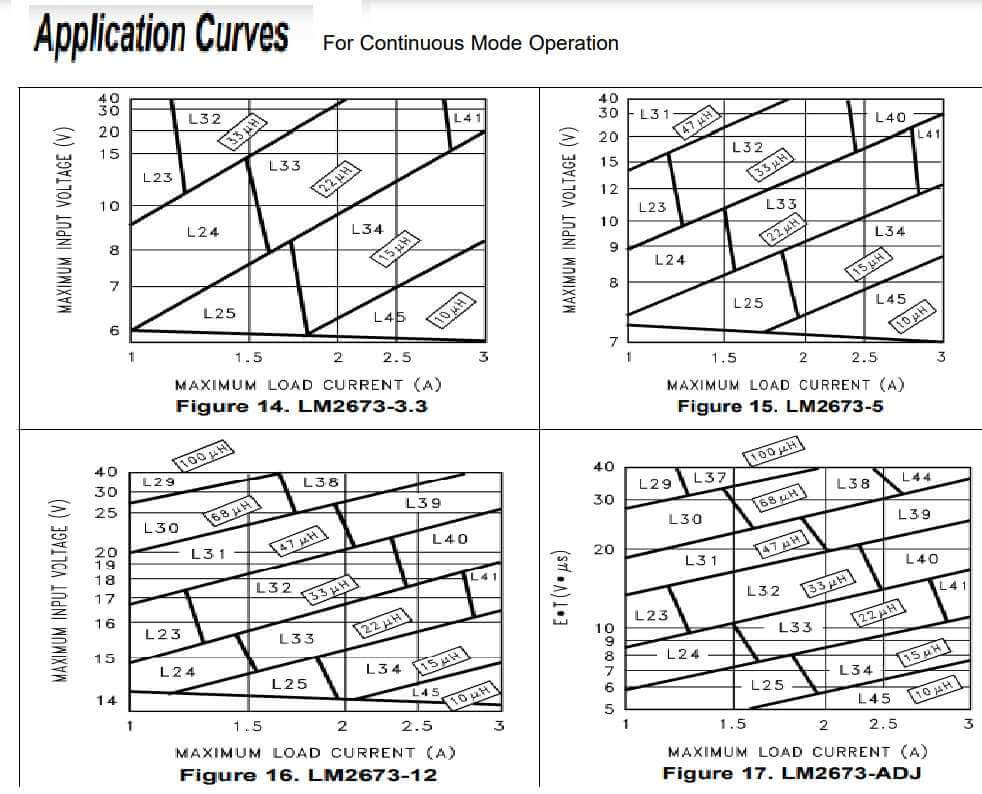
Now let us use the nomograph for the 3.3 V device. Find Figure 14 (though it is not included in these search results, this step assumes you have access to it) and see where the 16 V horizontal line (VIN max) intersects with the 2.5 A vertical line (ILOAD max). This intersection point tells you that you will need an L33, which is a 22 µH inductor.
Looking at Table 3 (also not included in these search results but assumed to be available), you will see that the L33 in a through-hole component can be sourced from Renco with part number RL-1283-22-43 or from Pulse Engineering with part number PE-53933.
Step 4: Pick Your Output Capacitor
Next use Table 5 or Table 6 (again, these tables are not provided here but are assumed to be accessible) to figure out which output capacitor to use. Given that you have a 3.3 V output and a 33 µH inductor, there should be several through-hole output capacitor solutions.
These solutions will tell you how many of the same type of capacitors to parallel and will give you an identifying capacitor code.
Table 1 or Table 2 (also assumed to be available) should provide the specific characteristics for each capacitor. Any of these choices would work well in your circuit:
- 1 × 220 µF, 10 V Sanyo OS-CON (code C5)
- 1 × 1000 µF, 35 V Sanyo MV-GX (code C10)
- 1 × 2200 µF, 10 V Nichicon PL (code C5)
- 1 × 1000 µF, 35 V Panasonic HFQ (code C7)
Table 1. Input and Output Capacitor Codes—Surface Mount
| Capacitor Reference Code | AVX TPS Series | SPRAGUE 594D Series | KEMET T495 Series |
|---|---|---|---|
| C (μF) | WV (V) | Irms (A) | |
| C1 | 330 | 6.3 | 1.15 |
| C2 | 100 | 10 | 1.1 |
| C3 | 220 | 10 | 1.15 |
| C4 | 47 | 16 | 0.89 |
| C5 | 100 | 16 | 1.15 |
| C6 | 33 | 20 | 0.77 |
| C7 | 68 | 20 | 0.94 |
| C8 | 22 | 25 | 0.77 |
| C9 | 22 | 35 | 0.63 |
| C10 | 22 | 35 | 0.66 |
| C11 | — | — | — |
| C12 | — | — | — |
| C13 | — | — | — |
Table 2. Input and Output Capacitor Codes—Through Hole
| Capacitor Reference Code | Sanyo OS-CON SA Series | Sanyo MV-GX Series | Nichicon PL Series | Panasonic HFQ Series |
|---|---|---|---|---|
| C (μF) | WV (V) | Irms (A) | C (μF) | |
| C1 | 47 | 6.3 | 1 | 1000 |
| C2 | 150 | 6.3 | 1.95 | 270 |
| C3 | 330 | 6.3 | 2.45 | 470 |
| C4 | 100 | 10 | 1.87 | 560 |
| C5 | 220 | 10 | 2.36 | 820 |
| C6 | 33 | 16 | 0.96 | 1000 |
| C7 | 100 | 16 | 1.92 | 150 |
| C8 | 150 | 16 | 2.28 | 470 |
| C9 | 100 | 20 | 2.25 | 680 |
| C10 | 47 | 25 | 2.09 | 1000 |
| C11 | — | — | — | 220 |
| C12 | — | — | — | 470 |
| C13 | — | — | — | 680 |
| C14 | — | — | — | 1000 |
| C15 | — | — | — | — |
| C16 | — | — | — | — |
| C17 | — | — | — | — |
| C18 | — | — | — | — |
| C19 | — | — | — | — |
| C20 | — | — | — | — |
| C21 | — | — | — | — |
| C22 | — | — | — | — |
| C23 | — | — | — | — |
| C24 | — | — | — | — |
| C25 | — | — | — | — |
Inductor Selection Guide
Table 3. Inductor Manufacturer Part Numbers
| INDUCTOR REFERENCE NUMBER | INDUCTANCE (µH) | CURRENT (A) | RENCO THROUGH HOLE | RENCO SURFACE MOUNT | PULSE ENGINEERING THROUGH HOLE | PULSE ENGINEERING SURFACE MOUNT | COILCRAFT SURFACE MOUNT |
|---|---|---|---|---|---|---|---|
| L23 | 33 | 1.35 | RL-5471-7 | RL1500-33 | PE-53823 | PE-53823S | DO3316-333 |
| L24 | 22 | 1.65 | RL-1283-22-43 | RL1500-22 | PE-53824 | PE-53824S | DO3316-223 |
| L25 | 15 | 2 | RL-1283-15-43 | RL1500-15 | PE-53825 | PE-53825S | DO3316-153 |
| L29 | 100 | 1.41 | RL-5471-4 | RL-6050-100 | PE-53829 | PE-53829S | DO5022P-104 |
| L30 | 68 | 1.71 | RL-5471-5 | RL6050-68 | PE-53830 | PE-53830S | DO5022P-683 |
| L31 | 47 | 2.06 | RL-5471-6 | RL6050-47 | PE-53831 | PE-53831S | DO5022P-473 |
| L32 | 33 | 2.46 | RL-5471-7 | RL6050-33 | PE-53932 | PE-53932S | DO5022P-333 |
| L33 | 22 | 3.02 | RL-1283-22-43 | RL6050-22 | PE-53933 | PE-53933S | DO5022P-223 |
| L34 | 15 | 3.65 | RL-1283-15-43 | — | PE-53934 | PE-53934S | DO5022P-153 |
| L38 | 68 | 2.97 | RL-5472-2 | — | PE-54038 | PE-54038S | — |
| L39 | 47 | 3.57 | RL-5472-3 | — | PE-54039 | PE-54039S | — |
| L40 | 33 | 4.26 | RL-1283-33-43 | — | PE-54040 | PE-54040S | — |
| L41 | 22 | 5.22 | RL-1283-22-43 | — | PE-54041 | P0841 | — |
| L44 | 68 | 3.45 | RL-5473-3 | — | PE-54044 | P0845 | DO5022P-103HC |
| L45 | 10 | 4.47 | RL-1283-10-43 | — | PE-54044 |
Table 4. Schottky Diode Selection Table
| REVERSE VOLTAGE (V) | SURFACE MOUNT | THROUGH HOLE | ||
|---|---|---|---|---|
| 3 A | 5 A OR MORE | 3 A | 5 A OR MORE | |
| 20 | SK32 | — | 1N5820 | — |
| — | — | SR302 | — | |
| 30 | SK33 | MBRD835L | 1N5821 | — |
| 30WQ03F | — | 31DQ03 | — | |
| 40 | SK34 | MBRB1545CT | 1N5822 | — |
| 30BQ040 | — | MBR340 | MBR745 | |
| 30WQ04F | 6TQ045S | 31DQ04 | 80SQ045 | |
| MBRS340 | — | SR403 | 6TQ045 | |
| MBRD340 | — | — | — | |
| 50 or more | SK35 | — | MBR350 | — |
| 30WQ05F | — | 31DQ05 | — | |
| — | — | SR305 | — |
Nomographs
Step 5: Select Your Input Capacitor
Finally use Table 5 or Table 8 to pick out an input capacitor. With a 3.3 V output and a 22 µH inductor, there are three through-hole solutions available.
These capacitors will give you a sufficient voltage rating and an RMS current rating that is greater than 1.25 A (which is half of ILOAD max).
Again referring to Table 1 or Table 2 for specific component details, these options are suitable:
- 1 × 1000 µF, 63 V Sanyo MV-GX (code C14)
- 1 × 820 µF, 63 V Nichicon PL (code C24)
- 1 × 560 µF, 50 V Panasonic HFQ (code C13)
Step 6: Select a Schottky Diode
Now take a peek at Table 4. You will need to pick out a Schottky diode that is rated for 3 amps or more. For this application, where we are dealing with voltages around 20 V, there are a couple of suitable through-hole components you could use:
1N5820
SR302
Step 7: Setting Up CBOOST and Soft-Start
Next let us get that CBOOST capacitor sorted out. You can go with a 0.01 µF capacitor for CBOOST.
Now for that 50 ms soft-start delay you wanted, we are going to need to consider a few parameters:
- ISST: 3.7 µA
- tSS: 50 mS
- VSST: 0.63 V
- VOUT: 3.3 V
- VSCHOTTKY: 0.5 V
- VIN: 16 V
By using the maximum VIN value, you are making sure that the soft-start delay time will be at least the 50 ms you are aiming for.
To figure out the right value for CSS, you can use the formula (but I am not formatting it here, so you can see it in plain text) and that gives us a value of 0.148 µF. Since that is not a standard capacitor value, you can use a 0.22 µF capacitor instead. This will give you more than enough soft-start delay.
Step 8: Determine RADJ Value
Finally let us figure out the value for RADJ to set the peak switch current limit. You want this limit to be at least 2.5 A, plus an extra 50% for safety, which means we are shooting for 3.75 A.
You can use the following formula to figure out RADJ:
RADJ = 37125 / 3.75A = 9.9 kΩ
So a value of 10 kΩ should work nicely.
Capacitor Selection
Table 5. Output Capacitors for Fixed Output Voltage Application—Surface Mount
| OUTPUT VOLTAGE (V) | INDUCTANCE (µH) | AVX TPS SERIES | SPRAGUE 594D SERIES | KEMET T495 SERIES | |||
|---|---|---|---|---|---|---|---|
| NO. | C CODE | NO. | C CODE | NO. | C CODE | ||
| 3.3 | 10 | 4 | C2 | 3 | C1 | 4 | C4 |
| 15 | 4 | C2 | 3 | C1 | 4 | C4 | |
| 22 | 3 | C2 | 2 | C7 | 3 | C4 | |
| 33 | 2 | C2 | 2 | C6 | 2 | C4 | |
| 5 | 10 | 4 | C2 | 4 | C6 | 4 | C4 |
| 15 | 3 | C2 | 3 | C7 | 3 | C4 | |
| 22 | 3 | C2 | 2 | C7 | 3 | C4 | |
| 33 | 2 | C2 | 2 | C3 | 2 | C4 | |
| 47 | 2 | C2 | 1 | C7 | 2 | C4 | |
| 12 | 10 | 4 | C5 | 3 | C6 | 5 | C9 |
| 15 | 3 | C5 | 2 | C7 | 4 | C8 | |
| 22 | 2 | C5 | 2 | C6 | 3 | C8 | |
| 33 | 2 | C5 | 2 | C6 | 2 | C8 | |
| 47 | 2 | C5 | 1 | C5 | 2 | C8 | |
| 68 | 1 | C4 | 1 | C5 | 1 | C7 | |
| 100 | 1 | C4 | 1 | C5 | 1 | C8 |
Designing a LM2673 Sep-Down Regulator with an Adjustable Voltage Output
So like, first off, you got to know what kind of power you're working' with and what you want out of this thing.
Then we will move through the steps to select the right parts for the LM2673.
Step 1: Figure out the operating conditions: What is your VOUT (that's voltage out) whats the highest your VIN (voltage in) will be, and what's the max ILOAD (current load) you're expecting?
Like say you're getting the input supply from a truck's two batteries (20V to 28V) to step down the voltage to a more normal 14.8V for gadgets.
And, say those gadgets need 2A max.
Step 2: Pick an LM2673S-ADJ. To get that output voltage to 14.8V you'll need a couple of resistors (we're talking R1 and R2).
Here's the formula to keep in your pocket:
VOUT = VFB(1 + (R2/R1)),
VFB is usually around 1.21V.
A good pick for R1 is 1kΩ.
To find R2 it's going to be: R2 = R1 * ((VOUT / VFB) - 1) = 1 kΩ * ((14.
8 V / 1.21 V) - 1)
That makes R2 about 11.23 kΩ.
A close standard value is 11.3 kΩ.
Step 3: To figure out the inductor, use the nomograph.
You need to figure out the Volt-microsecond constant (E * T):
E * T = (VIN(MAX) - VOUT - VSAT) * (VOUT + VD) / (VIN(MAX) - VSAT + VD) * (1000 / 260) (V * μs),
VSAT is the voltage drop across the internal power switch, which is about Rds(ON) times ILOAD,
VD is the voltage drop across the Schottky diode (around 0.5 V).
Plugging in the above numbers gives:
E * T = (28 - 14.8 - 0.3) * (14.8 + 0.5) / (28 - 0.3 + 0.5) * (1000 / 260) (V * μs),
E * T = (12.9 V) * (15.3 / 28.2) * 3.85 (V * μs) = 26.9 (V * μs),
With that you'll probably need a 68 µH inductor.
Step 4: Peep the tables to pick an output capacitor.
With a 14.8V output and a 68-µH inductor, you have choices like: 1 × 33 µF, 20-V AVX TPS, 1 × 47 µF, 20 V Sprague 594, 1 × 47 µF, 20 V Kemet T495.
If the nomograph Figure 17 chooses an inductance of 22 µH or less when employing the adjustable device in low voltage applications (meaning less than 3-V output), Tables 9 and 10 do not offer an output capacitor option. The quantity of output capacitors needed for consistent functioning turns unattainable under these circumstances. A 33-µH or 47-µH inductor and the output capacitors from Tables 9 or 10 are suggested by TI.
Step 5: You will want an input capacitor that's at least 35V and can handle an RMS current of 1A. See Table 1 or Table 2
A 33 µF, 35 V cap should work.
Step 6: Snag a 3 A Schottky diode. See Table 4 for this. Some surface mount options could be: SK34, 30BQ040, 30WQ04F, MBRS340, MBRD340.
Step 7: For the CBOOST, you're going to need a 0.01 µF capacitor.
And that soft-start pin? Just leave it hanging, don't connect it to anything.
Step 8: Then you got to figure out RADJ.
You want it so the peak current is like, 2 amps plus half of that, so 3 amps total.
The formula is
RADJ = 37125/3 = 12.375 k Ohms.
So use a 12.4 kΩ resistor.
For more information on this project and the complete guide please visit the ti.com website
Have Questions? Please Leave a Comment. I have answered over 50,000. Kindly ensure the comments are related to the above topic.