An audio delay line is a technique in which a given audio signal is passed through a series of digital storage stages, until the final audio output is delayed by a certain period (usually in milliseconds). When this delayed audio output is fed back to the original audio, it results in an amazingly enhanced audio, which is richer, more voluminous, and stuffed with features like echo and reverb.
Overview
The listening experience for a music played inside a room depends significantly on the interiors of the room.
If the room interior is filled with many modern decors and glass windows, that might create too much echo effect on the music.
On the other hand, if the room includes a lot of fabric based elements like heavy curtains, cushioned furniture etc, the music will tend to loss all echo and reverb effects, and might sound quite dull and uninteresting.
For the latter case, you can probably choose to discard and throw away all curtains, pillows, cushions, sofa set, or opt for the proposed audio delay line circuit, which will help you to restore the ambiance of the music naturally without sacrificing your favorite interiors.
Through this circuit you can actually generate an echo (audio signal time delay) and reverberation (after reflections) and accomplish a much richer audio.
Until not too long ago, the sole technique of acquiring an audio signal delay was by using very costly electronic devices. Today we have a brand new form of IC, called the "bucket-brigade" which allows you to construct your personal delay system very cheaply.
Attached between the audio source and the preamp, or between the preamp and the power amplifier, the concept offers a variable signal echo, which could enrich the sound from most home music systems.
With a small circuit modifications, the idea additionally could be applied as a phasor/flanger, allowing the user to get sound effects for recording applications and for electric guitars utilized by the specialists.
The bucket-brigade IC is a MOStype shift register consisting of two 512 -stage registers in a solitary 14-pin package.
If an audio signal is fed to the input of the bucket-brigade design, and the relevant ICs driven with a clock generator, causes the audio signal to move in a stepped manner, stage by stage, until finally the signal arrives at the output with the intended delay.
The block diagram for the delay line circuit is shown below:
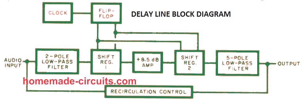
When this delayed signal is fed back (recirculated) into the original signal, a reverberation effect is simulated.
Besides delivering real-time ambiance, the bucket-brigade circuit could be implemented with any audio system to produce synthetic stereo sound from mono audio sources, an useful option for "double voicing," and "phasor/flanging."
What is Bucket Brigade
The term "bucket brigade" reminds us of a line of men handing buckets of water to combat a fire hazard.
The bucket-brigade analog shift register functions in an identical manner, and hence the name.
With shift registers, on the other hand, the capacitors represent the "buckets" connected directly on the PMOS IC. There can be in excess of 1000 such capacitors on every single chip (a single capacitor and a couple of MOS transistors per stage).
The element that is being passed along are actually the packets of electrical charge across one stage to the next. We know that It is not easy to put water evenly into and from a bucket simultaneously.
In the same way, it is not easy to simultaneously charge and discharge a capacitor. This issue is resolved by the shift registers, and through of a pair of out-of-phase clocks frequencies.
During the period when the first clock is high, the buckets with the "odd" figures are thrown out to the subsequent buckets with "even" figures. As soon as the second high clock arrives, the even buckets are thrown out into the following successive odd buckets.
This way, individual charges are shifted across the line from one stage one at a time.

The above image is a schematic manifestation of 4 standard stages of the MN3001 analog shift register.
Each MN3001 IC consists of two 512 -stage shift registers. Remember that stages A and C are linked to one particular clock, while stages B and D are coupled to the other clock to deliver the odd/even relationship.
How Delay Line Circuit Works
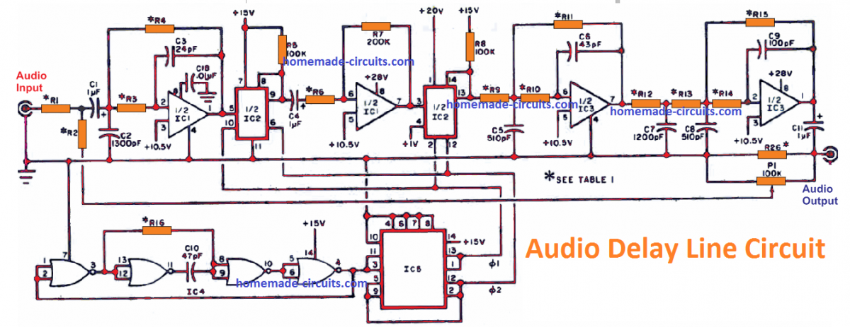
The following schematic shows the complete schematic for the audio delay line.

When you actually create a delay in an audio signal, you generate a variety of interesting audio effects. The most noticeable is the simulation of echo effect.
However, delays created by the bucket brigade are usually very small to be recognized as discrete echoes.
Repeating the delayed signal with diminished gain could mimic the healthy decay of echoes in a reverberant space.
By introducing certain gain throughout the re-circulation of the delayed signal, it may be possible to generate an unnatural "door-spring" outcome for the music.
Causing delay to an instrumental signal or speech track by 30 or 40 ms and pushing the delayed signal back to the original signal, will produce the output audio more voluminous and provide it the impression of having more than the initial quantity of voices or musical depth.
This kind of popular approach is called "double-voicing." Another well-known short-delay effect can be in the form of a peculiar sound that arises through a technique called "phasing" or "reel-flanging."
The title comes from its original experimentation in which a tape recorder had been employed to generate the time delay, and the rubbing of a skilled hand on the outer side of the tape-feed reel altered the delay to generate the acoustic effect.
Today, this effect could be developed entirely through digital technology, by delaying the signal 0.5 to 5 ms while adding or subtracting the delayed signal from the original signal.
In the phasor/flanger setting, the frequency and its harmonics whose wavelengths are identical to the time delay, happens to be fully terminated, while all the other frequencies become strengthened.
In this manner a comb filter having a frequency between the notches is modified by changing the clock frequency, as shown below.
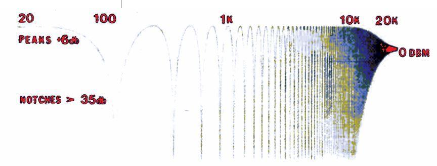
The result is, a tonal improvement introduced to a non-tonal audio, for example drums, cymbals, as well as to vocal frequencies.
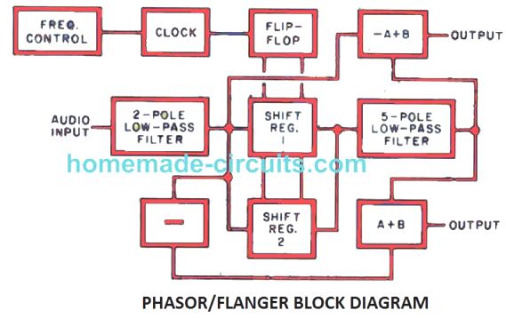
The phasor/flanger mode enables you to replicate stereophonic signals from a monophonic origin. To achieve this, the phased output extracted by introducing the delayed signal is sent to one channel, while the output extracted by subtracting the delayed signal is sent to the opposite.
For the audience, the phasing effect cancels out, allowing a good synthetic stereo effect to their ears.
The main elements of the designs, undoubtedly, are the bucket-brigade IC's, that are able to directly synthesize the analog signals. The circuits do not involve expensive analog-to-digital and digital-to-analog converters.
As soon as the clock pulse from the flipflop is fed to the bucket-brigade IC, the DC supply existing at the input is transferred into the register. The discrete bits are shifted stage by stage through sequential clock pulses until eventually, after 256 pulses, they arrive at the finish of the line and deliver the output signal.
The output waveform is cleaned up with a low-pass filter and whatever duplicate signal had been existing at the input but delayed by 256 times the period of the clock frequency.
For instance, when the clock frequency is 100 kHz, the delay could be 256 x 1/100,000 = 2.56 ms. Considering that the sampling rate of the music signal on the input is dependent on the clock frequency, an assumptive limit of 50% lower clock frequency could be the maximum audio frequency which can be effectively transferred.
Nevertheless, because of real life constraints, 1/3rd of the clock frequency may appear to be a more realistic design objective. Circuits could be sequentially connected or cascaded to offer lengthier time delays at increased clock rates, though the higher noise in the series-connected circuits may possibly outdo the rise in the bandwidth.
In the delay mode, the 2 shift registers are hooked up in series, which enables the use of clock frequencies two times higher.
This allows, two times the bandwidth for each shift register to be programmed for the very same time delay. Even in this double-bandwidth mode, the clock frequency necessary for a 40 ms delay, restricts the bandwidth to a maximum input signal of 3750 Hz, which looks quite enough for voice frequency, although not enough for most musical equipment.
In many applications in which the delayed transmission is implemented to the original signal, the decrease in bandwidth can get concealed due to the high-frequency signals contained in the original signal input. To compensate for normal signal attenuation, an 8.5 dB amplifier is employed between the shift registers.
In the phasor/flanger mode, the highest delay necessary is approximately 5 ms, which is small enough for the use of a single shift register without sacrificing the bandwidth.
The second shift register is consequently attached in parallel with the first to enhance the S/N ratio. The signal frequencies are applied in-phase, while the noise signals get added and deducted at random.
The Phasor/Flanger
The block diagram of the phasor/ flanger designs is shown in the following diagram.
The schematic diagram for the phasor/flanger is given below:
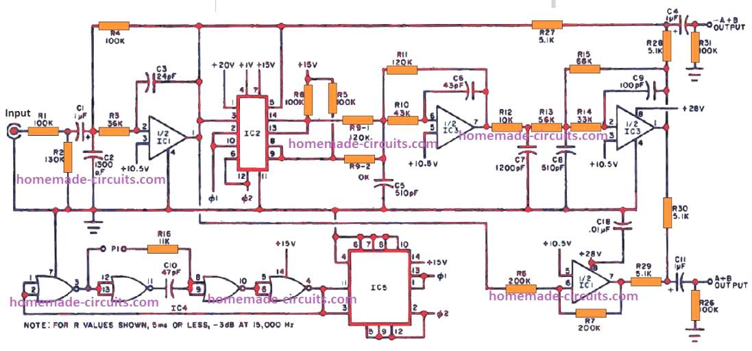

In each scenarios, quad NOR gate IC4 is rigged like astable multivibrator functioning at two times the specified clock rate's frequency.
The IC4 output connects with flip-flop IC5, that offers a couple of contributory (180° out of phase with each other) output clock signals with FIFTY PERCENT duty cycles.
These pulses then act as clock inputs for the shift registers in IC2. Resistor R16 determines the frequency and is a fixed velue in the delay circuit.
The clock frequency could be changed as desired by adding more resistors in parallel through the given connectors in the phasor/flanger.
The audio input signal is processed through seven poles of low-pass filter stages, where IC3 and 1/2 IC1 are utilized. The filters ensure an overall attenuation of 42-dB/octave over a tuned frequency.
As an illustration, when the filter is tuned for 5000 Hz, a 10,000 Hz signal gets attenuated by greater than 100:1.
While the filters are operated with high-gain op amps, you are able to make their outputs maximize before rolling off at 6 dB/octave rate per pole. This kind of filters are called "under damped."
Through proper selection of the balance of under-damped and over-damped (RC) filter stages, it is easy to configure a filter having a flat response in the intended passband, in order to achive 3 dB down on the tuning frequency, and feature a roll-off rate of 6 dB times the quantity of poles.
This is exactly what is implemented in the delay-line and phasor/flanger designs I have I have explained in this article. A substantial amount of statistical working out is usually needed to identify the resistor values for the filters.
To make things easier, you could pick out the suitable resistor values from the Table of Filter Resistor Values.
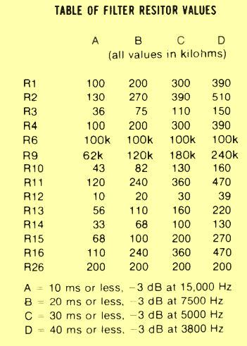
Take advantage of this Table for choosing resistor values specifically for the delay-line circuit. (The filter resistor values given in Fig. 4 and its associated Bill of materials will give you an enhanced 5 ms delay, with the output 3 dB down at 15 kHz for the phasor/flanger.)
Power Supply
Parts List
C12 - 470 µF, 35 V
C13,C15,C16 - 0.01 uF disc capacitor, C14 -100 pF disc capacitor
C17 - 33 µF, 25 V
D1,D2 - IN4007
D3 -1N968 (20 V) zener diode
F1 -1/10 -ampere fuse
IC6 -723 precision voltage regulator
All resistors are I/4 watt 5% tolerance:
R17-1k
R18 - 1M
RI9 - 10 ohms
R20 - 8.2k ohms
R21 - 7.5k ohms
R22 - 33k ohms
R23 - 2.4k
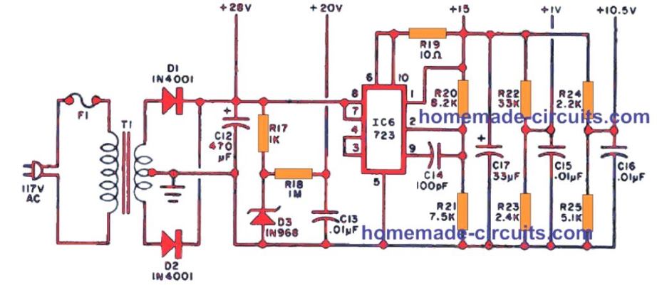
The power supply circuit for the audio delay line is shown in the above image. It is built around a voltage regulator, IC6, to crank out the primary 15 volt supply output. The shift register involves sources of each +1 and +20 volts.
The +20 volt rail is acquired by using zener diode D3, and the +1 volt line comes from the voltage divider configured around R22 and R23.
As the op amps are driven through a single-ended supply, it becomes essential to have the 10.5 volt voltage line function as the reference in the circuit for these devices.
Construction
The real dimension etching and drilling manual, and the very same for both circuit layouts but wired up in a different way as necessary, is demonstrated in the figures below.
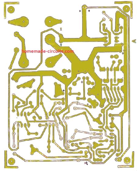
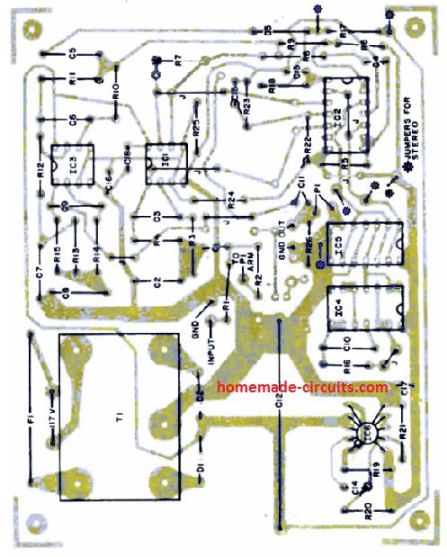
Prior to fitting any parts on the PCB, you should insert and solder the various jumpers links into the slots. After that, connect the board as specified in above, according to the preferred mode of operation.
Be careful about the pin orientation of all the semiconductor devices and electrolytic capacitors, and insert them correctly.
Make sure to hold and assemble the MOS devices with care since these are sensitive to static charges, and may get damaged by the static charge developed on your fingers. You could insert the IC's straight on the PCB or also make use of IC sockets.
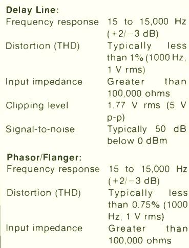
Main Specifications of the proposed Audio Delay Line Circuit
