The LP8864-Q1 is this cool automotive high-efficiency LED driver that comes with a boost controller.
Basically it is made to efficiently power the LEDs in your car.
It has got these four high-precision current sinks that do something called phase shifting. What is neat is that this phase shifting automatically adjusts based on how many channels we are actually using. So it is flexible depending on the setup.
We can control the LED brightness in a big way using the I²C interface or the PWM input. Think of it like having a dimmer switch but way more precise.
The boost controller also has this adaptive thing going on where it controls the output voltage based on the headroom voltages of the LED current sinks.
What this does is super smart: it cuts down on power consumption by tweaking the boost voltage to be just enough for what we need. It is all about being efficient. Plus the LP8864-Q1 has a wide-range adjustable frequency which helps it avoid messing with the AM radio band. Nobody wants static when they are listening to tunes.
And there is more! The LP8864-Q1 can do hybrid PWM dimming and analog current dimming. This is great because it lowers EMI (electromagnetic interference), makes the LEDs last longer and makes the whole optical system more efficient.
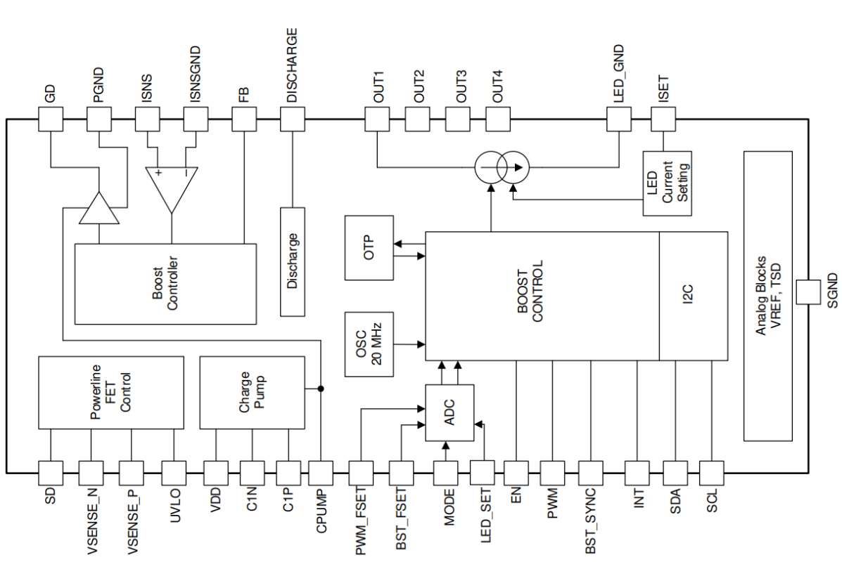
Functional Block Diagram

Pinout Details
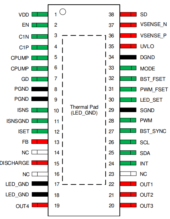
Table 4-1. HTTSOP Pin Functions
| NO. | PIN NAME | TYPE | DESCRIPTION |
|---|---|---|---|
| 1 | VDD | Power | Power input for internal analog and digital circuits. A 10µF capacitor should be connected between VDD and GND. |
| 2 | EN | Analog | Enable input. |
| 3 | C1N | Analog | Negative terminal for the charge pump flying capacitor. Leave floating if not used. |
| 4 | C1P | Analog | Positive terminal for the charge pump flying capacitor. Leave floating if not used. |
| 5 | CPUMP | Analog | Charge pump output pin. Connect to VDD if the charge pump is not used. A 4.7µF decoupling capacitor is recommended. |
| 6 | CPUMP | Analog | Charge pump output pin. Always connected to pin 5. |
| 7 | GD | Analog | Gate driver output for an external N-FET. |
| 8 | PGND | GND | Power ground. |
| 9 | PGND | GND | Power ground. |
| 10 | ISNS | Analog | Boost current sense input. |
| 11 | ISNSGND | GND | Ground for the current sense resistor. |
| 12 | ISET | Analog | Sets the full-scale LED current using an external resistor. |
| 13 | FB | Analog | Boost feedback input. |
| 14 | NC | N/A | No connection. Leave floating. |
| 15 | DISCHARGE | Analog | Boost output voltage discharge pin. Connect to Boost output. |
| 16 | NC | N/A | No connection. Leave floating. |
| 17 | LED_GND | Analog | LED ground connection. |
| 18 | LED_GND | Analog | LED ground connection. |
| 19 | OUT4 | Analog | LED current sink output. Connect to ground if unused. |
| 20 | OUT3 | Analog | LED current sink output. Connect to ground if unused. |
| 21 | OUT2 | Analog | LED current sink output. Connect to ground if unused. |
| 22 | OUT1 | Analog | LED current sink output. Connect to ground if unused. |
| 23 | NC | N/A | No connection. Leave floating. |
| 24 | INT | Analog | Device fault interrupt output, open drain. A 10kΩ pull-up resistor is recommended. |
| 25 | SDA | Analog | I2C data line (SDA). A 10kΩ pull-up resistor is recommended. |
| 26 | SCL | Analog | I2C clock line (SCL). A 10kΩ pull-up resistor is recommended. |
| 27 | BST_SYNC | Analog | Synchronization input for the boost converter. Connect to ground to disable spread spectrum or to VDD to enable it. |
| 28 | PWM | Analog | PWM input for brightness control. Connect to ground if not used. |
| 29 | SGND | GND | Signal ground. |
| 30 | LED_SET | Analog | LED string configuration input via an external resistor. Do not leave floating. |
| 31 | PWM_FSET | Analog | Sets the dimming frequency via an external resistor. Do not leave floating. |
| 32 | BST_FSET | Analog | Configures the boost switching frequency via an external resistor. Do not leave floating. |
| 33 | MODE | Analog | Sets the dimming mode via an external resistor. Do not leave floating. |
| 34 | DGND | GND | Digital ground. |
| 35 | UVLO | Analog | Input for programming the undervoltage lockout (UVLO) threshold via an external resistor to VIN. |
| 36 | VSENSE_P | Analog | Voltage detection input for overvoltage protection. Also serves as the positive terminal for input current sensing. |
| 37 | VSENSE_N | Analog | Negative input for current sensing. If current sense is not used, connect to VSENSE_P. |
| 38 | SD | Analog | Power line for the FET control. Open drain output. Leave floating if unused. |
| DAP | LED_GND | GND | LED ground connection. |
Table 4-2. QFN Pin Functions
| NO. | PIN NAME | TYPE | DESCRIPTION |
|---|---|---|---|
| 1 | LED_GND | Analog | LED ground connection. |
| 2 | LED_GND | Analog | LED ground connection. |
| 3 | OUT4 | Analog | LED current sink output. Connect to ground if unused. |
| 4 | LED_GND | GND | LED ground connection. |
| 5 | OUT3 | Analog | LED current sink output. Connect to ground if unused. |
| 6 | OUT2 | Analog | LED current sink output. Connect to ground if unused. |
| 7 | OUT1 | Analog | LED current sink output. Connect to ground if unused. |
| 8 | INT | Analog | Device fault interrupt output, open drain. A 10kΩ pull-up resistor is recommended. |
| 9 | SDA | Analog | I2C data line (SDA). A 10kΩ pull-up resistor is recommended. |
| 10 | SCL | Analog | I2C clock line (SCL). A 10kΩ pull-up resistor is recommended. |
| 11 | BST_SYNC | Analog | Synchronization input for the boost converter. Connect to ground to disable spread spectrum or to VDD to enable it. |
| 12 | PWM | Analog | PWM input for brightness control. Connect to ground if not used. |
| 13 | SGND | GND | Signal ground. |
| 14 | LED_SET | Analog | LED string configuration input via an external resistor. Do not leave floating. |
| 15 | PWM_FSET | Analog | Sets the dimming frequency via an external resistor. Do not leave floating. |
| 16 | BST_FSET | Analog | Configures the boost switching frequency via an external resistor. Do not leave floating. |
| 17 | MODE | Analog | Sets the dimming mode via an external resistor. Do not leave floating. |
| 18 | UVLO | Analog | Input for programming the undervoltage lockout (UVLO) threshold via an external resistor to VIN. |
| 19 | VSENSE_P | Analog | Voltage detection input for overvoltage protection. Also serves as the positive terminal for input current sensing. |
| 20 | VSENSE_N | Analog | Negative input for current sensing. If current sense is not used, connect to VSENSE_P. |
| 21 | SD | Analog | Power line for the FET control. Open drain output. Leave floating if unused. |
| 22 | VDD | Power | Power input for internal analog and digital circuits. A 10µF capacitor should be connected between VDD and GND. |
| 23 | EN | Analog | Enable input. |
| 24 | C1N | Analog | Negative terminal for the charge pump flying capacitor. Leave floating if not used. |
| 25 | C1P | Analog | Positive terminal for the charge pump flying capacitor. Leave floating if not used. |
| 26 | CPUMP | Analog | Charge pump output pin. Connect to VDD if the charge pump is not used. A 4.7µF decoupling capacitor is recommended. |
| 27 | GD | Analog | Gate driver output for an external N-FET. |
| 28 | PGND | GND | Power ground. |
| 29 | ISNS | Analog | Boost current sense input. |
| 30 | ISNSGND | GND | Ground for the current sense resistor. |
| 31 | ISET | Analog | Sets the full-scale LED current using an external resistor. |
| 32 | FB | Analog | Boost feedback input. |
| DAP | LED_GND | GND | LED ground connection. |
Absolute Maximum Ratings
(Valid over the operating free-air temperature range unless specified otherwise)
| Parameter | Pins | Min | Max | Unit |
|---|---|---|---|---|
| Voltage on pins | VSENSE_N, SD, UVLO | –0.3 | VSENSE_P + 0.3 | V |
| VSENSE_P, FB, DISCHARGE, OUT1 to OUT4 | –0.3 | 52 | V | |
| C1N, C1P, VDD, EN, ISNS, ISNS_GND, INT, MODE, PWM_FSET, BST_FSET, LED_SET, ISET, GD, CPUMP | –0.3 | 6 | V | |
| PWM, BST_SYNC, SDA, SCL | –0.3 | VDD + 0.3 | V | |
| Continuous power dissipation | - | Internally Limited | - | W |
| Thermal Ratings | Ambient temperature, T_A | –40 | 125 | °C |
| Junction temperature, T_J | –40 | 150 | °C | |
| Lead temperature (soldering) | - | 260 | °C | |
| Storage temperature, T_stg | –65 | 150 | °C |
Notes:
- Exceeding these Absolute Maximum Ratings may result in permanent damage to the device. These limits do not indicate the functional operating range. Operating beyond the recommended conditions may reduce reliability, impact performance, or, shorten lifespan.
- Voltage values are measured relative to the GND pins.
- For applications with high power dissipation and thermal resistance, the ambient temperature may require derating. The maximum ambient temperature (T_A-MAX) is influenced by the junction temperature limit (T_J-MAX = 150°C), power dissipation (P), junction-to-board thermal resistance, and temperature gradient (ΔT_BA) between the system board and the surrounding air. The relationship is:
T_A-MAX = T_J-MAX – (Θ_JB × P) – ΔT_BA - The device includes an internal thermal shutdown mechanism, to prevent overheating. Shutdown occurs at approximately T_J = 165°C, and resumes normal operation, when T_J = 150°C.
Recommended Operating Conditions
(Valid over the operating free-air temperature range unless specified otherwise)
| Parameter | Pins | Min | Nom | Max | Unit |
|---|---|---|---|---|---|
| Voltage on pins | VSENSE_P, VSENSE_N, SD, UVLO | 3 | 12 | 48 | V |
| FB, DISCHARGE, OUT1 to OUT4 | 0 | - | 48 | V | |
| ISNS, ISNSGND | 0 | - | 5.5 | V | |
| EN, PWM, INT, SDA, SCL, BST_SYNC | 0 | 3.3 | 5.5 | V | |
| VDD | 3 | 3.3 / 5 | 5.5 | V | |
| C1N, C1P, CPUMP, GD | 0 | 5 | 5.5 | V | |
| Thermal Ratings | Ambient temperature, T_A | –40 | - | 125 | °C |
Notes:
- All voltage values are referenced to the GND pins.
Circuit Diagram
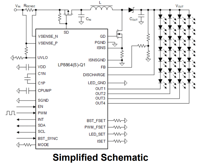
Detailed Description
Okay, so the LP8864-Q1 is this high-efficiency LED driver that is perfect for automotive stuff. We are talking things like those fancy infotainment displays, the instrument clusters in your car, and even heads-up displays (HUDs), plus other LED backlighting systems.
Basically if it is lighting up something in your car, this chip might be behind it.
Now by default you can control how bright the LEDs are using a PWM input which is pretty standard. But get this, you can also tweak the brightness through the I2C interface which gives you some extra flexibility.
For setting things up we have these external resistors that you connect to specific pins—BST_FSET, PWM_FSET, and ISET. These resistors let you set key parameters like the boost frequency, the LED PWM frequency and how much current is going to those LED strings.
Also there is this INT pin that is like a fault reporter. If something goes wrong it will let you know and you can clear the status either through the I2C interface or automatically when the EN pin goes low.
This chip is all about that pure PWM dimming and has six LED current drivers, each pushing up to 200mA. But here is where it gets versatile, you can gang those outputs together if you need to drive higher-current LEDs.
The ISET resistor sets the maximum LED driver current and you can fine-tune it even further using the I2C-controlled LEDx_CURRENT[11:0] register.
The PWM_FSET resistor is what you use to set the LED output PWM frequency while the LED_SET resistor tells you how many LED strings are active. Depending on how you set it up, the device automatically adjusts the phase shift.
For example if you are in a four-string mode, each output gets phase-shifted by 90 degrees (360°/4). And do not forget, any outputs you are not using need to be tied to GND which disables them and makes sure they do not mess with the adaptive voltage control or cause any false LED fault alerts.
To keep everything running efficiently, there is a resistor divider between VOUT and the FB pin that sets the maximum boost voltage.
The cool part is that the device constantly watches the voltages of the active LED strings and adjusts the boost voltage to the lowest level it needs. You can set the boost switching frequency anywhere from 100kHz to 2.2MHz using the BST_FSET resistor.
Plus it has a soft-start feature to keep the current draw from your power supply low when it is starting up. And it can even handle an external power-line FET to stop battery leakage when it is off while also giving you some isolation and fault protection.
The LP8864-Q1 is a remarkable device which comes loaded with many fault detection capabilities when it comes to ensuring system reliability and protection. Let us get into the details of what makes this driver so robust!
Comprehensive Fault Detection Features:
Detection of Open or Shorted LED Strings: This feature is crucial, because it identifies any faults in the LED strings preventing excessive heating that could occur if there is an open or short circuit. This means that we can keep our systems safe from potential damage due to faulty LEDs.
Detection of LEDs Shorted to Ground: The LP8864-Q1 monitors for situations where LEDs might inadvertently short to ground which is another layer of safety we can rely on.
Monitoring of External Resistor Values: It keeps an eye on the external resistors connected to various pins like ISET, BST_FSET, PWM_FSET, LED_SET, and MODE. If any resistor goes out of range we will be notified allowing us to take corrective action before any issues escalate.
Boost Circuit Protection: This feature safeguards against overcurrent and overvoltage conditions in the boost converter ensuring that our circuits operate within safe limits.
Undervoltage Protection for the Device (VDD UVLO): The LP8864-Q1 continuously monitors the voltage at the VDD pin. If it detects low voltage conditions we can prevent malfunctioning before it even starts.
Overvoltage Protection for the VIN Input (VIN OVP): It senses excessive voltage at the VSENSE_P pin, which helps protect our device from potential damage due to high voltage spikes.
Undervoltage Protection for the VIN Input (VIN UVLO): Similar to its VDD counterpart, this feature detects low voltage conditions via the UVLO pin, adding an extra layer of security for our input power.
Overcurrent Protection for the VIN Input (VIN OCP): By monitoring the voltage difference between the VSENSE_P and VSENSE_N pins it helps us to detect excessive current draw which is crucial for maintaining operational integrity.
Main Features
Control Interface:
EN (Enable Input): Think of this as the on/off switch for the LP8864-Q1. When the voltage at the EN pin goes above a certain point (VENIH), then the device powers up. When it drops below another point (VENIL), it shuts down. When it is on then all the internal stuff starts working.
PWM (Pulse Width Modulation): This is the default way we control the brightness of the LED current sinks. Basically it adjusts the duty cycle to dim or brighten the LEDs.
INT (Interrupt): This is like a fault alarm. It is an open-drain output that tells us when something goes wrong.
SDA and SCL (I2C Interface): These are the data and clock lines for the I2C interface. We use these to control the brightness of the current sinks and to read back any fault conditions for diagnostics.
BST_SYNC: This pin is for the boost converter's switching frequency. You can feed it an external clock signal to control the boost clock mode.
The device automatically detects an external clock at startup. If there is no external clock then it uses its own internal clock.
You can also tie this pin to VDD to enable a boost spread spectrum function or tie it to GND to disable it.
ISET pin: We use this to set the maximum current level for each LED string.
Function Setting:
BST_FSET pin: Use this to set the boost switching frequency by connecting a resistor between this pin and ground.
PWM_FSET pin: This sets the LED output PWM dimming frequency using a resistor to ground.
MODE pin: This pin sets the dimming mode using an external resistor to ground.
LED_SET pin: Use this to configure the LED setup with a resistor to ground.
ISET pin: This sets the maximum LED current level per OUTx pin.
Device Supply (VDD):
The VDD pin supplies power to all the internal parts of the LP8864-Q1. You can use either a 5V or 3.3V supply, typically from a linear regulator or a DC/DC converter, making sure it can handle at least 200mA of current.
Enable (EN):
The LP8864-Q1 only activates when the voltage at the EN pin is above a certain threshold (VENIH) and deactivates when the voltage drops below another threshold (VENIL).
All the analog and digital components become active once the LP8864-Q1 is enabled via the EN pin. If the EN pin is not active then the I2C interface and fault detection will not work.
Charge Pump
Now let us check how we can manage the charge pump situation in our setup. Basically we have got an integrated regulated charge pump that can be a real asset for supplying the gate drive for the external FET of the boost controller. Here is the scoop:
So the cool thing is that this charge pump can be enabled or disabled automatically. It figures out whether VDD and the CPUMP pin are connected together. If the voltage at VDD is less than 4.5V then the charge pump kicks in to generate a 5V gate voltage. This is what we need to drive that external boost switching FET.
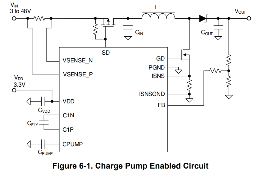
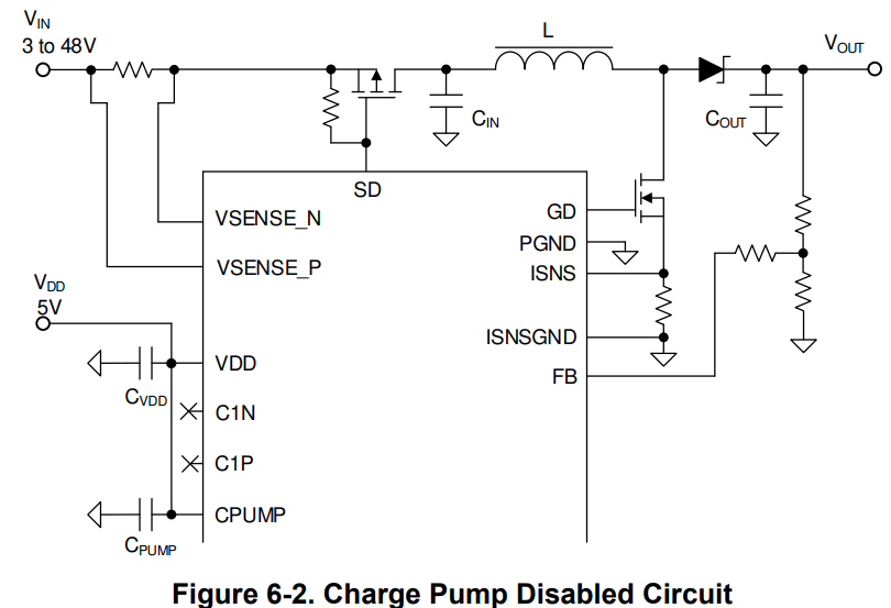
Now if we are going to use the charge pump then we will need to pop a 2.2µF capacitor between the C1N and C1P pins. This helps it do its thing.
On the flip side if we do not need the charge pump then no worries! We can leave the C1N and C1P pins unconnected. Just remember to tie the CPUMP pins to VDD.
Regardless of whether we are using the charge pump or not we need a 4.7µF CPUMP capacitor which stores energy for the gate driver. It is super important that this CPUMP capacitor is used in both scenarios (charge pump enabled or disabled) and we want to place it as close as humanly possible to the CPUMP pins.
Basically if the charge pump is enabled then we have a couple of status bits that can give us some useful info.
First up we have the CPCAP_STATUS bit. This guy tells us whether a fly capacitor was detected. It is like a little confirmation that everything is connected correctly.
Next theres the CP_STATUS bit. This one shows us the status of any charge pump faults. If anything goes wrong with the charge pump, this bit will let us know. And it also generates an INT signal which is like an alert that something needs our attention.
Now here is a handy feature: if we do not want the charge-pump fault to cause an interrupt on the INT pin then we can use the CP_INT_EN bit to prevent it. This can be useful if we want to handle the fault in a different way or if we do not want to be constantly interrupted by it.
Boost Converter Stage
so basically we are talking about a boost controller which is like a step-up device for voltage in circuits. Specifically the LP8864-Q1 uses current-mode control to handle this boost DC/DC conversion which is how we get the right voltage for the LEDs.
The boost concept works using a current-mode-controlled topology and it has this cycle-by-cycle current limit thing going on. It keeps an eye on the current using a sense resistor that is hooked up between ISNS and ISNSGND.
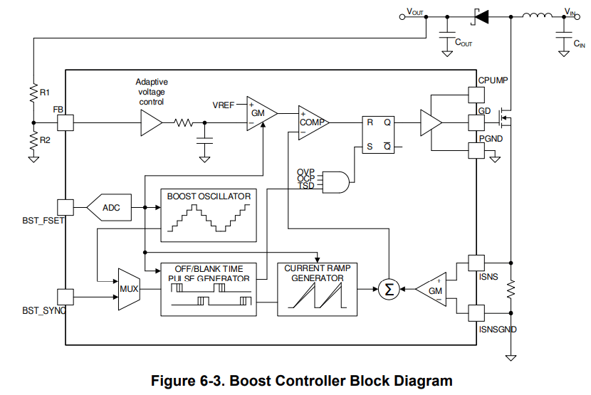
If we use a 20mΩ sense resistor then we are looking at a 10A cycle-by-cycle current limit. Depending on what we are doing, that sense resistor could be anywhere from 15mΩ to 50mΩ.
Also we can set the maximum boost voltage using an external FB-pin resistor divider that is connected between VOUT and FB.
At BST_FSET, an external resistor allows the boost switching frequency to be adjusted between 100kHz and 2.2MHz, as given in the following table. A 1% accurate resistor is required to guarantee correct functioning.
| R_BST_FSET (kΩ) | BOOST FREQUENCY (kHz) |
|---|---|
| 3.92 | 400 |
| 4.75 | 200 |
| 5.76 | 303 |
| 7.87 | 100 |
| 11 | 500 |
| 17.8 | 1818 |
| 42.2 | 2000 |
| 124 | 2222 |
Boost Cycle-by-Cycle Current Limit
The voltage that exists between ISNS and ISNSGND plays a crucial role here because it is utilized for both the current sensing of the boost DC/DC controller and the settings for the cycle-by-cycle current limit.
Now when we hit that cycle-by-cycle current limit the controller will immediately turn off the switching MOSFET. Then in the next switching cycle it will turn it back on again. This mechanism acts as a common safeguard for all related DC/DC components such as inductor, Schottky diode, and switching MOSFET, ensuring that the current does not go beyond their maximum limits.
And this cycle-by-cycle current limit is not going to give rise to any faults in the device.
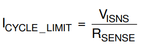
where, VISNS = 200mV
Controller Min On/Off Duration
The table below shows the shortest possible on/off time for the device boost DC/DC controller. System layout must give particular attention to the minimum off time. The increasing and decreasing times of the SW node are supposed to be greater than the minimum off period to prevent the MOSFET from not being turned off by the controller.

Boost Adaptive Voltage Control
Boost Adaptive Voltage Control with the LP8864-Q1 boost DC/DC converter is responsible for generating the anode voltage for our LEDs. When everything is running smoothly then the boost output voltage adjusts itself automatically according to the LED current sink headroom voltages. This useful feature is known as adaptive boost control.
To set the number of LED outputs we want to use we simply utilize the LED_SET pin. Only the active LED outputs are monitored to manage this adaptive boost voltage. If any LED strings encounter open or short faults then they are promptly excluded from the adaptive voltage control loop ensuring that we maintain optimal performance.
The control loop keeps a close eye on the LED driver pin voltages and if any of the LED outputs dip below the VHEADROOM threshold then it raises the boost voltage. Conversely if any of those outputs reach the VHEADROOM threshold then the boost voltage is lowered accordingly. For a visual representation of how this automatic scaling works based on the OUTx-pin voltage, VHEADROOM, and VHEADROOM_HYS, we can refer to Figure below.
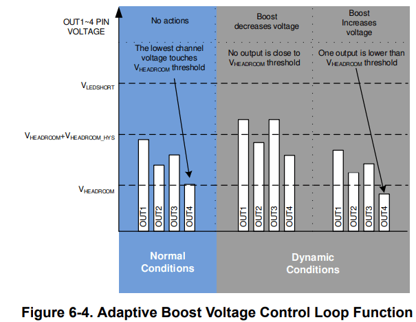
The resistive divider composed of R1 and R2 plays a crucial role by defining both the minimum and maximum levels for adaptive boost voltage. Interestingly the feedback circuit operates consistently in both boost and SEPIC topologies. When we choose our maximum boost voltage then it is essential to base that decision on the maximum LED string voltage specification; we need at least 1V higher than this maximum to ensure that our current sink functions correctly.
Before activating the LED drivers we initiate a startup phase where the boost reaches its initial level—approximately at 88% of the range between minimum and maximum boost voltages. Once our LED driver channels are up and running, then boost output voltage continues to adjust automatically based on OUTx pin voltages.
Additionally the FB pin resistor divider is instrumental in scaling not just the boost overvoltage protection (OVP) and overcurrent protection (OCP) levels but also manages short-circuit levels in applications like HUDs.
FB Divider Employing the Two-Resistor Technique
The boost output voltage and ground are connected via a two-resistor divider circuit in a standard FB-pin configuration.
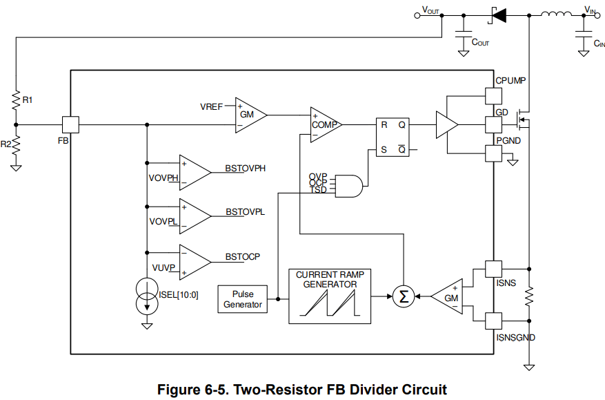
The Equation below may be used to compute the highest boost voltage. When entire LED strings remain unplugged or while performing OPEN string detection, the maximum boost voltage can be achieved.
VBOOST_MAX = ISEL_MAX × R1 + ((R1 / R2) + 1) × VREF
where
- VREF = 1.21V
- ISEL_MAX = 38.7µA
- R1 / R2 normal recommended range is 7~15
The minimum LED string voltage must be greater than the minimum boost voltage. This equation is used to determine the minimum boost voltage:
VBOOST_MIN = ((R1 / R2) + 1) × VREF
where
- VREF = 1.21V
The boost controller stops switching the boost FET and sets the BSTOVPL_STATUS bit when the boost OVP_LOW level is achieved. Throughout this state, the LED drivers remain operational, and when the boost output level drops, the boost switches back to its regular mode. The present boost voltage causes a dynamic shift in the boost OVP low voltage threshold. Equation below can be utilized for calculating it:
VBOOST_OVPL = VBOOST + ((R1 / R2) + 1) × (VFB_OVPL - VREF)
where
- VFB_OVPL = 1.423V
- VREF = 1.21V
The boost controller switches to fault recovery mode and sets the BSTOVPH_STATUS bit once the boost OVP_HIGH level is achieved. The following equation is used to determine the boost OVP high-voltage threshold, which likewise varies dynamically with current boost voltage:
VBOOST_OVPH = VBOOST + ((R1 / R2) + 1) × (VFB_OVPH - VREF)
where
- VFB_OVPH = 1.76V
- VREF = 1.21V
The boost controller initiates a 110ms OCP counter as soon as the boost UVP threshold is achieved. In the event the boost voltage remains below the UVP threshold before the timer goes off, the LP8864-Q1 device switches to fault recovery mode and adjusts the BSTOCP_STATUS bit.
Equation below computes the boost UVP voltage threshold, which likewise varies dynamically with the currently applied boost voltage:
VBOOST_UVP = VBOOST - ((R1 / R2) + 1) × (VREF - VUVP)
where
- VUVP = 0.886V
- VREF = 1.21V
Implementing the Three-Resistor Approach for a Two-FB Divider
Applications requiring less than 200kΩ resistors can make use of an FB-pin circuit with a three-resistor divider circuit.
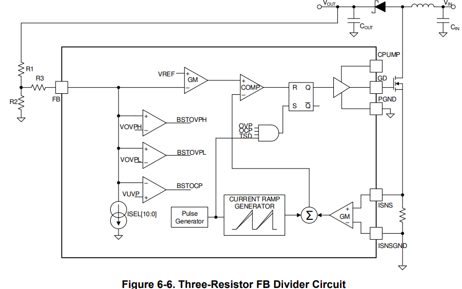
The Equation below may be used to compute the maximum boost voltage. When each and every LED strings are left unplugged or while performing OPEN string detection, the maximum boost voltage can be achieved.
V_BOOST_MAX = ( (R1 * R3) / R2 + R1 + R3 ) * I_SEL_MAX + ( (R1 / R2) + 1 ) * V_REF
where:
- V_REF = 1.21V
- I_SEL_MAX = 38.7μA
- R1 / R2 normal recommended range is 7 to 15
The minimum boost voltage must be less than the minimum LED string voltage.
The minimum boost voltage is calculated as:
V_BOOST_MIN = ( (R1 / R2) + 1 ) * V_REF
Upon reaching the boost OVP_LOW level, the boost controller sets the BSTOVPL_STATUS bit and ceases switching the boost FET. While this state, the LED drivers remain operational, and when the boost output level drops, the boost switches back to its regular mode.
The boost OVP low voltage threshold is calculated as follows and varies dynamically with the current boost voltage:
Equation for V_BOOST_OVPL:
V_BOOST_OVPL = V_BOOST + ((R1 / R2) + 1) * (V_FB_OVPL - V_REF)
where:
- V_FB_OVPL = 1.423V
- V_REF = 1.21V
Upon reaching the boost OVP_LOW level, the boost controller switches to fault recovery mode, setting the BSTOVPH_STATUS bit.
Calculated using Equation 10, the boost OVP high-voltage threshold also varies dynamically with the present boost voltage.
Equation for V_BOOST_OVPH:
V_BOOST_OVPH = V_BOOST + ((R1 / R2) + 1) * (V_FB_OVPH - V_REF)
where:
- V_FB_OVPH = 1.76V
- V_REF = 1.21V
The boost controller initiates a 110ms OCP counter as soon as the boost UVP level is achieved. In the event the boost voltage falls below the UVP limit before the timer goes off, the LP8864-Q1 device switches to fault recovery mode and sets the BSTOCP_STATUS bit.
The following Equation is used to determine the boost UVP voltage threshold, which also varies dynamically with the present boost voltage.
Equation for V_BOOST_UVP:
V_BOOST_UVP = V_BOOST - ((R1 / R2) + 1) * (V_REF - V_UVP)
where:
- V_UVP = 0.886V
- V_REF = 1.21V
Using External Compensation for FB Divider
In the majority of circumstances, the device's internal compensation network maintains a stable DC-DC control loop.
To provide greater versatility in loop design or to address specific exceptional use-cases, a separate external compensation network might be connected to FB-pin.
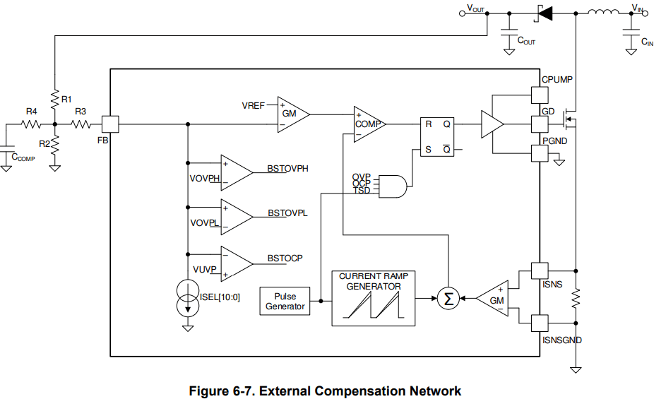
One more pole and one more zero will be added to the loop by this network.
f_POLE_COMP = 1 / (2π * [(R1 || R2) + R4] * C_COMP)
f_ZERO_COMP = 1 / (2π * R4 * C_COMP)
It should be mentioned that R3 is not involved in the compensation. Therefore, there is no need to modify the equation when using this external compensation network in a T-divider network or a two-divider network.
For instance, adding a pole at 1 kHz and a zero at 2 kHz can reduce the loop gain by around 6 dB beyond 2 kHz in real-world applications where stability issues arise in DC-DC loops. Gain margin and phase margin are both going to benefit from this.
Boost Sync and Spread Spectrum
When the BST_SYNC pin is high, the spread spectrum function may be activated; once it is low, it may be deactivated.
An external CLK signal on the BST_SYNC pin could be used to clock the boost controller. The spread spectrum function will be activated or disabled based on the final pin level of BST_SYNC, and the boost will keep on running at the frequency specified by the RBST_FSET resistor should the clock go away later.
| BST_SYNC PIN LEVEL | BOOST CLOCK MODE |
|---|---|
| Low (GND) | Spread spectrum disabled |
| High (VDDIO) | Spread spectrum enabled |
| 100kHz to 2222kHz clock frequency | Spread spectrum disabled, external synchronization mode |
The RBST_SET resistor must be selected based on the boost frequency possibilities that are nearest to the external frequency when utilizing the external BST_SYNC input.
EMI noise surrounding the switching frequency is reduced by the spread spectrum function, and its harmonic levels. The internal spread spectrum function uses a modulation frequency of 200 Hz to 1.2 kHz to modify the boost frequency ±3.3% to 7.2% from the core frequency.
The SPREAD_RANGE and SPREAD_MOD_FREQ registers can be used to program the modulation frequency and the switching frequency deviations, respectively. Using an external synchronization clock prevents the spread-spectrum function from working.
Table 6-4. Spread Spectrum Frequency Range
| SPREAD_RANGE Binary Value | Switching Frequency Variation |
|---|---|
| 00 | ±3.3% |
| 01 | ±4.3% |
| 10 (Default) | ±5.3% |
| 11 | ±7.2% |
Table 6-5. Spread Spectrum Modulation Frequency
| SPREAD_MOD_FREQ Binary Value | Modulation Frequency |
|---|---|
| 00 (Default) | 200Hz |
| 01 | 500Hz |
| 10 | 800Hz |
| 11 | 1200Hz |
Boost Output Discharge
When we say that EN pin low, then here is what happens in a nutshell.
First we are stopping the boost controller and those LED current sinks dead in their tracks. Think of it like hitting the brakes on everything.
Next we are turning off the power-line FET.
After that we are starting to discharge the boost output. The discharge pin usually sucks about 30mA of current. The DISCHARGE pin must be connected with boost output for normal operation.
This discharge lasts for about 400ms. After that the whole thing shuts down.
Now there is an internal comparator keeping an eye on the DISCHARGE pin's voltage. If that voltage goes above VBST_OVPH – usually around 50V – then the device enters fault recovery mode and reports a BST_OVPH fault. This is a safety net in case the boost voltage goes totally bonkers because of some system meltdown.
Just a heads up: This discharge function is only available if we are using the HTSSOP package, then. If you are rocking the QFN package, then we do not have this function.
Light Load Mode
Our DC-DC controller will go into light load mode if:
The VIN voltage is super close to the VOUT voltage, then.
The loading current is barely there, then.
The PWM pulse width is really, really short, then.
When the DC-DC converter goes into light load mode then it will stop switching here and there to make sure the output voltage does not climb too high. You might also hear this called PFM mode since the DC-DC converter's switching frequency is going to be all over the place in this mode.
For more explanation on this subject you can refer to the following pdf:
LP8864-Q1 Automotive Display LED-backlight Driver with Four 200mA Channels
Need Help? Please Leave a Comment! We value your input—Kindly keep it relevant to the above topic!