A bipolar transistor or a BJT is a 3 terminal semiconductor device which is able to amplify or switch small signal input voltages and currents to significantly larger output signal voltages and currents.
How Bipolar Junction Transistor BJTs Evolved
During 1904–1947, the vacuum tube was unquestionably the electronic device of great curiosity and growth. In 1904, the vacuum-tube diode was launched by J. A. Fleming. Soon afterwards, in 1906, Lee De Forest enhanced the device with a third feature, known as the control grid, producing the first amplifier, and named as the triode.
In the subsequent decades, radio and television induced huge inspiration to the tube business. Manufacturing went up from around 1 million tubes in 1922 to around 100 million in 1937. In the beginning of 1930s the 4 element tetrode and 5 element pentode acquired popularity in the electron-tube business.
In the years that would follow, the manufacturing sector evolved into one of most important sectors, and speedy improvements were created for these models, in the production methods, in high-power and high-frequency applications, and in the direction of miniaturization.
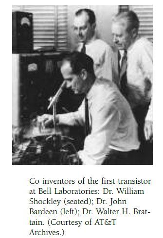
On December 23, 1947, however, the electronics industry was going witness the arrival of an absolutely brand new "direction of interest" and improvement. It turned out on the mid-day that Walter H. Brattain and John Bardeen exhibited and proved the amplifying function of the very first transistor at the Bell Telephone Laboratories.
The very first transistor (which was in the form of a point-contact transistor) is demonstrated in Fig. 3.1.
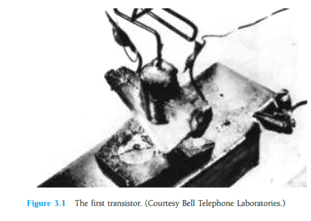
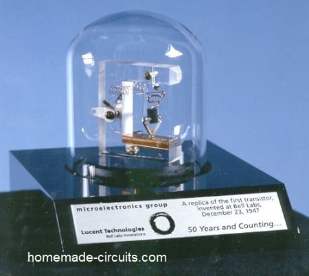
Image Courtesy: https://commons.wikimedia.org/wiki/File:Replica-of-first-transistor.jpg
The positive aspects of this 3 pin solid-state unit in contrast to the tube were instantly noticeable: It turned out to be much smaller, could work without an "heater" or heating losses, was unbreakable and strong, was more efficient in terms of power usage, could be stored and accessed with ease, didn't require any initial warming start up, and it worked at much lower operating voltages.
TRANSISTOR CONSTRUCTION
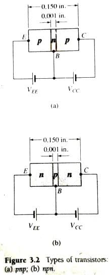
A transistor is basically a device built with 3 layer of semiconductor material in which either 2 n- type and a single p- type layer of material is used or 2 p- type and a single n- type layer of material is used. The first type is called an NPN transistor, while the second variant is named as the PNP type of transistor.
Both of these types could be visualized in the figure 3.2 with appropriate DC biasing.
We have already learned how in BJTs DC biasing become essential for establishing the required operational region and for AC amplification. For this the emitter side layer is doped more significantly compared to the base side which is doped less significantly.
The outer layers are created with layers much greater in thickness compared to the p- or n- type sandwiched materials. In Fig 3.2 above, we can find that for this type the proportion of the total width in comparison to the central layer is around 0.150/0.001 : 150:1. The doping implemented over the sandwiched layer is also relatively lower than the outside layers which ranges typically across 10 : 1 or even lesser.
This kind of reduced doping level lowers the conduction capacity of the material and increases the resistive nature by restricting the quantity of the free moving electrons or the "free" carriers.
In the biasing diagram we can also see that the terminals of the device are shown using capital letters E for emitter, C for collector and B for base, in our future discussion I'll explains the why this importance is rendered to these terminals.
Also, the term BJT is used for abbreviating bipolar transistor and designated to these 3 terminal devices. The phrase "bipolar" indicate the relevance of the holes and electrons involved during the doping process with respect to an oppositely polarized substance.
TRANSISTOR OPERATION
Let's now understand the fundamental working of a BJT with the help of an PNP version of the Fig 3.2. The operating principle of an NPN counterpart would be exactly similar if the participation of the electrons and the holes are simply interchanged.
As can be seen in Figure 3.3, the PNP transistor has been redrawn, eliminating the base to collector biasing. We can visualize how the depletion region looks narrowed in width due to the induced biasing, which causes a massive flow of the majority carriers across p- to the n- type materials.
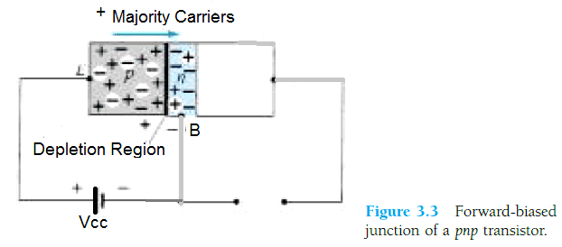
In case the base-to-emitter bias of the pnp transistor is removed as demonstrated in Fig 3.4, the flow of the majority carriers becomes zero, allowing the flow of only minority carriers.
Briefly we can understand that, in a biased situation one p-n junction of a BJT becomes reverse biased while the other junction is forward biased.
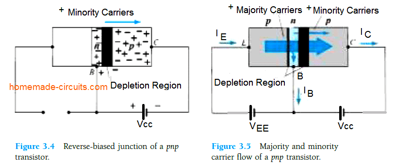
In Fig. 3.5 we can see both biasing voltages being applied to a pnp bipolar transistor, which causes the indicated majority- and minority-carrier flow. Here, from the widths of the depletion regions we can clearly visualize which junction has working with a forward-biased condition and which is in reverse-biased.
As shown in the figure a substantial quantity of majority carriers end up being diffused across the forward-biased p-n junction into the n-type material. This raises a question in our minds, could these carriers play any important role to promote the base current IB or enable it to flow directly into the p-type material?
Considering that the sandwiched n-type content is incredibly thin and possesses minimal conductivity, an exceptionally few of these carriers is going to take this particular route of high resistance across the base terminal.
The level of the base current is normally around microamperes rather than milliamperes for the emitter and collector currents.
The bigger range of these majority carriers are going to diffuse along the reverse-biased junction into the p type material attached to the collector terminal as pointed out in Fig. 3.5.
The actual cause behind this relative ease with which the majority carriers are allowed to get across the reverse-biased junction is quickly realized by the example of a reverse biased diode where the induced majority carriers turn up as minority carriers in the n-type material.
To put it differently, we find an introduction of minority carriers into the n-type base region material. With this knowledge and along with the fact that for diodes all the minority carriers in the depletion region get across the reverse-biased junction, results in the flow of electrons, as indicated in Fig. 3.5.
Assuming the transistor in Fig.3.5 to be a single node, we can apply Kirchhoff's current law to get the following equation:
IE = IC + IB
Which shows that the emitter current is equal to the sum of base and collector current.
However, the collector current is made up of a couple of elements, which are namely the majority and the minority carriers as proven in Fig.3.5.
The minority-current carrier element here constitutes the leakage current, and is symbolized as ICO (current IC having an open emitter terminal).
Consequently, the net collector current is established as given in the following equation 3.2:
IC = ICmajority + ICOminority
Collector current IC is measured in mA for all general purpose transistors, while ICO is calculated in uA or nA.
ICO will behave quite like a reverse biased diode and therefore could be vulnerable to temperature changes, and therefore must be appropriately taken care while testing, especially in circuits which are designed to work in widely varying temperature range scenarios, or else the result can be hugely affected due to the temperature factor.
That said, due to the many advanced enhancements in the construction layout of the modern bipolar transistors, the ICO is significantly reduced and can be completely ignored for all today's BJTs.
In the next chapter I have explained how to configure BJTs in the common base mode.
References: https://en.wikipedia.org/wiki/John_Bardeen
Dear Swagatham, thanks for the reply.
So, that means MJE13005 (Vce-400VDC) can be used in low voltage DC (5V,12V, 24V etc…etc..) circuits also. Is it correct what I did understand….?
Regards
Hi Anil, yes they can be used as long as the working current range is within the transistor’s limit.
Hi dear Swagatham
I have few working MJE13005 transistors from CFLs. As per datasheet, these are 400V, 4A, NPN transistors. I hve never seen this transistors in any other circuits, except CFL,s, Electronic ballasts and SMPS’s.
So, my question:-
Can we use these tranistors as general purpose transistors like eg. TIP122 for driving small dc motors, switching ON/OFF high wattage LEDs (within its 4A Ic spec.)….etc…etc… .
If I ask more simply, can I replace a TIP122 in a 10watt LED PWM control circuit with MJE13005. (Power supply is 12V, 3A.) Here TIP122 is the output transistor which drives the load 10W LED
Thanks in advance.
Dear Anil,
Yes it will work, but TIP122 being a Darlington type has a high gain. To get the same gain you may have to add a 2N2222 NPN with MJE13005 for optimal results.
hello dear sir
my name is bruce i have been fallowing your blog for a long time it has been fun to watch your site evolve
i have built many of your circuits thank-you!!!
i need tour help with a battery charger design my father(94) has a scooter and the charger died
it uses 2 35ahr sealed lead-acid batteries 12v there is a three pin connector for the charger
one wire goes to battery 1 pos another to battery 2 neg the goes to where the two are connected in series
i think that configuration is to charge the two batteries individually
thanks to your blog i have designed many specialty chargers but need your help on this one thanks again!
Thank you Bruce, yes you can charge them individually using a DC power supply regulated at around 14V, and having a current rating of less than 5 amps. You can connect a voltmeter across the battery to check when it reaches 14V, and then switch OFF the power supply. This is simplest way to get your battery charge safely.