Boolean algebra is a assortment of basic mathematical techniques applied to signify and communicate the logical procedures that happen within a digital circuit.
Difference Between Boolean Algebra and Common Algebra
Boolean algebra is much like common algebra.
The main distinction is that in contrast to common algebra, in which we have parameters that can be of any magnitude, in Boolean algebra only the values 0 and 1 are accepted.
Apart from this, almost all of the fundamental operating rules that are used in common algebraic expressions are used in Boolean logic also.
Advantages of Boolean Algebra
The best advantage of Boolean algebra is that it gives a solution to express digital-logic procedures mathematically.
Boolean equations could be put forth to accurately explain exactly how a logic circuit works, so that you are able to design this kind of circuits.
Boolean algebra additionally offers a method to reduce the quantity of gates that may be required for a logic circuit and thus simplifies the circuit design a lot. This enables the users to decrease the all round cost of the logic design, and help minimize power consumption.
Furthermore, the boolean equations are able to quickly demonstrate exactly what is happening in a logic circuit to help you find the possible faults.
Remember not to get afraid of the terms like "Boolean," "equation," "mathematical expression," or "algebra" when you start understanding the vocabulary and also the number of basic principles introduced here.
Even complicated circuits can start appearing simple for you.
Hence, prepare for a digital logic tutorial, after that we are going to enjoy composing the Boolean equations of a circuit and developing a circuit from those equations.
Reviewing Digital-Logic Circuits.
In the past, you might have figured out exactly how fundamental logic circuits work. You can go through the following articles which have extensively discussed regarding the working of the various logic circuits. Once you refresh with the logical diagrams, truth tables and the working procedures of the logical gates, you can come back here to leran the boolean algebra principles involved with these gates.
Expressing Logic Mathematically
To start applying Boolean algebra, we must obtain some method to show the basic logic procedures implementing mathematical expressions. Let's check out the options for conveying inversion, AND, OR , NAND, and NOR functions.
While you understand the fundamental rules, remember that the binary signals that are being processed by the logic circuits are referred to as variables.
- Variables are signals that will change value.
- Binary variables may have any two of the values, either a 1 or a 0 value.
- Variables are generally offered names to differentiate them from each other.
- Alphabetical letters are the most popular method used to distinguish between the variables, though several additional alpha or alphanumeric titles can also be applied.
- Generally signals are provided some variable name (mnemonic) which is merely a short-cut technique of referring to the signal.
- A good example is a binary signal known as "clear," which can be symbolized by the mnemonic CLR.
- Frequently you will find binary signals are arranged collectively and related as in a binary number.
- For instance, the bits in an 8-bit word could be offered the names A0 through A7. Whatever may be the case, you may come across numerous variations.
Inversion
Inversion is mathematically indicated by putting a bar on top of the variable. As shown in the Fig. 1, the inverter input is A while the output is B. Observe that B is portrayed in terms of A.
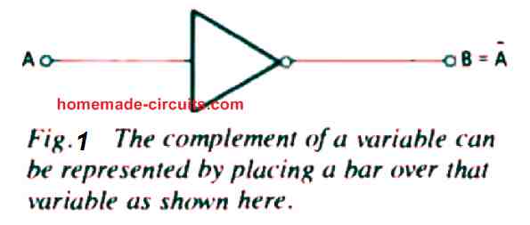
This expression is stated as B is equal to NOT A. The NOT bar shows that signal A has become inverted. Keep in mind that A could be either a binary 0 or a binary 1. NOT A, needless to say, will be the opposite, or complementary to the NOT B.
Considering that it is not easy to write a bar on top of the letter as demonstrated in Fig. 1, some other easier techniques happen to be created for symbolizing inversion. Occasionally the inverted variable is mentioned by an asterisk or a prime (just like an accent).
Applying the variables in Fig. 1 we get the following equation:
B= A * or B =A'
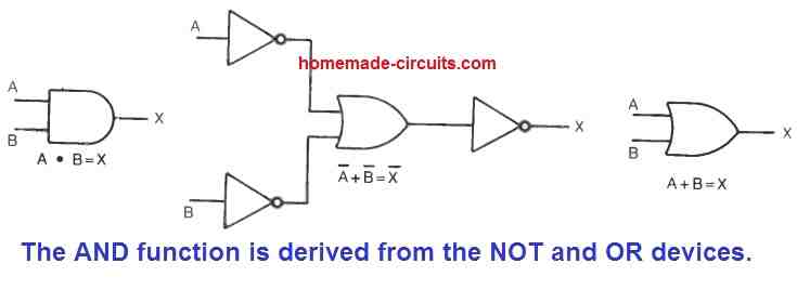
AND Function
The logical AND functioning is expressed by putting a dot between the two variables to make it ANDed. This is highlighted in Fig. 2.
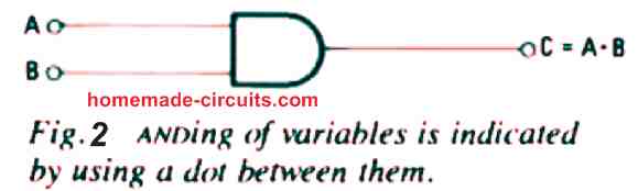
The a pair of inputs to the AND gate are A and B and the output is specified as C.
Understand this manifestation for the output:
C = AB
In normal algebra AB might suggest multiply A and B together. For this reason the output of an AND gate is normally referred to as product of the inputs.
Like in standard algebra, it isn't essential to indicate any symbolic representation between a pair of variables (despite the fact that at times a dot can be used). As an alternative, the letters are simply put next to one another.
Figure 3 exhibits a four-input AND gate having different input variables. Frequently you might notice the output equation expressed using certain variables split up by parentheses.
Every input expression presents itself inside a pair of parentheses to help keep these visually segregated in order to avoid confusion.
However given each of these terms are written immediately next to one another, it indicates that the variables are ANDed with each other.
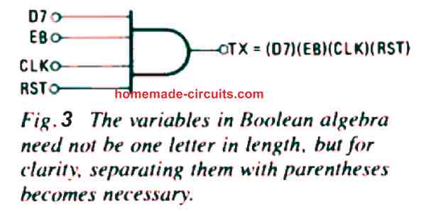
In Fig. 3, we state that the output product is:
TX = (D7)(EB)(CLK)(RST)
OR Function
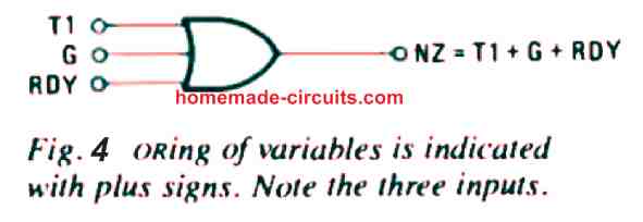
The logical gate OR is displayed by inserting a + symbol between variables. This is highlighted using the three-input OR gate as demonstrated in Fig. 4. Commonly you might discover the output of an OR gate being called as the sum of the input variables.
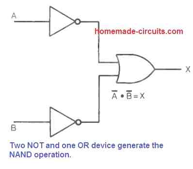
NAND Function
The NAND or NOT-AND functionality is just the inverted product of the input variables. A good example is demonstrated in Fig. 5. The output term is expressed just as it might be done for an AND gate, except by presenting a NOT to the complete expression.
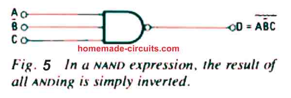
This may be carried out by inserting a bar on top of the whole expression as found in Fig. 5. For expressing in an alternate way, the ANDed input terms could be placed into parentheses and an asterisk or apostrophe applied to suggest the NOT function. Observe that the term B includes a NOT bar on top of it.
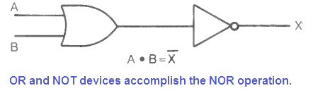
The NOR Function
In order to create the NOR logic function, we basically invert a fundamental OR output. Figure 6 exhibits a four-input NOR gate. The output term is created simply by composing the input variables split up by + signs. Subsequently, a bar is positioned on top of the whole expression in order to invert it.
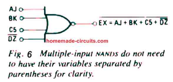
Once again remember that one term, DZ, is inverted at the input. Now, applying those basic (Boolean) expressions for every single logic gates, a lot more complex circuits could be quickly displayed.
Obtaining Boolean Expressions
Understanding the standard rules defined in the last paragraphs, we are now able to obtain a comprehensive Boolean expression for every larger, more advanced logic circuits.
The procedure is actually to get through the different logic gates beginning with the inputs, and creating the equation one step at a time. A few good illustrations can show you the method. Looking at the circuit in Fig. 7.
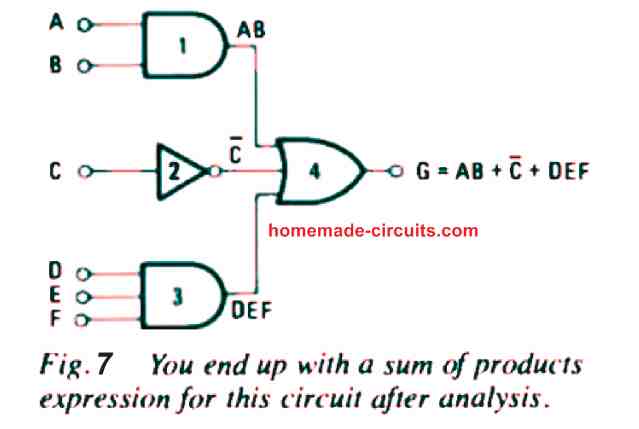
Observe that the input variables are marked. The output is specified as G.
The task is to produce the expression for G with regards to the input variables.
It's truly much less difficult than it actually appears to be.
To get started, you begin with the variables at the inputs which are all on the left hand side of the circuit. Write down their expression for each circuit's output.
For instance, the AND-gate 1 output is basically written as AB. The inverter 2 output is written as NOT C. The AND-gate 3 output is represented as DEF.
The outputs of gates 1 and 3, and inverter 2, constitute the inputs to OR-gate 4.
To finish the expression, we simply OR each of the inputs together with gate 4.
Subsequently, the output expression G turns into the following:
G = AB +C̅ +DEF
Check out the equation that we derived just above. You will usually notice an expression like this called a sum of products.
In our case, the products are classified as the ANDed variables AB and DEF. The sum, naturally, appertains to the ORing together of each of the products.
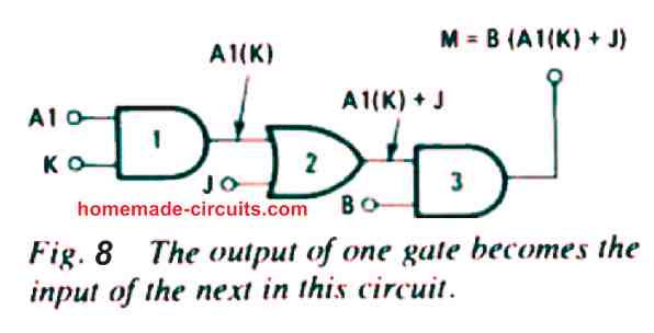
A little more advanced circuit is demonstrated in Fig.8. Even here the analysis procedure will be the exact same. Start working out from the circuit across left to right writing the output terms for each gate.
The gate 1 output will be A1(K) as displayed. We employ parentheses in cases like this to signify the separation amongst the a pair of variables, still they may be written next to each other to denote a product or AND function.
Next, the output of gate1 is ORed with the input of J. The causes the output from gate 2 to be:
A1(K) +J
This turns into one of the inputs to AND-gate 3. This expression is ANDed with input B to provide the finishing output expression:
M = B(A1(K) +J)
Yet again parentheses are employed here to separate the variables from each other and to guarantee that proper logical operation is depicted.
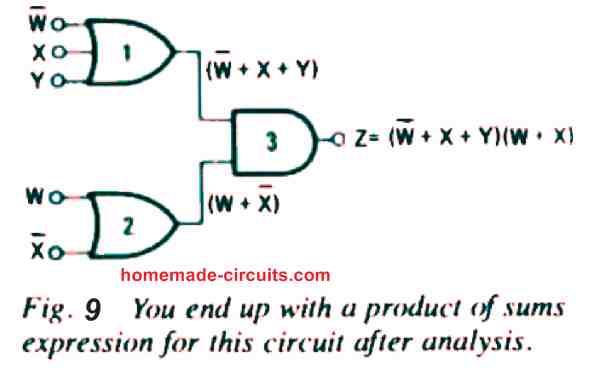
Examine the illustration in Fig.9. Once again, the method is to build the output expressions of the input gates, and then procedd through from left to right to generate the output. The output from gate1 will be:
( W̅ +X +Y)
The gate 2 output can be written as:
(W + X̅)
The a pair of outputs serve as the inputs to AND-gate 3. The final output expression is generated as, Z, simply by ANDing the two expressions with each other. We get the result as:
Z= (W̅ +X +Y)(W +X̅)
You may possibly come across this type of expression which is known as a product of sums.
Generating a Circuit From Equations
At this point we will think about the technique of sketching the logic circuit equivalent to a given Boolean expression. We will begin with the straightforward expression below:
W =XY +Z
The different logic functions suggested in the equation are quite simple to identify. The X and Y are put next to each other implying that the both signals are ANDed.
To indicate you just have to draw an AND gate using X and Y as being the inputs. The output of this AND gate XV will be ORed in the next step with an additional input called Z̅.
The + indication informs us we require an OR gate to accomplish this. If solely the variable Z is available, an inverter will be required to generate Z̅.
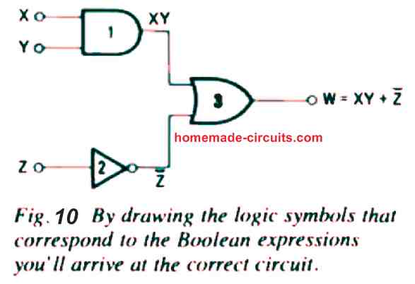
The circuit drawn accordingly can be witnessed in Fig. 10.
A rather more complicated illustration can be observed in the following equation:
X= (A +B +C)(D +E)(F)
The parenthesis let you know you have 3 distinct groups of variables ANDed together to create the output, X. The variables inside the groups are ORed with each other.
This could be started by making the circuits for each group of variables. The + sign within the parenthesis signify that an OR gate needs to be drawn. To begin with we can draw an OR gate having inputs A, B, and C̅.
An additional expression comes by ORing the input variables D̅ with E. Now draw an OR gate having the a pair of variables as its inputs.
The variable F within parenthesis will be ANDed along with the other pair of expressions.
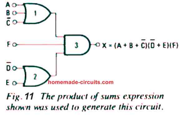
Lastly, to finish the circuit just draw an AND gate having 3 inputs and join these with the outputs of the a pair of OR gates and a signal input F as demonstrated in Fig. 11.
Summary
LOGIC functions can be represented in a variety of ways, including symbols, truth tables, and mathematics. The latter is called Boolean algebra, after George Boole, who invented the system of describing logic through a set of algebraic equations in the mid-nineteenth century.
Boolean algebra was viewed as an academic mathematical exercise until the introduction of the first electronic computers in 1938. It is now a tool used mostly by logic circuit designers.
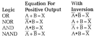
The following are the basic symbols used in Boolean algebra:
• for a series state or AND logic
+ for a parallel state or OR logic
- for inverted or the opposite state or NOT logic.
It's better to forget about traditional arithmetic at this point, where . equals multiply and + equals add; otherwise, Boolean algebra can be perplexing initially. As mentioned later, multiplication and addition are often used while dealing with Boolean algebra.
BASIC LOGIC
The figure below illustrates basic logic symbols with Boolean algebra equivalent equations.
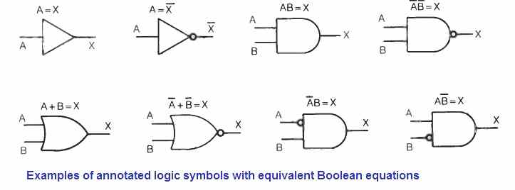
YES logic denotes a simple continuous condition, in which the output (X) equals the input (A). Obviously, the equivalent mathematical equation is A = X.
An inversion or opposite condition between input and output is represented by NOT logic. In this case the negation sign employed in the mathematical equation becomes A̅ = X (or A = X̅)
AND logic demands the presence of both inputs A and B before any output can be produced (a series condition), therefore the mathematical equation becomes A•B= X.
Since NAND logic is the inverse of AND logic, the equation becomes A̅•B̅ = X. This expression could also be written as A•B = X̅, which suggests the very same logic.
OR logic is a parallel condition in which an input should exist at either A or B before an output can be produced. The + symbol is used in this scenario, and the mathematical equation yields A + B = X.
Since NOR logic is the inverse of OR logic, the negative sign is introduced to produce A̅ + B̅ = X.
Only two inputs are specified in the above fundamental equations. Where there are additional inputs, the very same procedures apply. An AND gate with five inputs, for example, has the following equation:
A•B•C•D•E = X
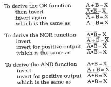
Each of the formulas for a logic function may be re-organized to produce the others, except the NOT (which possesses only one input, only to invert signals). While developing logic circuits, this feature becomes a valuable tool since it allows all essential functions to be depicted in the same logic, depending on the availability or preferences for certain components, i.e. all in OR logic, all in AND logic, or all in NAND logic.
This is generally accomplished by employing a NOT function (or one input NOR gate) as an inverter when desired, and following deMorgan's theorem, which asserts that inversion alters the state of the logic each time it is applied; that is, from • to + or + to • .
Starting with the AND function, for example:
A•B= X
Inversion flips the logic from AND (•) to OR (+):
A̅ + B̅ = X̅
Inverting the equation again yields a positive result:

which is equivalent to:
A+B = X
To put it another way, double inversion has turned an AND gate into an OR logic gate. The following figure depicts all of these stages.
The important thing to remember at this point is that inversion alters the sign of the equation as well as the input (except in a NOT gate). The following data illustrates this:
OR Logic
When using OR logic, equations must only employ the + sign, with inversion signals where necessary; that is, to turn a • sign to a + sign to produce the identical function, and to generate a positive output when needed.
The AND gate is used in the first example above to demonstrate how this is achieved.
In a similar fashion, NAND and NOR functionalities may be achieved.
The OR logic already includes the NAND function:
A̅ + B̅ = X
The inversion of both inputs is required when using an OR gate to produce a NAND function principle, as depicted in the following figure.
In AND logic, there is NOR function:
Since inversion on inversion returns the equation to its previous form, this formula may be reduced to:
A + B= X̅
In OR logic, the NOR function is thus implemented by an OR gate followed by a NOT gate for inversion. (See Figure below)
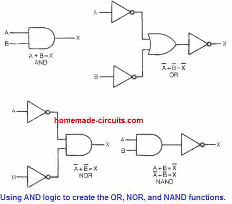
AND Logic
The goal here is to use the • (AND) symbol to denote all equations. An AND gate, of course, already performs this; A•B = X, as illustrated in the next figure below. Other logic functions that may be deduced from an AND gate are as follows:
The OR function could be achieved by inversion:
A̅ + B̅ = X̅
Inverting this again gives:

Which is actually the same as the following expression:
A+ B = X
AND logic already includes the NOR function (A̅•B̅ = X). The NAND function is essentially created by inverting the output of an AND gate A•B = X̅.
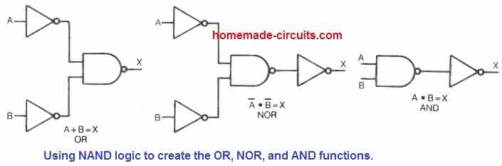
NAND Logic
The condition here is that all equations be written in the manner (inverted AND).
The figure below depicts the derivations of the OR, NOR, and AND functions.
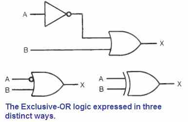
Exclusive OR
The previously discussed, OR gate produces an output if one or more inputs have a value of 1. It may be more precisely characterized as inclusive OR.
A two-input OR gate offers a potential version in which there is an output if one and only one of the inputs has a value of 1. This is referred to as the exclusive OR (often abbreviated XOR, and often referred to as non-equivalence) as depicted in the following figure.
It has a truth table, as illustrated in the image below.
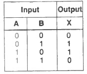
In other words, there is an output if A=1 or B=1, but not if both A=1 and B=1 occur at the same time. The related Boolean equation is as follows:
(A + B)(A̅B̅)= X
or AB̅ + A̅B = X
In this equation, observe that the period, or little point, between A and B has been removed. In reality, the point is practically seldom utilized and is believed to be present when two or more letters follow one another; meaning, when they sit next to one another.
A comparator or equality detector is one example of how an exclusive OR might be used. For example, there is an output, if there's a difference between the two input signals to the gate.
In this situation, the gate compares and identifies the difference between the two signals, in a way. The exclusive characteristic of the logic, on the other hand, indicates that there is no output if the two input signals are identical.
The lack of output implies that the inputs are equal.
Enable
Enable is an inhibit, as illustrated in the figure below, for a two-input AND gate with inhibit, which is given by a NOT applied to one input of an AND gate.
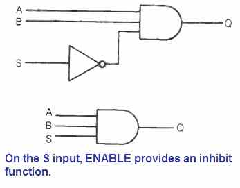
The strobe (S) or enable input is the third input, yielding in the truth table below, with Q as the output. When the strobe input is switched to high, the AND gate is set to low.
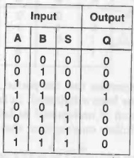
The AND gate produces a low at its output as a result of this. The AND gate's output is always low, regardless of what the other input receives.
As seen in the TABLE above, there is an output, 1, only when A = 1 and B = 1, and S = 0. The existence of an inhibit signal (S =1) maintains the output at 0 regardless of any potential combination of A and B, even if A =1, B = 1.
The corresponding Boolean equation is as follows:
ABS̅= Q
More on Boolean Algebra can be learned from the following pdf document:
https://www.homemade-circuits.com/wp-content/uploads/2021/05/boolean.pdf