

A anti-spy or bug detector circuit is a device that detects hidden wireless electronic devices such as wireless microphones, spy cameras, Wi-Fi devices, GPS trackers or any gadget that emits some kind of radio frequency (RF).
The proposed design can be specifically used as:
- Wi-Fi Signal Detector Circuit
- FM Transmitter Signal Detector Circuit
- Wi-Fi Spy Camera Detector Circuit
- Wireless Mic Detector Circuit

Overview
Also called anti spy RF sniffer, these are usually used to scan and detect hidden electronic surveillance, that may be installed to secretly monitor a "target" or an opponent and secretly learn about their plans.
Bug devices are mostly used by detective agents, police, and secret agents for tracking the behavior of a suspected criminal, or a personal client.
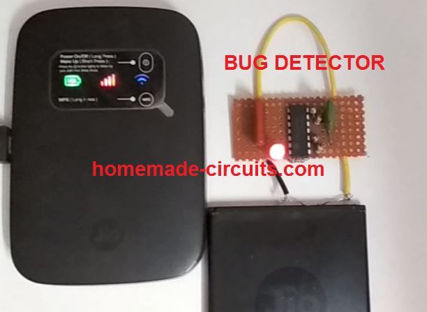
The bug detector circuit presented here is exclusively developed by me, and can be used for detecting, pinpointing any hidden wireless device or unwanted surveillance planted in a room.
The hidden spy devices could be inside beds, cupboards, tables/chairs, flower pots, or in fact anywhere a normal individual would least suspect.
Identifying such hidden unwanted surveillance system can be impossible without using costly and sophisticated equipment. However, the circuit idea presented here is not only cheap to build, it also accomplishes the job with utmost perfection.
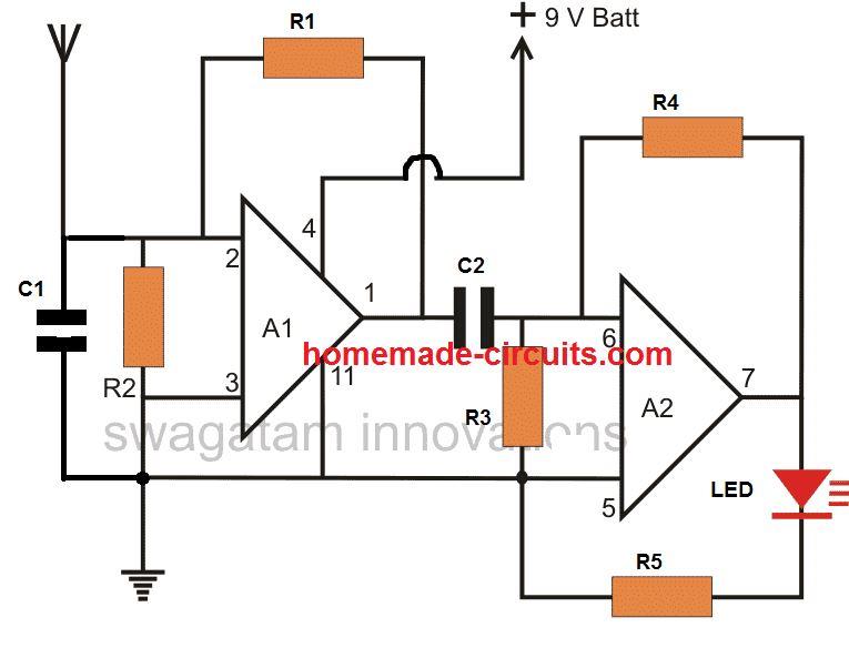
The complete circuit diagram can be seen below:
Video Test Result


NOTE: the sensitivity of the circuit can be adjusted to much higher levels either by increasing the 2M2 resistor value, or by adding two more op amp stages in series with the above design, since we already have two extra op amps in spare inside the IC.
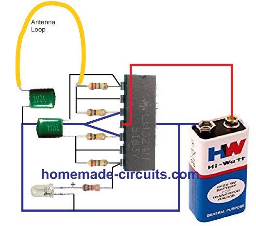
Pictorial Presentation

Circuit Description
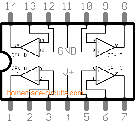
The circuit is basically built using the quad op amp IC LM324. Although the IC has 4 op amps in-built, only two op amps are actually implemented for the bug detector application.
The A1 and A2 stage are identical and both are configured as high gain inverting amplifier circuits.
Since the two amplifiers are joined in series the total gain is highly enhanced making the circuit highly sensitive to RF interference.
Basically the amplifiers work through the following steps:
- The antenna picks up the electrical the disturbances, sends it to the op amp amplifier A1, which amplifies it 10 to 100 times depending on the value of the feedback resistor R1.
- The output from A1 is sent to the next op amp A2 via C2, which blocks the DC ad allows only the picked AC frequency.
- A2 further amplifies the frequency 10 to 100 times depending on the resistor R4. C1 ensures stability to the op amp and avoids stray pick ups.
- R2, R3 ensures the op amp inputs act like differential inputs for detecting minute changes in the received electrical signals.
The circuit is so sensitive that it is easily able to detect all types of electrical noises even thunder lightning interference.
I was surprised when I saw this bug detector circuit easily picking up signals from my wireless Wi-Fi device from a distance of 2 feet. Actually, while the unit was placed on the bed, I found the LED blinking abnormally as if the circuit was unstable and malfunctioning. I was quite disappointed.
Then I picked it up and put it some distance away from the bed, and the LED just shut off. I tried placing it again on the bed and the LED started blinking again. I still couldn't figure out the reason, and thought may be the bed was acting like a large antenna and causing the disturbance.
However, finally I realized that this was happening because my internet WiFi unit was also placed on the same bed at some distance away.
I removed the WiFi device from the bed and the bug detector LED was simply shut off again.
Next, I did a number of repeat tests and was convinced that the unit was actually detecting RF, and the LED blinking wasn't due to an unstable or malfunctioning condition.
Once confirmed I built the final bug detector circuit and presented it here for your reading pleasure!
Parts List
- R1, R4 = 2.2 Meg
- R2, R3 = 100 K,
- R5 = 1 K
- C1, C2 = 0.1 uF PPC
- A1, A2 = 1/2 LM324 op amp
LM324 pinout details can be found below:

Fully Transistorized RF Sniffer, Bug Detector
This small, fully transistorized circuit may be used as a permanently attached transmitter RF monitor, or a close-range transmitter RF detector or both. No tuning coils are necessary! A 9 V transistor radio battery is used to power the gadget.

For transmitter hunting, the loop antenna may only need to be as small as the diameter of a hand (approximately 250 mm) or even less.
You may create a fairly sturdy antenna by engraving a circle or square on a suitable piece of PC board. The other parts might also be mounted on the board.
You might use a folded dipole or a loop that is a wavelength long at one frequency (VHF, otherwise it would be enormous practically).
Transistor Q1 is biased by means of R1 and D1, and changing the bias by means of RV1 allows for sensitivity adjustment.
The antenna loop's signal is corrected by the diode D1-C1. Q1 and Q2 dc-amplify the rectifier's output, forcing a meter deflection in Q2's collector circuit.
At the collector of Q2, any amplitude modulation on the signal received will be displayed.
This is capacitively connected to the base of Q3, amplified, and supplied to dynamic headphones having low or medium impedance and not a high impedance.
This final step may be skipped if simply meter indication is needed.
RF Sniffer Circuit
The circuit diagram for the RF sniffer can be witnessed in the following figure. RF signals heading at ANT1 are connected through C5 towards the detector circuit stage.

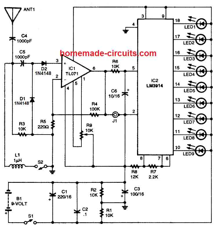
A high impedance ground network intended for wide band detection is supplied by R3.
Having inductor L1 hooked up to the circuit by means of S2, the circuit gets adjusted for the FM band. Diodes D1 and D2 perform the job of detection and demodulation.
The detected RF signal is transferred to the non-inverting input of op amp IC1 .
The IC1 op amp is constructed like a non-inverting amplifier through a preset gain of approximately 450.
The circuit works by using junction field effect transistors (JFETs) at the input sections; which boosts sensitivity because of their high impedance.
Potentiometer R9 works like a squelch control which tunes the IC1 offset settings. The amplified detector output which shows up on pin 6 of IC1 is transferred to J1.
An appropriate high impedance phone could be attached to J1 whenever you would like to hear the detected signal.
Furthermore, R6 and C6 do the job of cleaning the signal. The cleaned up signal is subsequently given to the input of IC2, which is an LM3914 dot /bar display chip.
The LM3914 or LM3915 device includes a network of resistor and a range of comparators.
With respect to the input voltage fed to pin 5, several LEDs will probably light up to show the relative voltage levels.
In this RF sniffer circuit, a 9 LED bar display is set up by attaching pin 3 of the IC2 with the positive supply voltage.
When the detected signal is the weakest, this might illuminate only the LED#9.
As the detected signal voltage becomes stronger, each of the LEDs in the bar graph turns on one by one until, with the most powerful RF signal level, you might find all the nine LEDs being illuminated.
Resistors R7 and R8 are used to fix the reference voltage for a full-scale bar graph LED display.
Observe that we have not used any current-limiting resistors for the LEDs; since the resistors R7 and R8 itself fulfill the function of limiting the LED current.
Parts List

For further inquiries or information please use the comment box below.
RF Sniffer Using IC 741 and Meter Reading
The RF 'Sniffer' device discussed in the following article is capable of detecting RF radiation across a broad range, from approximately 100 kHz to VHF to 450 or 500 MHz, and it will assist in locating and identifying low-power espionage transmitters.
The majority of designers will already have the components in their spares collection (and if not, these are not costly), and the device can be put together in a single evening.
Therefore why not investigate your workplace or house and alleviate those persistent fears?
Circuit Description
The following figure shows the circuit diagram of the device.

A voltage-doubling circuit made of diodes, D1 and D2, and C1 rectifies RE signals captured by a short telescopic antenna. The operational amplifier Cl's non-inverting input receives the resultant dc.
The low value capacitor, C1, and the RF choke, L2, work together as a straightforward high-pass filter to stop the device from reacting to low-frequency ac fields.
In order to bypass low, medium, and some of the higher radio frequencies and further stifle the unit's responsiveness, a lower inductance RF choke, L1, can be switched into the circuit. R1 serves as a load for the voltage doubler, while C2 shunts any remaining RF to ground.
R4 and R5, which control the amount of feedback to the amplifier's inverting input, set the gain of the circuit.
The meter's pointer may be adjusted to zero in the absence of a signal thanks to the resistor arrangement R2 and R3.
The non-inverting input of IC2 is linked to the output of the first operational amplifier. By adjusting the potentiometer R7, which controls the degree of feedback across the second amplifier, the device's sensitivity may be changed.
R9 calibrates the metre to read about 3V FSD and guards against movement damage should the second IC experience saturation. Any erratic variations in the output are smoothed down by C3. S2A and S2B switch the dual 9V-0-9V battery supply into the circuit.
Components
To enhance the frequency responsiveness and sensitivity of the device, point-contact germanium diodes for DI and D2 should be employed (they operate at lesser forward voltages compared to silicon diodes).
A 0.25-watt 1 megohm resistor's body may be made into a suitable small RF choke by winding 30 turns of 34 or 36 SWG enameled copper wire around it. Alternatively, suitable micro RF chokes cn be also procured from an online store.
As an indication, a low-cost signal strength or "VU" meter will work.
These meters typically have a sensitivity of 200 uA, thus shunting or raising the value of R9 will be necessary to provide the necessary 3–4 V full scale deflection. A 1 or 2 mA meter would do for this application with the value of R9 as specified as meter sensitivity is not crucial.
How to Set Up
If D1 and D2 are made of clear glass, they need to be protected from light before setting up the experiment.
When the unit is set to high sensitivity, the photovoltaic impact of the diode junctions is sufficient to swing the metre pointer sharply over.
Inspect the circuit board for poor soldered connections and bridged copper tracks as normal. Also, make sure the diodes, op-amps and C3 are oriented correctly.
Attach the 4K7 preset temporarily in the R3 position (that is, to R2 and pin 5 of IC1, with the slider connected to pin 4 of the IC) and adjust it around mid-way of it rotation.
Turn on the power supply after disconnecting the meter. Each battery should only use about 2.5mA of current.
Replace the 1 mA meter movement with a test ammeter and set it to read 5 or 10 mA FSD. Bring the cursor to zero by adjusting the 4K7 setting.
The default slider is probably going to be significantly off-center. Keep track of whether the potentiometer's higher resistance leg connects to pin 5 of the ic or R2.
The 1 K potentiometer, which will serve as the real set-zero control, should be connected in the R3 position. The preset should be wired in series with the leg that will serve as its high resistance.
Adjust the preset to return the metre pointer to zero after setting the 1 K potentiometer to mid-travel. Attach the 1 mA movement to be used in the Sniffer after disconnecting the test meter.
Making any required tweaks to the preset, confirm that its pointer is capable of being brought to zero with the sensitivity control adjusted to maximum and the I K slider adjusted to zero control at center travel.
Measure the preset resistor's resistance and replace it with a fixed resistor, RX, of the nearest standard value.
When the 4K7 resistor, R2, was connected to pin 1 of the ic, offset nulling was consistently obtained when a variety of 741 op-amps were used in the IC1 position.
Connect the 4K7 pre-set straight to pin 1 of the ic in the unlikely event that the meter refuses to zero (i.e., short out R2).
If you find a null generated with this configuration, pin 5 and R2's connection to the potentiometer must be established.
It takes longer to discuss this setting-up process than it does to actually accomplish it.
Due to the high gain of two cascaded amplifiers, the standard 10K nulling potentiometer that is connected between pins 1 and 5 is impossible to tune.
The nulling or set-zero control has considerably gentler action since just a tiny area of the potentiometer is movable.
The configuration explained above is effective once the setting-up procedure has been completed.
For IC1, a high-quality instrumentation type op-amp having an extremely small input offset current could have been used, however these types of opamps are quite costly (and less likely to be accessible from spares containers).
Switch out L1 and check the RF sniffer by moving it very near to an electromagnetic source.
How to use
It is advisable to test out the device at home before going on a " seek and eliminate" expedition since using the instrument and interpreting the comparison scale readings require a certain amount of expertise and experience.
This is not the place to go into detail on eavesdropping bug circuitry.
It is sufficient to note that basic models of these micro-transmitters operate inside or near the VHF FM broadcast band and emit roughly the same amount of RF energy as a single bipolar transistor, such as a BC547 wired as an LC tuned oscillator and coupled to a short aerial.
This type of circumstance will forcefully knock the indicator pointer over at distances of three to four metres. The sensitivity of this Sniffer circuit is reduced at higher frequencies (450 mHz and above), where more unusual bugs typically function.
However, when the aerial of the device is close enough to the transmitter, it will clearly indicate the electromagnetic field.
The device will detect frequencies down to around 100 kHz when the low inductance RF choke L1 is disabled, and the meter pointer will be repelled by signals emitted by broadcast transmitters that operate on the long and medium wave regions.
Because the house wiring and metal objects (such as bed springs and mirror silvering) amplify these broadcast RF fields, the sensitivity control on the Sniffer must be reduced in order to detect any low frequency transmissions within the structure.
It may be helpful to tweak the set zero potentiometer in order to eliminate constant background radiation.
In order to make the Sniffer immune to bothersome lower frequencies, it should typically be operated with L1 switched ON into circuit.
Micro-transmitters used for eavesdropping typically broadcast at VHF and higher. Despite this, it is most effective to unplug personal computers, VDUs, and TV receivers from the electrical grid while conducting a search.
Certain bug transmitters are intended to be triggered by a phone call to the room or office for a predetermined amount of time.
Before beginning the search, make a call from a nearby room or arrange for the phone to start ringing.
Likewise, bugs may be set up to only broadcast when a phone call comes in, and a link should be established with the "speaking clock" while the survey is being conducted.
Drag the Sniffer aerial over any light fixtures, suspended ceilings, desks, other furniture, artwork, wall clocks, and similar objects.
Consider where you may hide a bug if you were keeping an eye on the space. Brilliant individuals probably have similar thinking.
Let's hope you weren't being overly cautious after all!
How the Circuit Works
C1, D1, and D2 work together to convert the RF voltage that develops across either or both of the input inductors to dc and doubles it.
As soon as the RF voltage changes are negative, a charge is created across C1 that is contributed to the positive voltage swinging.
Operational amplifiers IC1 and 1C2 are both linked in a closed-loop, non-inverting mode with feedback being applied to the inputs that are inverting.
A potential divider across each device's output is the source of the negative feedback.
With this configuration, R4+ R5 / R5 determines the gain of IC1, which is roughly 214.
The gain of this stage may be adjusted between 21 and 304 by introducing potentiometer R7 into the bottom leg of IC2's feedback network. Consequently, the unit's total gain can be anywhere between 4500 and 65000 times.
Op-amps are not infallible, thus there will unavoidably be a little imbalances in the differential input circuitry when there is no signal.
This circuit's maximum capacity for amplifying this modest offset current will cause the output stage to become saturated, hence it is necessary to make arrangements for cancelling it out.
This function is carried out by the ICI's nulling circuitry's potentiometer R3, which is hooked up to it.
Considering the gain offered, it is crucial to alter the offset nulling or set-zero control. In order to lower the control voltage on the potentiometer's track, resistors are arranged in series with it.
By doing so, its activity is constrained to the crucial nulling zone, making it simple to bring the metre pointer to zero.
For IC2, offset nulling is not necessary. By applying the required compensation voltage to IC2's input pin, the nulling features focused on ICI balance the entire circuit.
The metre is calibrated to read about 3V FSD using series resistor R9.
Since the 741's output impedance is so low in this circuit, it can supply enough current to harm a delicate meter movement.
If a meter with an FSD below 1 mA is used, increase R9 or attach a shunt.
In order to avoid abrupt output changes from creating erratic pointer swings, a high-value capacitor C3 is wired across the meter because inexpensive meters are unlikely to have significant electromagnetic dampening.