In this article I have explained how to use the low-cost CD4001 and CD4011 quad 2-input gate CMOS integrated circuits in bistable, astable, and monostable multivibrator applications through forty different manners. We also learn how to enhance and modify these configurations to produce highly improved outputs from these multivibrators.
- When CMOS logic gates are configured with an RC network to generate a continuous ON/OFF switching output, it is called CMOS astable circuit. The output ON/OFF period is determined by the values of the RC network.
- When CMOS gates are configured with external switching signals, generally through push buttons to create alternately latching ON/OFF outputs, it is called CMOS bistable circuit. It is also known as SET/RESET latch circuit.
- When CMOS gates are configured with RC network to produce a single momentary output ON/OFF pulse, in response to an input trigger, it is called CMOS monostable circuit. The momentary switch ON output period is determined by the values of the RC network.
When using 'B' series CMOS, all of the circuits illustrated can function over the full five to fifteen volt supply range.
The CD4001 and C04011 ICs
The layouts and pin connections of the CD4001 and CD4011 integrated circuits are shown in Figures 1 and 2. These two integrated circuits consist of quad 2 input gates. NOR gate operations are delivered by the CD4001, whereas NAND gate functions are handled by the CD4011. The truth tables of each of the CD4001's four NOR gates are demonstrated in Fig. 1.
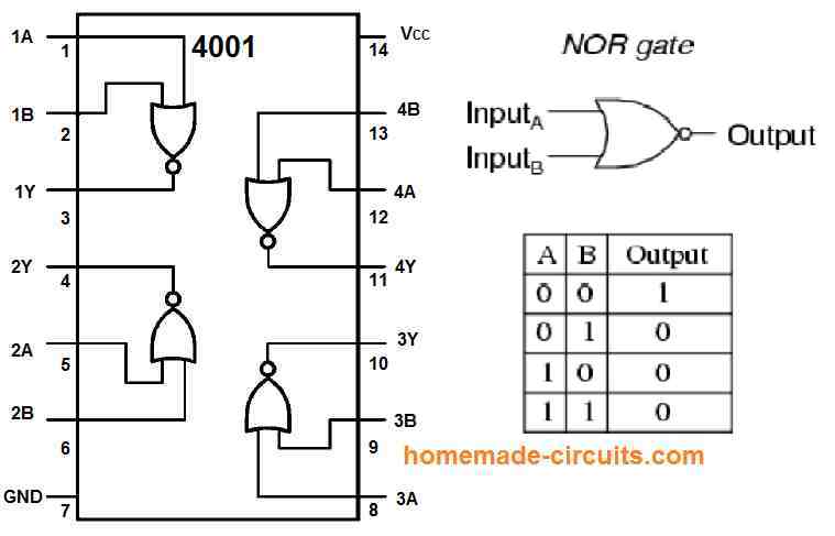
Remember that if both inputs are low, the output is high, but if either one of them or both inputs are high, the output turns low. The truth tables of each of the CD4011's four NAND gates are shown in Fig. 2 below. The output is typically high, and only when both inputs are high does it become low.
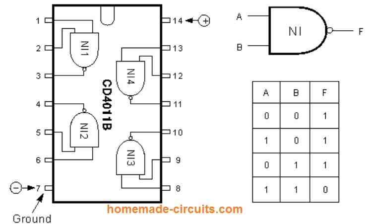
The CD4001 and CD401 1 are low-cost integrated circuits. They are very cost-effective devices that may be implemented in a wide range of practical twin-gate CMOS multivibrator applications.
Bistable Multivibrator Circuits
Both the CD4001 and CD4011 may be utilized in two-gate R-S (Reset-Set) bistable multivibrator circuits, although their input triggering requirements are considerably different. The circuit and waveforms of a pulse-triggered NOR variant of the bistable are indicated in Figure 3. A normal output from ICa and an inverted output from IC1b make up the circuit's outputs.
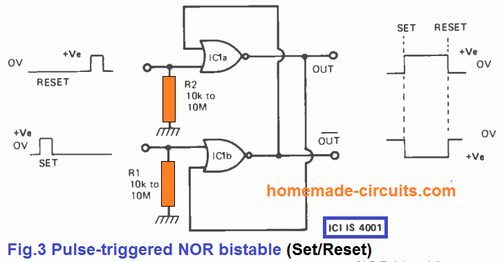
As soon as a positive-edged trigger pulse with a range of about zero to full supply is supplied to the IC1b input, the normal "set" output is turned high and it remains in that condition regardless of any subsequent signals at the 1C1 b input.
In this situation, it is possible to reset the output low only by applying a positive-going pulse to IC1a's input, after which the output turns low and does not get affected to any successive trigger pulses at the IC1a input.
Note that R1 and R2 are used to connect the input terminals of IC1a and IC1b to ground (the zero-volts line): these resistors could have any useful value between 10k and 10M. R1 and R2 can be removed from the circuit if the inputs to IC1a and IC1 b are direct-coupled from previous logic stages.
Manual NOR Gate
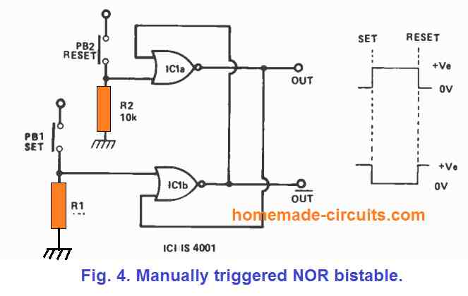
A manually triggered equivalent of the NOR gate circuit in Fig. 3 is shown in Fig. 4. Because the output of this circuit is not affected by the contact bounce, etc. of its two control switches, it is typically called a 'noiseless' switch.
Bistable NAND
The CD4011 NAND gate variant of the bistable circuit is shown in Fig. 5.
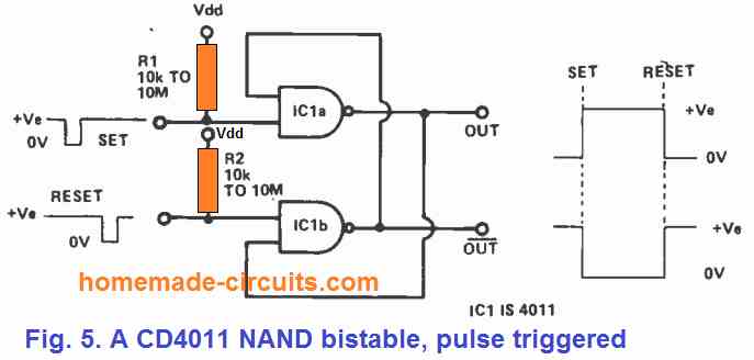
Except for the placement of R1 and R2, this circuit is essentially similar to that in Fig. 3. Note, however, that the NOR gate circuit requires a positive-edged trigger pulses, whereas the NAND gate circuit requires negative-edged pulses, and that the set pulse in the NOR circuit is applied to IC1 b, whereas the set pulse in the NAND circuit is applied to IC1a.
Manually Triggered NAND Bistable.
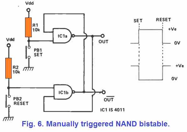
The manually-triggered variant of the NAND-type bistable is shown in Figure 6. Although R1 and R2 are depicted as having values of 10k, they can actually have resistance values ranging from a few thousand ohms to roughly 10M, depending on the specifications of the application.
Touch-triggered NAND bistable
Because of this adaptability, the touch-triggered NAND bistable circuit of Fig. 7 was developed, wherein R1 and R2 have values of 10M and the circuit may be initiated by putting any resistance having a value less than 10M (or example finger resistance) between the touch contacts.
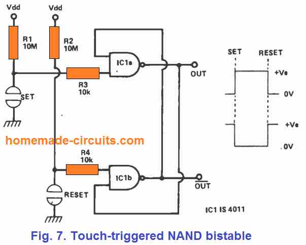
The inputs of the two gates are stabilized by the resistors R3 and R4 in this circuit. All of the bistable circuits we've seen so far employ trigger signals with identical polarity (either both positive or both negative).
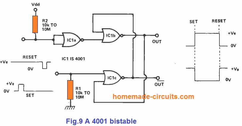
In some applications, however, using reverse-polarity signals to activate the bistable is essential or convenient, and this sort of action may be achieved by connecting an inverter stage to one or both of the conventional bistable input terminals.
Figures 8 and 9 illustrate two different types of this circuit.

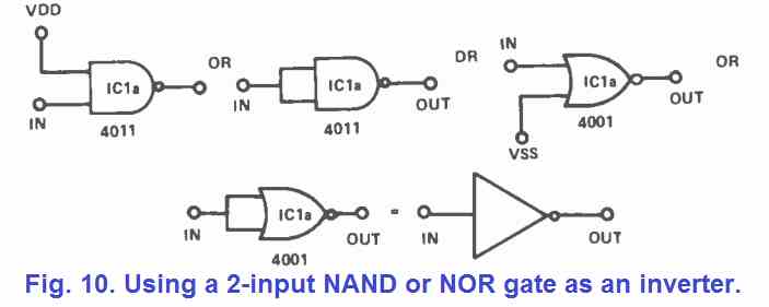
Different methods of connecting a 2-input NAND or NOR gate to serve as a basic pulse inverter stage are shown in Fig. 10. These circuits have a wide range of uses.
Basic 2-Gate Astable Circuits
The CD4001 and CD4011 are both 2-gate astable multivibrator circuits that may be implemented in a number of applications. Because the gates are linked as ordinary inverters in these circuits, both the types of IC provide similar results.
Figure 11 depicts the most simple and practical 2-gate CMOS astable circuit.
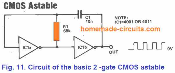
With the comfort parameters provided, this circuit offers a good square wave output, has great thermal stability, and runs at around 1 kHz. Because the frequency is inversely proportional to the C-R time constant, it may be increased by reducing either C1 or R1.
Make sure that C1 a non-polarized capacitor in practice, and its value can range from some tens of picofarads to a few microfarads.
The CD4001 and CD4011 are both 2-gate astable multivibrator circuits that may be implemented in a number of applications. Because the gates are wired as ordinary inverters in these circuits, both the types of IC provide similar results.
R1 might be anything between 4k7 and 10M. In the R1 slot, connect a fixed resistor and a pot/preset in series for variable frequency operation. The output of the Fig. 11 astable circuit swings almost completely between the zero and positive supply voltage limits (using a lighter load). However, the built-in clamping diodes at the input of IC1a prohibit the junction of R1 and C1 from swinging below zero or over the positive rail levels.
As a result of this aspect, the circuit's operational frequency is impacted by supply rail voltages to some extent. As an approximate rule of thumb, for every 1% increase in supply voltage, the frequency drops by roughly 0.08 percent.
When this astable's frequency gets normalized using a 10 volt supply, the frequency reduces by 4% at 15 volts and increases by 8% at 5 volts. Furthermore, the working frequency of the Fig. 11 circuit is affected by the value of the transfer voltage specs of the particular gate utilized, and can alter by up to 10% across different ICs.
The waveform's output symmetry is also determined by the IC's transfer voltage specs, and in most situations, the circuit will produce an asymmetrical output.
The shortcomings of the basic astable circuit tends to be of little practical importance in the large number of 'hobby' and other non-precision applications.
Compensated or Optimized Astable
The 'optimized' astable circuit of Fig.12, in which resistor R2 is connected in series with the input of IC1a, can eliminate some of these shortcomings.

The key objective of the resistor R2, which may be any value between two and ten times that of R1, is to permit the R1-C1 line to swing smoothly between zero and positive supply rail voltages during the switching operation, minimizing the circuit working frequency's reliance on the supply voltage.
When R2 is ten times higher than R1, with the supply voltage varying between 5 and 15 volts, the frequency fluctuates by only approximately 0.5 percent.
Figures 11 and 12 show conventional and the optimized astable circuits that can be constructed with a number of detailed modifications.
Figures 13 through 18 depict a few of these designs. C1 charges and discharges via R1 in the basic astable circuit, as an example.
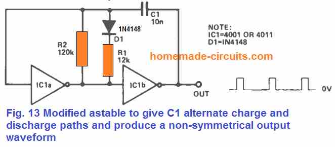
The basic circuit may be changed to provide different C1 charge and discharge channels, as shown in Figures 13 to 15. One method of altering the stable state of the circuit to produce a non-symmetrical output waveform is shown in Fig. 13. C1 charges through one direction via R1 and R2 in tandem, resulting in a high output, however discharges in the other way via R2 individually, resulting in a low output.
On/Off Control
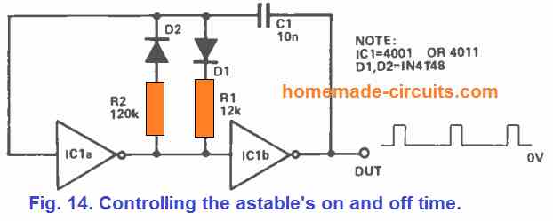
Figure 14 depicts how the circuit may be enhanced by providing a diode in series with R2, allowing R1 to control the ON time of the output while R2 controls the OFF time. By substituting one or both of the timing resistors with a fixed resistor and a potentiometer in series, both these circuits could be modified to produce adjustable outputs.
Variable Duty Cycle (PWM)
Figure 15 explains how to modify the astable to provide an adjustable PWM or mark/space ratio output while the frequency is held close to constant.
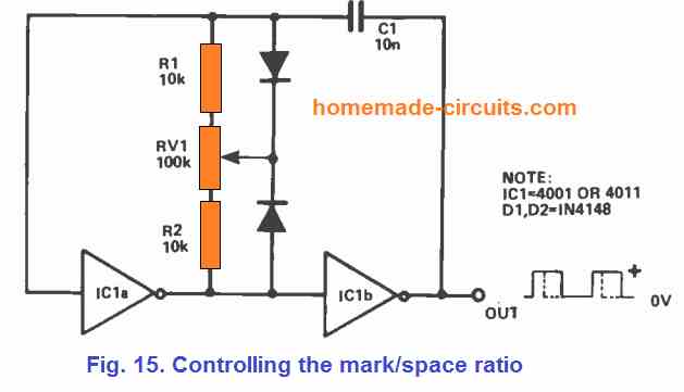
C1 is charged in this circuit through one particular direction via D1-R2 and through 50% of RV1, and in the other direction through D2-R1 and the remaining 50% of RV1. RV1 allows you to change the PWM mark/space ratio between 1:10 and 10:1.
A multi-tone push-button operated astable's circuit can be seen in Fig. 16.
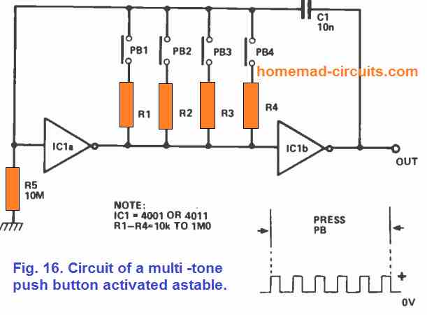
R5 normally keeps the input of IC1a (and consequently the output of IC1b) low while all push-button switches are open. In case any of the push-button switches is closed, the circuit works like a standard astable, because the values of resistors R1 to R4 are all low in comparison to R5.
This circuit may be implemented in multi-tone musical devices, electronic organs, and other applications, and it has the benefit of using very tiny amount of current while in the sleep mode. The number of push-button switches that may be employed with the circuit is unlimited.
Frequency Modulation
Fig. 17 illustrates the method through which the astable could be integrated with a frequency modulation or voltage control of frequency input, simply by connecting an external voltage signal to the input of IC1a through a resistance that is significantly larger than R1.
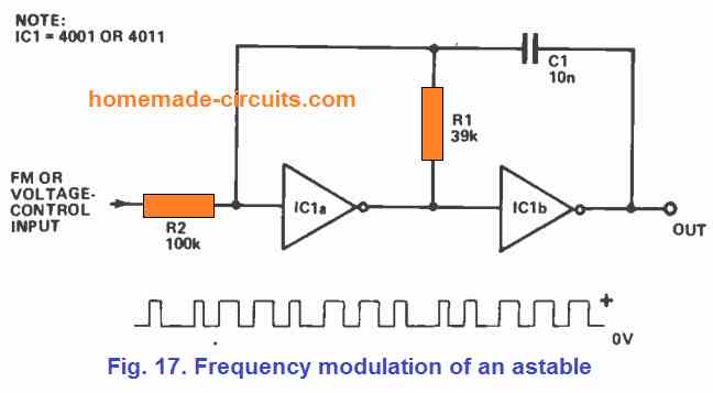
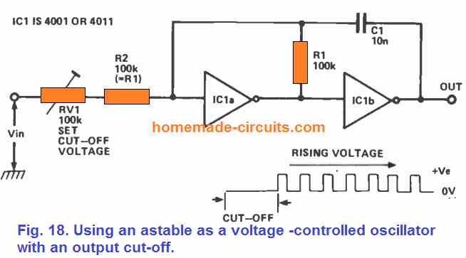
Fig. 18 indicates a simple method through which the circuit could be further enhanced to operate like a specialized voltage-controlled oscillator which is instantly switched OFF as soon as the input voltage drops below.
By simply replacing the IC1a inverter position with a two-input NAND or NOR gate, and assigning the input control signal to one of the gate input pin, each of the astable circuits in Figs. 11 to 15 could be customized for gated operation.
This arrangement allows them to be switched on and off through an external signal.
Gated Astable Circuits
The CD4001 and CD4011 ICs may also be utilized in this application, however their gate control and output functioning can be significantly different. The two fundamental configurations of the gated astable circuit could be seen in Figures 19 and 20.
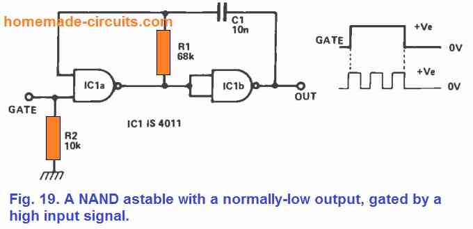
The NAND astable circuit in Fig. 19 consists of a typically low output which is gated through a high input signal, whereas the NOR astable circuit in Fig. 20 has a usually high output which is gated through a low input signal.
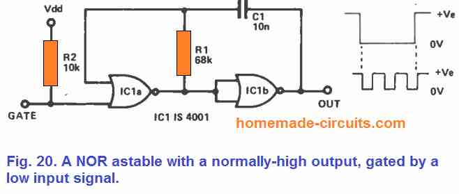
Also, while R2 is depicted in the picture with a value of 10k, R2 may actually have any value between 10k and 10M, or it can be removed entirely in case the signal to the gate is fed via a preceding logic state.
Eliminating Noise Interference
In the circuits shown in Figures 19 and 20, the output signal stops as soon as the input gate signal is disconnected. As a result, any noise interference existing at these circuit gate inputs likewise emerges at their outputs.
Figures 21 and 22 below illustrate how to modify the circuits to correct this flaw.
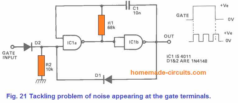
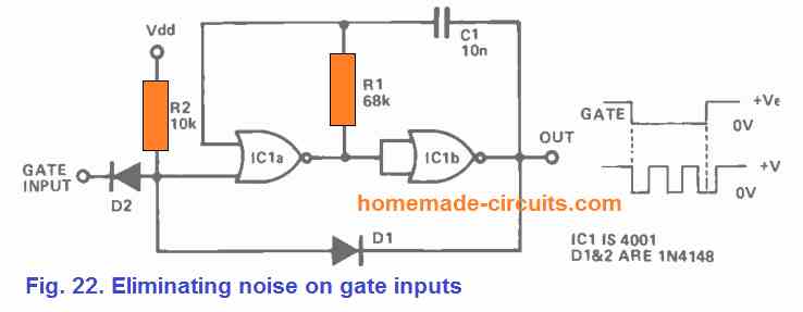
The gate signal of IC1a is obtained through diode OR gate D1-D2-R2 from both externally and the output of IC1b. When the circuit is gated externally by D2, the output of IC1b causes the gating to be stronger via D1 for each half astable cycle, thus removing the impacts of interference in the external signal. The circuits outputs are in the form of full half-cycles.
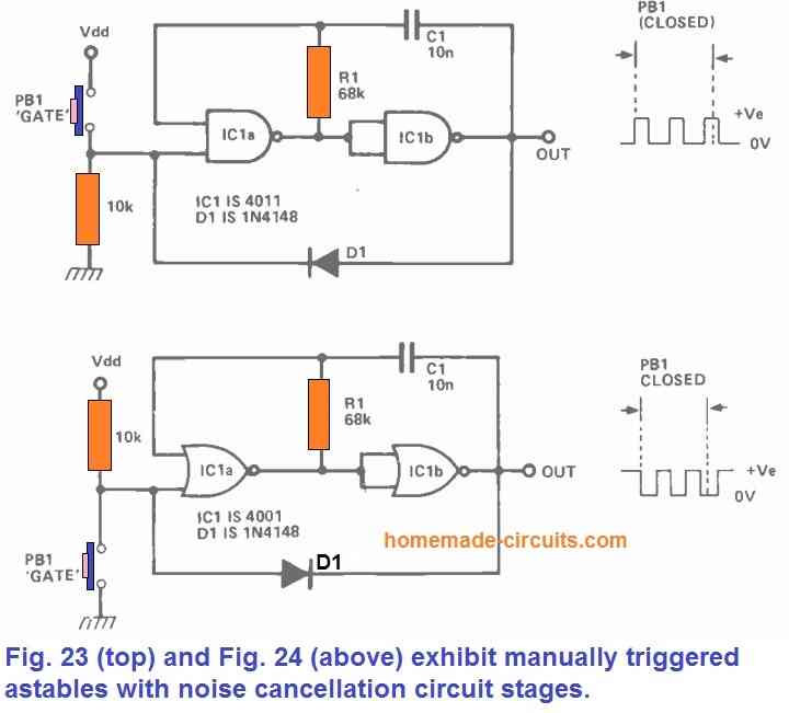
Observe that R2 is an important component in these circuits. The circuits from Figs. 21 and 22 are shown as manual-triggered configurations in Figs. 23 and 24. When push button PB1 is quickly pressed, they create a single crisp clock pulse; while PB1 is pushed down, they create five perfect clock pulses each second. With fast-acting counting and division circuits, the 2-gate astable circuit typically may not be appropriate for direct implementation as a clock generator.
Generating Cleaner Clocks
Precise clock signals having sharp rise and fall times are essential in these circuits. The issue is that 2-gate astables based on "A" series or non-buffered CMOS generate clock outputs having sluggish rise and fall times, whilst 2-gate astables based on buffered-output 'B' series CMOS are designed to generate outputs with excellent rise and fall times, however these may generate "dirty" clocking if their power supply lines happen to have even the slightest level of noise.
Thankfully, all these issues may be readily solved by connecting a few inverter-connected gate stages in series to the astable circuit's output, as illustrated in Figure 25.
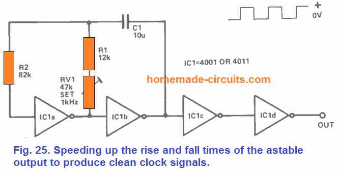
These inverter stages reduce or eliminate the noise impacts on the clock circuit by speeding up the rise and fall periods of the astable output waveform, thus producing excellent level shifting between the astable output and the clock input pin of a given external source.
3-Gate Astable for Improved Output Clocks
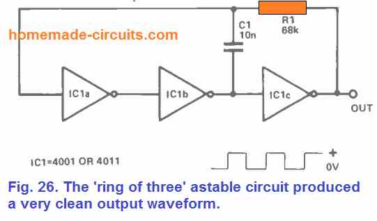
The "3-gate" astable circuit shown in Fig. 26 is another way to implement a clock generator. The locations of R1 and C1 are swapped in this design, and the inverting input stage (1C1a) in the Fig. 11 circuit is essentially substituted by an ultra-high-gain non-inverting stage (consisting of IC1a and IC1b in series) in Fig. 2.
The Fig. 26 '3-gate' circuit offers an excellent clean output waveform with an exceptional rise and fall timings. Therefore, it is highly suited for use as a clock generator due to the extremely high gain of its combined input stages.
The complete fundamental design modifications described for the two-gate astable may be also applied to the '3-gate' astable circuit. For example, in the Fig. 11 circuit, C1 alternately charges and discharges through R1, allowing the circuit to be exposed to all of the modifications indicated in Figs. 13 to 15.
It can be built in the standard or 'compensated' forms, for example. Since it may be gated on and off through either its IC1b or IC1c stages, the '3-gate' astable circuit provides fascinating capabilities when implemented in the gated mode.
Controlling NOR Gates with an External Signal
Figures 27 to 30 depict four different interpretations on the topic. Alternative configurations of the gated NOR-type '3-gate' circuit can be seen in Figures 27 and 28. To turn the astable on, both circuits require a 'low' signal.
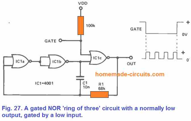
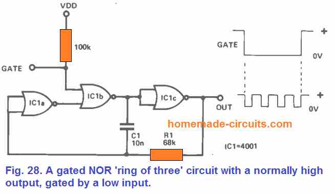
It should be noted that the circuit's output is typically low when IC1c is applied with a gate signal, and typically high when the IC1b is subjected to a gate signal. Identical differences may be observed in the gated '3-gate' NAND design, as indicated in Figs. 29 and 30.
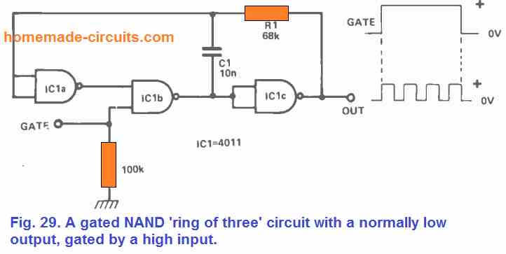
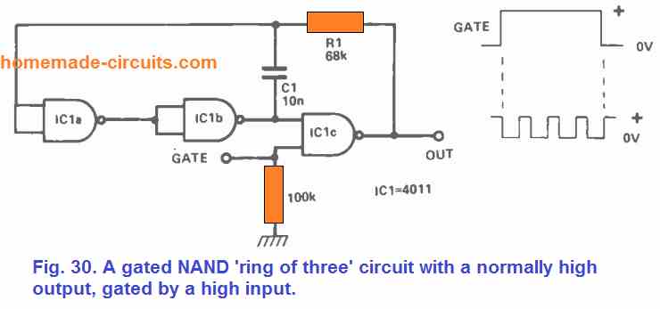
These circuits require a 'high' signal to turn on, and exhibit a typically low output when the gate signal is applied to IC1b or a normally high output with an application of the gate signal to IC1c.
CMOS Monostables
Both the CD4001 and CD4011 may be utilized to build a very useful 2-gate monostable multivibrator or pulse generator circuit.
Figures 31 and 32 illustrate a couple of basic variants of this circuit. The length of the output pulse in these circuits is governed by the R1 and C1 values, which is about one second per microfarad of C1, when R1 is 1M5.
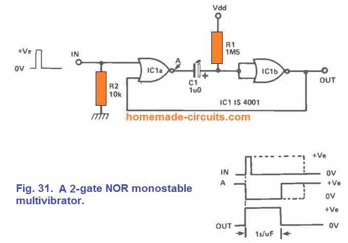
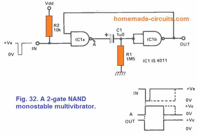
In reality, C1 could use any value between 100p and several thousand uF, while R1 could have any magnitude between 4k7 and 10M. One distinguishing property of these circuits is that the input trigger signal could be directly linked and therefore has no discernible influence on the duration of the circuit's output pulse: The length of the trigger pulse might be shorter or greater than the length of the output pulse.
The NOR type exhibits a typically low output and is activated by a positive-edged input pulse, whereas the NAND type CMOS gate produce a normally high output and is driven by a negative-edged input pulse.
The pulse signal arriving at point "A" has the same duration as either the output pulse or the input trigger pulse, determined by the signal which is the larger of the two. This function is useful for creating pulse-length comparators and over-speed monitors, among other things.
There are just two substantial imperfections in the circuits shown in Figures 31 and 32. One of them is that the pulse length is influenced by the transfer voltage specifications of the particular IC in the circuit.
The second defect is that the pulse duration is affected by the level of the supply voltage employed in the circuit, in the same way as the operating frequency of a simple two-gate CMOS astable is affected by the supply voltage variations.
However, in the majority of implementations, these flaws tend to be insignificant.
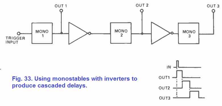
An inverter stage must be inserted between the outputs and inputs of consecutive monostables to execute the right polarity trigger signals in case several of the Fig. 31 and 32 circuits are to be coupled for generating cascaded delays (as in a delayed-pulse generator, for instance).
The fundamental mechanism block diagram can be seen in Figure 33.
Sound Generator Alarm Call Circuits
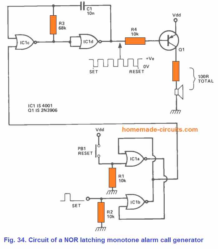
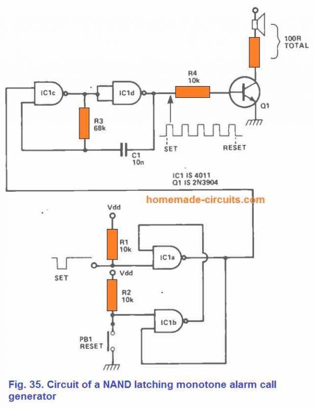
A CD4001 or CD4011 IC with one or more transistors may be implemented to create a range of highly effective sound alarm system designs. Some experimental circuits of this kind are presented in Figs. 34 to 41.
The circuits can be operated in all situations through any source using the 5V to 15V range and may be employed with any 3R to 100R speakers. Depending on the speaker impedance and the supply voltages chosen, the output power may range from many hundreds of milliwatts which could be increased simply to 10 watts by including extra power boosting transistor stages.
Two variants of a monotone latching signal generator are displayed in Figure 34 and 35. IC1a and IC1 b are interconnected and the 1C1c-IC1d-1 kHz astable tones are connected to the IC1a-IC1b bistable automatic latches and switches. By temporarily shutting PB1, the circuit could be reset to the OFF mode.
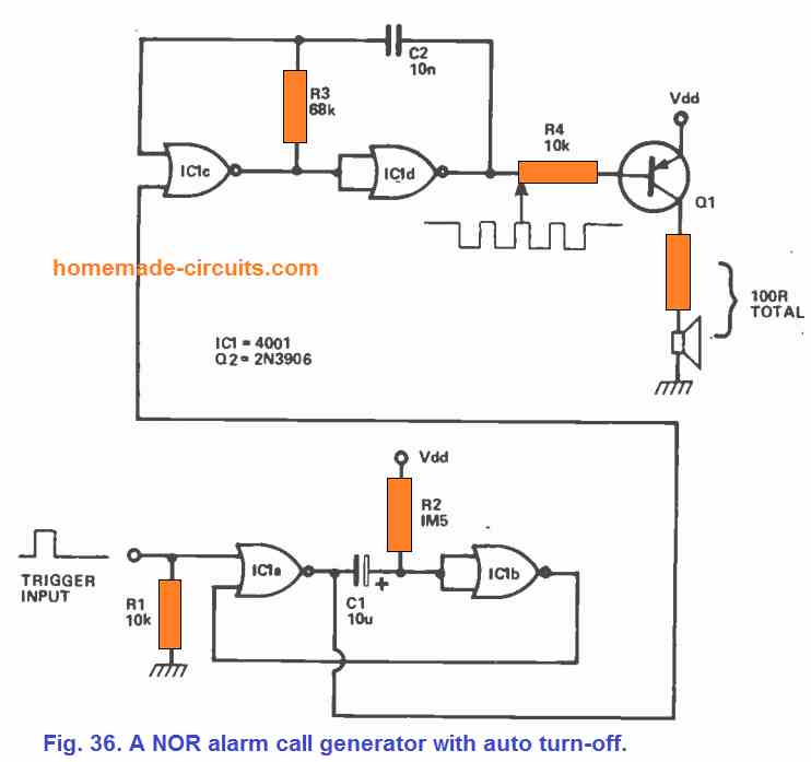
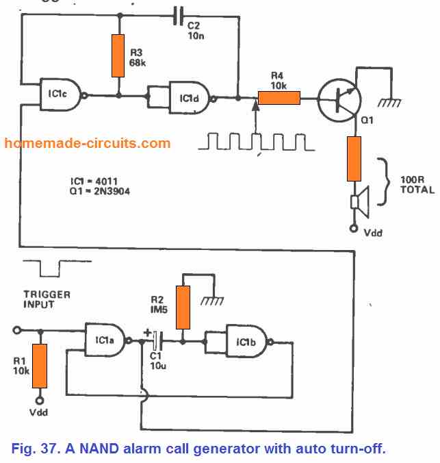
The auto-turn-off monotone alarm generator implementations can be seen in Figs. 36 and 37. IC1a and IC1b can be seen connected as a monostable multivibrator and whenever the IC1c-IC1d are activated, it switches on the astable for approximately 10 seconds.
When a proper control signal is provided to the input of IC1a, the circuits in Figures 38 and 39 create a pulsed-tone signal which allows a 1 kHz astable (IC1c and IC1d) to be gated on and off through a 6 Hz astable (IC1a and IC1b).
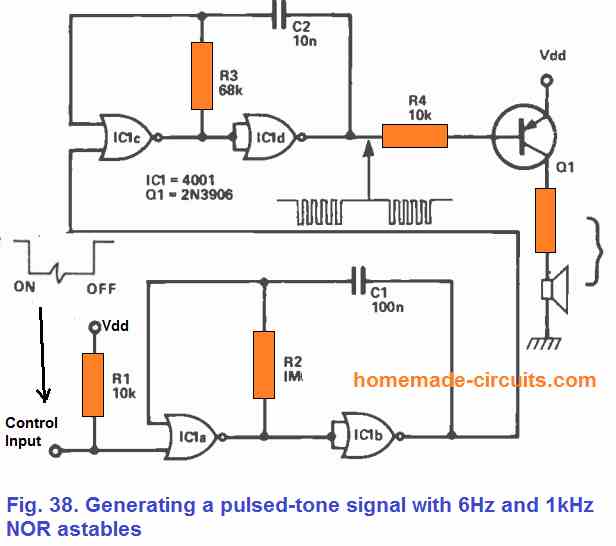
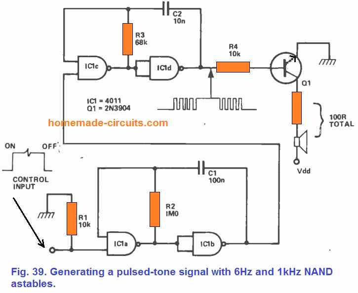
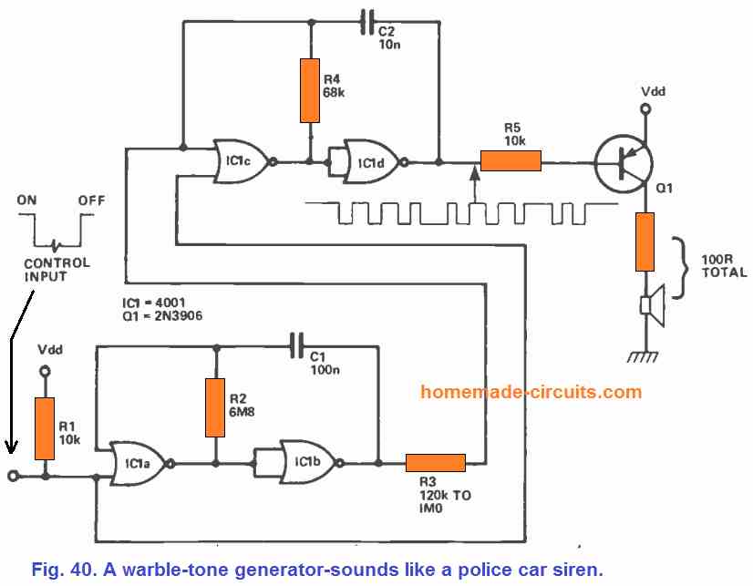
This results in the generation of a pulsed tone signal. Lastly, Fig. 40 illustrates a warble tone generator that creates a sound comparable to a British police car siren by switching across a 2-tone cycle during each second, in response to an appropriate control signal introduced to the inputs of IC1a and IC1c. R3, that can be selected to have any value in the approximate range of 120k to 1M, determines the intensity of the circuit's frequency fluctuation.
I am not sure from the cct. Diagram for connecting two 4017’s if the 4001 uses the input power feeding the 4017’s.
Please advise, I am a novice.
Sorry, I did not understand how you want to configure the 4017 with 4011??
Dear Swagatam,
Thank you very much.
Glad to help, Zoki!
Where are figures 23 and 24?
OK, I have updated them now, please check it out…
Dear Swagatham,
Where are figure 23 and 24?
Thank you Zoki, I think I forgot to insert those images and now they are lost permanently. I had referred the article from an old magazine, and I don’t have that magazine with me now.
Dear Swagatham,
I need your help. I was having a very old 500 watts servo stabilizer bought in 1992. it was lying in the house , having some complaint that I forgot. Today I thought to have a look at it. Found it was not working correctly.
Om examination found it was using 4011 be NAND gate. On one output there was a transistor to-30 package. It was rusted fully and the pin too broke. I want to replace it. I would like to know what type of transistor it could be ? it it driving a relay that switches on and off AC main output line. I have a hunch thatit is NPN and could be something like 2N3019. But would like to have your opinion
rgds
Dear Suresh, for the transistor I think a 2N2222 will be a good choice, since it will be able to handle almost all types of standard relays regardless of the coil resistance.
Dear Swagatam,
Thank you very much for the suggestion.
rgds
You are welcome Suresh!
Hi, I hope this is the right topic for my question. I have a solar charger with a dry contact option where it will close the contact if the battery voltage goes below a threshold and open when it the voltage goes back above another threshold. This is to connect to a generator to start it to charge via 120V and then stop it when charged. My generator has a momentary switch for starting and stopping. So I need the contact close to generate an inching switch and then when it opens generate another inching switch. Can you point me to either an existing module or help with this project? Thank you.
Hi, I did not understand inching switch function, do you mean a flip-flop action for switch? Or maybe two switches which will latch across two different contact points alternately?
Fig 1 is supposed to be the truth table for the 4001 NOR gate. Fig 1 is properly labeled but it is for an OR gate and truth table.
Thank you very much for pointing out the mistake, I have replaced the first diagram with the correct one
hello , I was very happy to see those project posted to me , thanks ,