In this article I will comprehensively discuss 7 accurate RC square wave oscillator circuits with 50% duty cycle, by appropriately configuring the gates from various CMOS ICs such as 4001, 4011, 4093, 4046, 4047, 4016, 4060 etc. and also using op amps.
Definition
The square wave oscillators included in this article can be defined as circuits built using CMOS gates or op amps for generating accurate frequency outputs, having perfect square waveform with 50:50 duty cycle, or symmetrical ON/OFF pulses.
It means, the waveform from these RC oscillator will have a perfectly square in shape with equal ON and OFF time periods. Moreover, being from CMOS ICs, these frequencies are digital in nature, and therefore can be expected to be more reliable and accurate than the BJT based analogue type of square wave oscillator designs.
CMOS Oscillator
CMOS devices give you a wide range of opportunity to design of R-C oscillators. RC oscillators can be built equally using standard gates and with ICs created specifically for oscillator circuits.
Having inputs which work with around 1 / 2 the supply voltage and outputs which could switch right across positive and negative supply voltage, CMOS gates are perfectly suitable for stable oscillator design.
Circuits employing these tend to be less complicated plus more efficient compared to identical models designed with discrete units like transistors.
Their minimal power necessity and wider operating voltage range between 3 to 15 volts additionally make them perfect for use in battery-powered circuits.
You may find a few issues though, which needs to be recognized and these are going to be thoroughly discussed in this article.
1) Using NOT Gates
The fundamental prerequisite for the majority of R-C oscillator circuits can be a set of inverting gates attached in series as displayed in the following Figure 2.1.
Let's assume that the input is to gate G1, both inverted and noninverted outputs are together accessible, through G1 and G2 respectively.

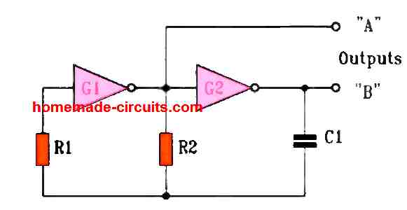
The working of the square wave oscillator using a couple of NOT gates, let's say from the IC 4049 is straightforward to understand.
Circuit Description
Assuming the output from G1 at the instantaneous positive changeover, the resulting positive input to G2 can cause its output to become negative and this negative signal will move via capacitor C1 and resistor R1 and return to the input of G1, speeding up the activity until a total transformation of state for both the gates has transpired.
The positive output from G1 can subsequently begin charging C1, slowly increasing the voltage at G1 input.
As soon as it extends to 1 / 2 the supply voltage G1's output will yet again start to change state, on this occasion to negative, and the entire cycle will keep repeating.
Frequency Formula
The time period necessary for each half-cycle will be 1.1 x R x C, therefore the frequency can be presented as:
f = 1 / 2.2 RC
where R is R2 and C is C1 in the circuit. Appropriate values for R2 resistor can be between 10 k and higher, and for capacitor C1 the value can be between 100 pF and higher.
The voltage polarity across C2 will keep reversing, therefore C2 cannot be a polarized capacitor like an electrolytic, nevertheless any other non-polar will do. For improved stability polystyrene and polyester capacitors are advised.
Two outputs can be found, a single from each gate. Either one or both of them could be utilized. Their working is opposite with their polarity, a characteristic which can be typically helpful in many of the circuit designs.
How to Adjust Frequency
The frequency could be altered through a variable resistor for R2, as well as the duty cycle could be tweaked by means of diodes and resistors.
Yet again, it is the period of time which is governed by this resistor, therefore the frequency output results is going to be non-linear.
Even though it is straightforward and trustworthy, you will find certain possible drawbacks with this circuit that consumers should know about.
First of all, the output duty cycle is hardly ever uniform. To get a proper 50:50 ratio or a extremely small frequency, please refer to the next circuit idea which incorporates a divider IC.
Secondly, for approximately 10 kHz the output frequency usually adheres to the above equation, however beyond this value it starts getting less and less consistent, normally it is less than what the equation gives.
The frequency is additionally dependent on the supply voltage variations, usually the frequency will show an increase as the voltage is increased, and yet again this impact may start getting more visible at higher frequencies.
CMOS Oscillators Require Less Current
CMOS gates are widely recognized for their minimal supply current specifications however this applies specifically when their inputs are being operated mostly near to the supply limits.
While working with intermediate input voltages CMOS output stages can run with partial conduction causing higher current draw.
Also, gradually increasing potential at CMOS gate input may result in instability and "glitches", or spikes, close to the switching points.
The issue can be generally hidden unless of course checked using a fast oscilloscope.
Such glitches can cause the IC to behave unpredictably and cause errors if the signal is employed, for instance, to operate a counter.
This issue could be generally remedied by simply introducing a 10k resistor in series with the load or the the counter in our example.
Together with the counter's input capacitance, this 10k can form a low-pass filter that is normally quite enough to correct the issue.
Schmitt Trigger Oscillator
An alternate strategy could be the utilization of "Schmitt" gates, for example the gates from the IC 4093B quad Schmitt NAND.
However the hysteresis of such ICs can have an affect on the frequency measurements and an increased frequency deviations, along with disparities in supply voltage.
The use of Schmitt gates is not going to stop the higher current consumption issue either.
All these aspects must not dissuade hobbyists from using these square wave oscillators though, since CMOS oscillators are straightforward, inexpensive and dependable and in the majority of applications it works with no issues.
As long as the possible stumbling blocks are recognized, the reason for unforeseen side effects could generally be quickly identified and removed.
How it Works
The function of resistor R1 is crucial. At the time when the G2 output begins chnaging state, let's imagine to positive, the side C1 pin conected with the G1 input is at 1 / 2 the supply voltage.
As G2's output toggles, the G1 input gets higher at first to logic 1 and a 1 / 2 the value of the supply voltage.
Exactly the same thing takes place for negative output which also changes, only in the reverse direction with the G1 input falling to 1 / 2 the supply voltage below negative supply line value.
Many B-series CMOS ICs include internal protection circuitry which safeguard their own inputs from these voltages to avoid static discharge destruction.
This safety feature may be available in different forms according to the supplier, although typically includes diode networks organized to switch ON whenever voltages over or under the input supply are linked to them.
In the R-C oscillator circuit this could cause fast early discharge of C1 when its voltage go beyond the supply input ranges.
This could negatively impact efficiency and stability therefore R1 is introduced to limit the current flow to the protection, significantly minimizing the bad consequence.
This resistor value must be fairly high compared to R2, usually a ratio of 4 to 1 or higher may be enough.
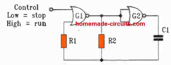
Despite the fact that Figure 2.1a displays a circuit employing a couple of simple inverter gates, it could be designed with NOR or NAND gates as indicated in Figure 2.1b and 2.1c, that make use of gates from a IC 4001B and IC 4011B respectively.
Extra inputs could be linked with each other, or to positive/ground supply line, or these may be used as shown for manipulating the oscillator. In circuits where a four-gate IC is employed the left over gates could be utilized for other preferable or desired requirements.
A pair of square wave oscillator circuits could be constructed using 4 NAND Gates from the IC 4011.
One oscillator can be used for audio frequency generation, while the second one for running at 1 or 2 hertz frequency. Integrating the two with each other would provide a, interesting pulsating audio output as given below.
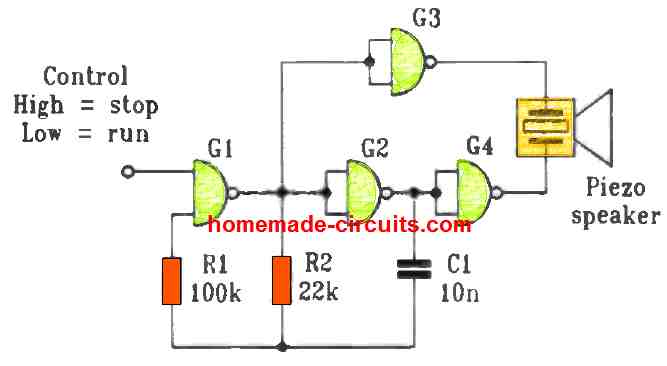
The extra gates could possibly be utilized as buffers to protect against loading of the oscillator circuit.
A practical advice is to try using these for operating a piezo transducer unit, utilizing the 2 gates like buffers with opposite output polarities to make a "bridge" driver circuit.
This design is demonstrated in Fig.2.1c having G3 and G4 configured as buffers.
The majority of of the inverting CMOS gates may be applied for making this kind of RC square wave oscillator circuits. A few ideal varieties can be visualized in the below given listing:
- 4000B Dual 3-input NOR gate plus inverter
- 4001B Quad 2-input NOR gate
- 4002B Dual 4-input NOR gate
- 4011B Quad 2-input NAND gate
- 4012B Dual 4-input NAND gate
- 4023B Triple 3-input NAND gate
- 4025B Triple 3-input NOR gate
- 4093B Quad 2-input Schmitt NAND gate.
It might be feasible to apply the 4070B quad EX-OR and 4077B quad EX-NOR ICs, because these 2-input gates can be utilized as inverter gates if either of the inputs are hooked up to the proper supply voltage line.
Using the 4070B this can be positive, for the 4077B it may be negative. Yet again, this gives an alternative facility to manage the oscillation using these inputs.
2) CMOS 4060B 14-stage Ripple Counter with Internal Oscillator
An effective variant of the simple RC oscillator could be obtained from the CMOS IC 4060B oscillator ,and divider IC.
This is basically a 14-stage binary counter-divider, but as opposed to the some other ripple counters, a set of inverter gates can be seen readily configured as an oscillator, and internally attached with pins 9, 10 and 11 of the IC.
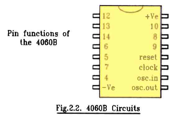
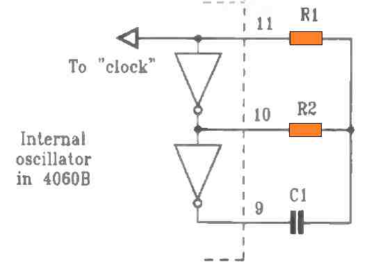
This setup could be applied in a variety of applications, the standard being as a RC oscillator as demonstrated in Figure 2.2c below.
All of the earlier features pertaining to this sort of twin gate RC square wave oscillator is applicable to this 4060 design too, such as the operating frequency that can be determined using the formula:
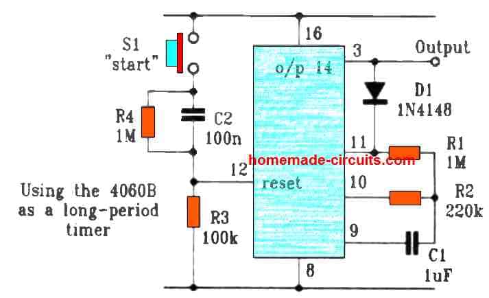
f = 1/(2.2 x R2 x C1).
R1 executes exactly the same functionality as earlier and you can find comparable restrictions around the maximum reliable frequency.
The input for the 2 gates, which is pin 11, is likewise internally attached to the "clock" input of the divider, offering a number of handy possibilities. The output could be extracted from one of the divider outputs.
- The outputs of the IC 4060 are multiple figures of one full RC oscillator cycle, and all outputs feature the exact 50:50 ratio duty cycles.
- The outputs are all buffered, therefore it is not possible to cause loading with these outputs. These could even be utilized for directly driving low-current LEDs, which can be at times great for building cost effective counters or timer circuits.
- The divide/by approach causes this IC to be particularly appropriate for the development of extremely low frequency oscillators using standard value resistors and capacitors.
- Unfortunately, the 1st three outputs are generally not accessible to the consumer. The first externally obtainable is the output 4, at pin 7, that works with 1/16th of the clock frequency. Yet another drawback is the missing output 11, which represents the clock divided by 2048.
- This missing output sequence can be frequently cause a hassle because the IC could normally be excellent for creating very basic binary "addresses".
- The "Reset" input, to pin 12, must be attached to negative supply line for normal functioning. In case it is connected to the the positive supply each of the outputs goes low and continue to be in this state as long as the reset is not switched to the low state.
- The RC oscillator configurable outputs at pins 9 and 10 can also be driven at the low state as long as the reset pin12 is held high with a positive link. Thus, the pin12 could be used for controlling the oscillator functioning of the IC.
- Just like any other CMOS inputs, the reset pin12 must never be kept unconnected as it may give rise to unusual and unstable consequences.
3) CMOS 4016B Electronic Switch Gate Oscillator
One more CMOS device which you can use to construct a twin-gate RC square wave oscillator is the 4016B quad "analogue switch".
This chip consists of four electronic "switches", all of which can be "closed" through the implementation of a positive control voltage.
When a couple of of these switches are configured like inverters, they work like just every other inverting gates forming a CMOS RC oscillator stage. Figure 2.3a below exhibits the connections of the pins for this IC.
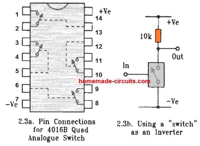
Be aware that, just like various other CMOS ICs, unconnected or extra inputs of the IC must be always terminated to either positive or negative supply, line and should never be left "hanging".
Figure 2.3b above demonstrates the way a solitary switch could be organized like an inverter. One end of the switch is linked to ground line whilst the other is attached to the positive supply line via a 10 k resistor.
Although the control input, marked as "in" in the schematic, is attached to a negative voltage line, the connection of the switch and resistor, marked as "out", becomes "high" in response to a positive voltage through the resistor.
As soon as the input pin is subjected to a positive source, the switch activates and drags the junction between the switch and resistor "low", to the negative supply level.
Considering that the resistor value is sufficiently less compared to the load which the "gate" is going to be operating, the set up offers an efficiency just like any other type of inverting gate.
In case it is used like an oscillator, a couple of these "inverting gates" are built through four pairs of switches from IC1, and all the standard oscillator ingredients are included in the circuit, as displayed in Figure 2.4a below.
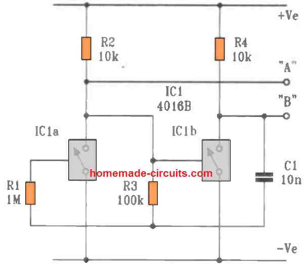
A couple of outputs are offered, indicated with "A" and "B".
Frequency from these outputs, when scanned with an oscilloscope, look quite "untidy", with snags and instability across the switching regions, as well as the frequency which could be accomplished with this circuit is pretty small, although completely sufficient for acoustic applications.
Current Drain Issues
A minor problem with the circuit is that one or other gates is usually in the "on" state, therefore you will see a non-stop current drain by means of the connected load resistor.
Just like the other CMOS RC oscillators, the frequency of this circuit could be determined using the formula f = 1/(2.2 x R x C).
The actual results can deviate from the value of the formula, more consistently as we go on increasing the frequency rate.
This means that the formula should be used just like a guideline prior to practical experimentation while designing such CMOS based square wave oscillators, and the real frequency should be confirmed only through an oscilloscope or a frequency meter.
Stability Issues
The circuits's frequency is actually pretty stable to variations in source voltage and ambient temperature. The duty-cycle is also fairly close to a 50:50 ratio.
Just like with many of the other 2 gate CMOS oscillator circuits, it is possible to change its output frequency by upgrading R3 through a diode and resistor networks.
However the response of this circuit is sluggish, and calls for a couple of additional resistors leading to a little higher current consumption.
Therefore why must anybody take the trouble of building an oscillator using switches available from this IC 4016?
The reason is just like the majority of the other CMOS oscillators I have explained in this article, this specific oscillator circuit works with a solitary low-cost IC, however here the "unused gates" are a actually a couple of extra analogue switches, featuring a pair of opposite-phase outputs readily available, which could be implemented through various innovative techniques, such as as a two-way switch etc.
When CMOS gates from these electronic switches are used for making a square wave oscillator, they efficiently eliminate the spikes and transients or other glitches normally present around the logic switching thresholds, to provide much cleaner results, and moreover along with digital signals these switches can also be configured to control the DC voltages and analogue signals well.
CMOS Analogue Signal Control
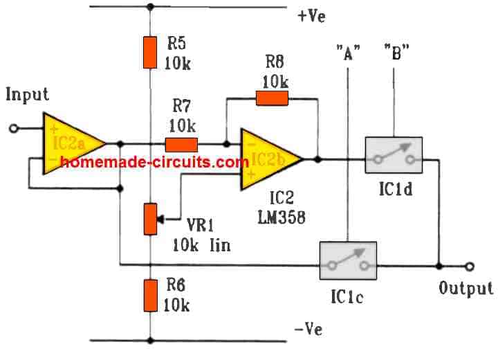
The circuit displayed in Figure 2.4b utilizes a double op-amp, having an amplifier IC2a applied as an input buffer to enable the control signal from a low impedance source, and the second amplifier IC2b, is configured to operate like a unity-gain inverter that produces a complementary signal to IC2a.
Both these voltage outputs are subsequently hooked up to a "2-way switch" created using the rest of the two 4016B electronic switches IC1c and IC1d, to ensure that an varying audio signal amplitude but constant average DC value can be obtained from its output.
Main Features
- The majority of dual op-amps must be well suited for this simple circuit, however the one tried in this article incorporated the common and cheap LM358.
- Despite of being simple this circuit offers outstanding efficiency and has unlimited application range depending on the user's imagination.
- For the beginners, you can try this circuit in the form of an output stage that detects "null" or zero crossing in a DC bridge circuit.
- The pot VR1 indicated in the circuit enables you to offset any sort of quiescent voltage to ensure that any difference in the DC input, positive or negative, can be instantly audible.
- Because our ear carries a logarithmic sensitivity to sound, an extremely big dynamic range can be covered, together with great sensitivity at lower levels.
4) CMOS 4047B Square Wave Oscillator
This IC 4047 is actually slightly distinct from the previously discussed CMOS ICs due to the fact that its basic objective is to work like a flexible timer and oscillator.
Therefore, this IC is effective at working most efficiently at increased frequencies.
Although oscillators in many cases are created using a couple of free gates from CMOS ICs configured for implementing other primary functions, if the designer intends to make a very basic square wave oscillator or requires enhanced functionality this IC 4047 can prove to be extremely handy.
Different pin connections enable the IC to be applied in a variety of different ways, like an astable oscillator with two output modes, complementary outputs and reset, or like an monostable timer with positive or negative triggering.
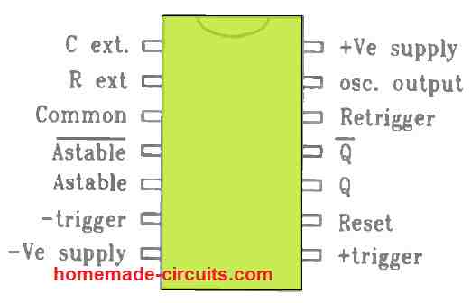
The pin characteristics for the 4047B can be understood through Figure 2.5 above, configured using the standard attributes of a CMOS RC oscillator.
The circuit can be seen working with just one capacitor and a single resistor, and is all that is required to set the frequency.
This frequency value, as earlier can be found out using the formula f = 1/(2.2 x R x C).
Where R may have just about any value from 10k to as high as 1M, while capacitor C ought to be higher than 100pF and should not be a polarized capacitor.
Getting 3 Oscillator Outputs
When an oscillator circuit is configured using the IC 4047, you get 3 oscillating outputs from the IC. The first one is the "Osc out" at pin13, which is a buffered output and working with the fundamental oscillator frequency.
This may not be confirmed to give you an ideal 50:50 duty cycle, however practically it is usually a lot superior to the earlier explained two-gate type CMOS oscillator circuit set ups, particularly at lower frequencies.
The other a couple of outputs that we get from the IC 4047 are "Q" and "Q_", from pins 10 and 11 respectively.
We get these outputs from an internal single-stage divider circuit ensuring that they have accurate 50:50 duty cycles. However they operate at 50 % rate of the principal oscillator frequency which is available at pin13.
These outputs are buffered internally, and work complementary to each other. Meaning, when one of the two pins is positive the other is negative and vice versa.
Main Applications
This IC 4047 can be used for various different applications, you can use is as a piezo sounder device connected across the complementary pin 10 pin 11 so that the piezo is driven from a bridged output with increased volume.
This kind of piezo driver functions wonderfully, generating a significantly loud sound even from your 5-volt supply.
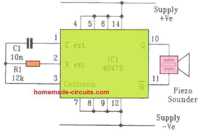
The configuration for this design can be witnessed in Figure 2.5 above, which provides an output frequency of around 1.9 kHz, an appropriate frequency for the majority of piezo sounders. This square wave oscillator frequency can be calculated using the formula:
f = 1 / 2.2 x R x C
However it must be recalled that only the output from pin 13 of IC 4047 runs with the above rate. The outputs from pins 10 and 11 operate at one half this frequency, therefore this could be determined using the formula:
f = 1 / 4.4 x R x C
Main Features
The working efficiency of the IC 4047 is normally a lot improved compared to either basic two-gate circuits or the internal oscillator such as the 4060B.
With excessive frequencies the output frequency value resembles a lot more tightly to the formula results.
A test circuit using 100pF and 22k, designed to get a calculated output of 206kHz, in fact generated 173kHz using a 10 V supply voltage, that appeared much closer than the oscillator using 4060B that could reach only as near as 100kHz using the identical scenarios.
Deviations for the input supply voltage is much less also, at 5 volts the 4047 oscillator circuit continued to maintain to operate at 155 kHz.
In case a realistically stable RC oscillator running at around 100 kHz is intended, then this 4047 IC is possibly the best option.
5) Using 4046B Voltage-Controlled Square Wave Oscillator
A totally different kind of square wave oscillator circuit might be discovered inside the 4046B "phase-locked loop" IC. This extremely versatile chip offers an important feature, for creating very simply voltage-controlled oscillators.
Regrettably explanations for this are often hard to understand for the newcomers, specifically because it provides a couple of independent external frequency control wiring. But in reality it is fairly simple to operate, which we can learn from the following sections.
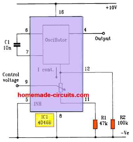
The fundamental wiring diagram for the CMOS 4046 oscillator can be visualized in Figure 2.6, that features a tremendously simplified model of its internal framework.
How it Works
The frequency is defined through an external capacitor C1 hooked up across pins 6 and 7 which is current controlled, the value for which can be fixed externally through the wiring across pins 9, 11 and 12.
The timing capacitor could have any value from 50pF and higher, however this should not be an electrolytic type or a polarized type since the attached circuitry inside the IC is designed to operate by alternately reversing the polarity while charging and discharging the capacitor.
Using the indicated component values in the diagram, the circuit will generate an output frequency of approximately 2 to 61 kHz.
You can find a couple of distinct routes by which the circuit designer may be able to fix the oscillator control current, and it may not be important to work with both of them.
Typically the primary one is set by means of pin 11. Control current runs through the oscillator to this pin via an in-built voltage controlled resistor, which has a value adjusted by an external control voltage put on pin 9.
Pin 11 is generally linked to the ground line through a resistor, which is indicated as R1 in the schematic. The control voltage may extend from zero to the full supply voltage.
When the control voltage is zero, the internal resistor attains an infinity value which means no current can pass through pin 11, and when the pin 12 is not connected, that will stop the oscillator.
As the control voltage is increased the internal resistor gets more and more conductive, hence more current passes through it causing the oscillator frequency to increase.
As soon as the control voltage extends to the positive supply limit, the pin 11 current is restricted primarily by resistor R1, and therefore this resistor is generally known as the maximum frequency setting resistor.
Current may also be allowed to pass via a resistor from pin 12 to ground, indicated as R2. This current can be constant, irrespective of the control voltage, and this resistor is usually known as the minimum frequency setting resistor.
Having said that, since this resistor is used to produce a constant frequency increase, right across the control range, it may be preferable to visualize this like a positive frequency "offset" resistor.
For example, if the circuit had been setup to work through the range between 0 to 20 kHz with R1 and C1, then incorporating a resistor between pin 12 to get a lowest 51 kHz may modify the range to 5 to 25kHz.
Once we understand the current-controlled nature of this IC 4046 CMOS square wave oscillator, through a couple of independent controlled current pathways, it might be much convenient to use this IC.
This offers a very easy solution to control frequency using a voltage input, and the range covered might effortlessly end up being 1000:1 or higher, or this could be decreased to some very small fraction using an appropriate value of R2.
The voltage control input of the IC offers a extremely large impedance, therefore it may be applied with high impedance signal inputs with no need for any buffer stages. The output offers a fantastic 50:50 duty cycle, plus the optimum frequency could be set up quickly from lower frequencies to as high as 2 or 3MHz.
The output frequency is fairly linear with the control voltage, even though there exists little bit of shifting at around less than 20% of the supply. Additionally, it allows you to stop and start the frequency, simply with the aid of pin 5, which works like the "inhibit" input pin.
Although this pin must generally be wired with the negative supply rail, connecting this pin with the positive line will cause the oscillator to halt.
Drawbacks
Sadly there exists a drawback with this particular IC, as it has a few major difficulties associated with stability and varying characteristics across devices.
These disadvantages causes the IC to be excluded from many applications for which it could initially look perfect.
Undoubtedly the main concern seems to be the lack of stability in response to changes in supply voltage.
As an example, a demo circuit put together to operate at 10 kHz using a supply of 15 V slipped down to 6.8 kHz at 10 V and dropped further to 2.1 kHz at 5 volts.
This means that while using practically, this IC might always require a regulated supply voltage where its efficiency may be the lowest at 5 volts.
One possible thing could be to regulate an available 5 V supply and then employ a voltage doubler circuit to raise to a stable 10 V level for the CMOS oscillator, however this hassle would mean the circuit would no longer be simple as in its original form.
A randomly collected 6nos of 4046B's were experimented with within the same circuit configuration, which produced frequencies through 9.9 kHz to 12.7 kHz, indicating that numerous applications would require "select-on-test" manipulation for the right functioning.
You may also find the IC 4046 having a minor sensitivity to variations in temperature. The large deviation of frequency due to changes in the voltage level makes it hard to present a formula for selecting R and C accurately.
Calculating Frequency
However using a supply input of 10 volts a reasonably accurate result could be achieved through the formula:
f = 2 / C x R
The above formula is applicable to the two pins 11 and 12, when it comes to pin 11 the formula takes into account the full positive supply voltage at pin 9.
When the supply voltage is half, the frequency may be approximately half the formula value. The resistors connected across pins 11 and 12 to the ground or the negative line must not exceed the values between 10 k to 1 M.
Even though it is normal to run this IC using a resistor across pin 11 as being the key frequency-setting element, it is rather feasible to keep this pin unconnected and unused, and employ just a single resistor across pin 12 to establish a constant square wave frequency.
As a result, it may be possible to employ a significantly larger resistor between pin 11 to ground in order to present a smaller voltage controlled range of adjustment.
This feature isn't usually apparent in explanations on this IC, however it may be worth trying this, since it can uncover several helpful applications for this CMOS IC 4046.
High Power Square Wave Oscillator
This high-power audio oscillator generates a powerful audible frequency through a piezoelectric transducer.
All 4 gates available from the 4093 lC are utilized in this assignment to operate the transducer through an excellent audio signal. The circuit may be used in wireless house alarms, toys and games, as a separate project to instruct regarding square wave oscillators.
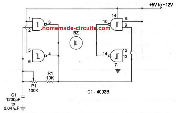
The proposed piezoelectric transducer produces highest output power between 700 and 3,000 Hz, however it may likewise run in different square wave frequencies with less power.
Power supply voltage range can be between 5 and 12 volts. Current usage is determined the power supply voltage, varying from 10 to 50 mA typically.
P1 changes the tone frequency. C1 could be re-structured with a a lot of different values as suggested in the schematic diagram.
6) Square wave Oscillator using Op Amp
Figure below exhibits the circuit diagram of a basic square wave oscillator using a single operational amplifier.
The indicated values provide an running frequency of roughly 1kHz, however this could be modified by altering the R1 or C1 value.
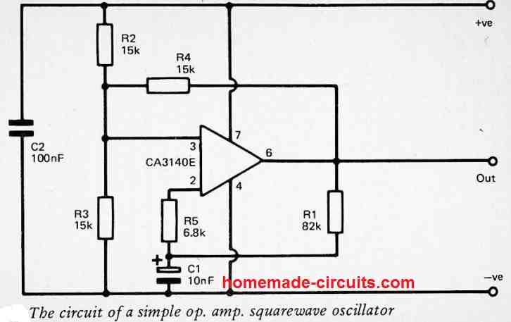
Tweaking these values would provide an inversely proportionate variation in the output frequency. The equation shown below facilitates determining the rough value for the output frequency:
Frequency = 0.82/R1C1
R1 could be any value between couple of kilohms to many Megohms, and C1 can be selected to have a value between a few tens of pF and higher.
The diagram indicates the appropriate polarity for C1 in case a polarized type for example an electrolytic or a tantalum capacitor is employed here.
The highest operating frequency can be 100 kHz or higher, however with extremely high frequencies the output waveform may show some degradation because of the restrictions added to the circuit through the slew rate of the IC CA3140E.
An operational amplifier has no high current output stage, and with no extra output amplification you possibly can obtain an optimum output current of just a few milliamps.
Similar to 555 astables, this circuit is pretty stable in terms of output frequency, and supply voltage fluctuations will not generate major frequency alterations.
The circuit can work nicely using a supply DC as low as 6 volts, and the overall high supply Dc up to 36 volts (which is the highest the CA3140E operational amplifier can tolerate).
The circuit can work with other operational amplifiers, for example LF351, TL081CP, etc., however remember that several of these offer a reduced peak to peak output voltage compared to CA3140E (which allows an output voltage swing of almost equal to the supply DC with a low output load conditions).
A downside of this can be a minor upsurge in the output frequency which may be normally close to 10%.
This op amp square wave oscillator circuit is advantageous in applications where an adjustable frequency square wave oscillator is necessary since the working frequency could be adjusted using a solitary resistance, which is basically needs to substitute the resistor R1 with a fixed resistor and a potentiometer attached in series.
Obviously, the 555 astable circuits explained in one of the earlier posts may also be used like an adjustable frequency oscillators when one of the timing resistances is swapped out with a fixed resistor and a pot connected in series.
However, this arrangement might result in an alteration in the output waveform as the pot is turned for varying the output frequency. This situation may possibly be unfavorable in a few applications.
7) Square Wave Pulse Generator Circuit
The above op amp square wave circuit can be easily customized to generate a pulsed output waveform. The following figure illustrates the required alterations.
This actually includes just a a couple of timing resistors (R1 and R2) along with two driver diodes D1 and D2. The configuration ensures that C1 charges through R2 and discharges by means of R1.
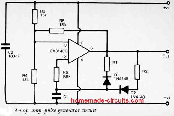
Therefore R1 fixes the low switch OFF output period and R2 determines the high switch ON output period, along with the mark-space duty cycle ratio equivalent to the ratio of R1 to R2.
The working frequency of this square wave PWM pulse generator could be determined through the formula as given below:
Frequency = 0.82/[(R1 + R2)/2]C1
Adjustable Frequency and Adjustable Duty Cycle Square Wave Oscillator
With this op-amp squarewave oscillator configuration, you have the flexibility to achieve a wide range of mark-to-space ratios.
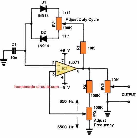
This is made possible by the arrangement where diodes D1 and D2 separate the feedback paths for charging and discharging C1.
RV1 is responsible for adjusting the in-circuit resistance during both charge and discharge phases, thus allowing you to modify the mark-to-space ratio.
You can adjust it within a range spanning from 1:11 to 11:1. Furthermore, potentiometer RV2 enables you to vary the frequency across a 10:1 range, ranging from approximately 650 Hz to 6.5 kHz. RV3 serves as an output level control.
Square Wave Oscillator with Adjustable Mark Space Ratio
Using this straightforward modification, it is possible to change the mark:space ratio of a basic CMOS ring-of-two oscillator across a very large range.
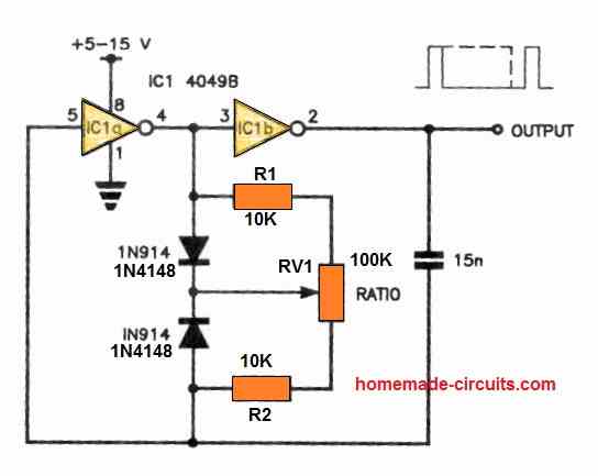
In the configuration depicted, a pot and two diodes have been added to the timing resistor.
The upper diode charges the capacitor via the lower portion of the pot, the lower 10k resistor, and pin 2 of IC1 b, which is low, while pin 4 is high.
This is accomplished by shorting out the top 10k resistor and the upper section of the pot.
The upper portion of the pot, the bottom diode, the upper 10k resistor, and pin 4 are all used to discharge the capacitor when pin 4 is low.
The charge and discharge times, and subsequently the mark:space ratio, are determined by the wiper's selection of the pot's percentage.
Here, one might get a change from 1: 1 1 to 1 1: 1. Increase the capacitor value for a lower frequency. Reduce the capacitor value to increase the frequency.
Hi Swagatam. Thanks for sharing the above circuits, the accompanying info was also very useful. I have 2 questions. 1) I built the 4093B circuit above which I figured to be a driver for a passive buzzer but I had active buzzers on hand so I tried both. The resulting output running on 3.7 li-po battery was a slight pulsing of the diaphragm using passive buzzers and a low beeping for the active buzzers. It works quite well when I put the buzzer in a transistor switch circuit and use your output to trigger the base of the transistor. I get the nice loud beeping I was looking for. Not sure why I couldn’t get that using the circuit as you had it. Tried 3v and 5v active and passive. Thoughts? 2. More importantly since it does work with the transistor. How could I apply your mark, space diagram above to the 4093B circuit to get a beep…stop…beep…stop tone. Thanks.
Thank you Richard,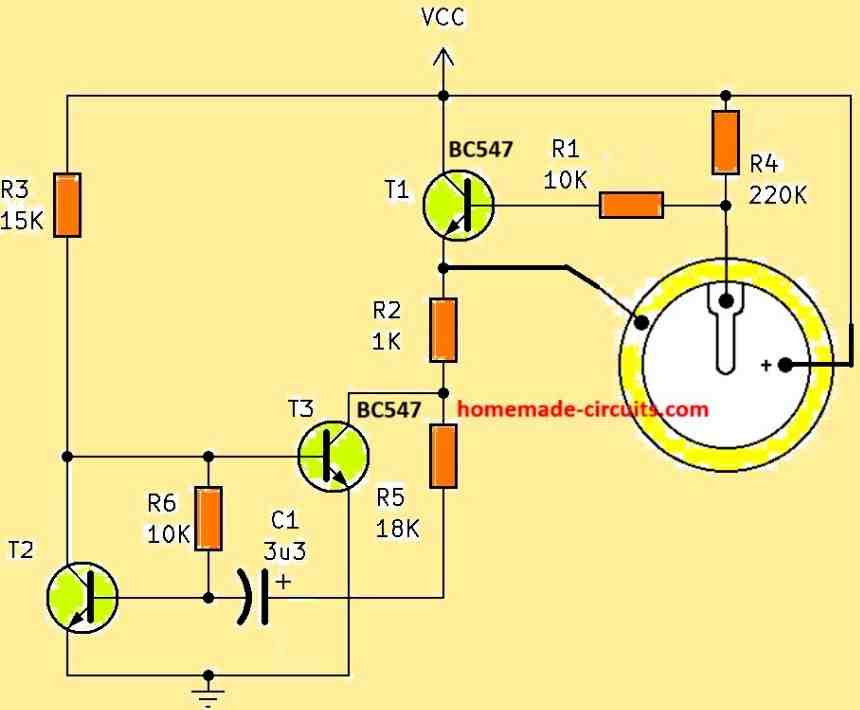
Actually the above circuits are not designed or tested by me, these were acquired from external sources. I think the transistor might be helping to induce higher amount of current and voltage, enabling the higher output.
For intermittent output you can probably try the second last circuit from the following article:
https://www.homemade-circuits.com/simplest-piezo-driver-circuit-explained/
You can use your 4093 IC nand gates for this circuit.
Alternatively you can also try the following transistorized design:
" rel="ugc">
Let me know how it goes.
Thanks Swagatam, appreciated. Will let you know how it goes.
Hello, sir
I am interested in your discussion about the square wave oscillator using IC CD4011, as we know that the IC CD4011 output is on pins 10 and 11
can you help me make an inverter circuit using cd4011 ic with an output of 300 watts or more
Hello Augus, You can try the following concept. The diagram indicates a 4093 IC but you can replace the agtes with the IC 4011 gates. The transistors can be replaced with mosfet IRF3205
" rel="ugc">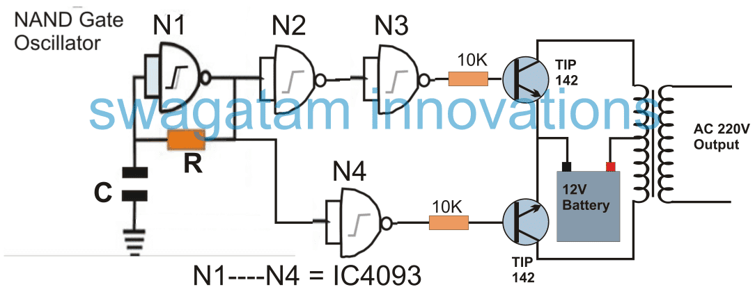
Can I copy and paste someone else’s web address sir, because my question is related to this,Sir
You can do it, I will delete the link afterwards.
Good morning Sir,
So I have been out of this end for long enough to not remember tips, tricks, AND basics! I need a 5 VDC controlled fixed 5Hz signal at 50% duty cycle fixed w low power consumption. preferably mA’s but I think I can go as high as 1 amp. I am not sure the power supply would function at the 1A limit. So let’s cap the current draw at 500mA’s. Your assistance on this would be greatly appreciated!
Respectfully,
Frank Stanek
Hi Frank, you can use one of the designs presented above, and connect a transistor at the output for supplying the required pulses at 500 mA current. You can also use a transistorized version as explained in the following article:
How to Make Any Light a Strobe Light Using Just Two Transistors
Additionally an IC 555 version can be also tried for getting a 200mA output directly from the IC:
IC 555 Astable Multivibrator Circuits
Good morning Sir,
Yes; I like the IC 555. I was looking at using a 220K for R1, a 20K for R2, and a .68uF for C1 to get my 5Hz at 50%. 5VDC as VCC.
Sure, you can go ahead and use the IC 555 square wave astable design as explained in the linked article.