This configuration is known as common-emitter configuration because here the emitter is used as the common negative terminal for the input base signal and the output load. In other words, the emitter terminal becomes the reference terminal to both the input and output stages (meaning common to both the base and collector terminals).
Common emitter amplifier is the the most commonly used transistor configuration can be seen in Fig. 3.13 below for both pnp and npn transistors.

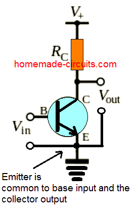
Basically, here the transistor base terminal is used as the input, the collector is configured as the output, and the emitter is wired common to both (for example, if the transistor is NPN the emitter may be joined to the ground line reference), hence it gets its name as the common emitter. For an FET, the analogous circuit is termed as the common-source amplifier.
Common Emitter Characteristics
Just like common base configuration here also two ranges of characteristics again become essential to fully explain the nature of the common-emitter setup: one for the input or base-emitter circuit and the next for the output or collector-emitter circuit.
These two sets are shown in Fig. 3.14 below:
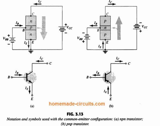
The current flow directions for the emitter, collector and base are indicated as per the standard conventional rule.
Although, the configuration has changed, the relationship for the current flow which was established in our previous common base configuration still applies here without any modifications.
This may be represented as: IE = IC + IB and IC =IE.
For our present common-emitter configuration, the indicated output characteristics are a graphical representation of the output current (IC) versus output voltage (VCE) for a selected set of values of input current (IB).
The input characteristics can be seen as a plotting of input current (IB) against the input voltage (VBE) for a given set of output voltage values (VCE)
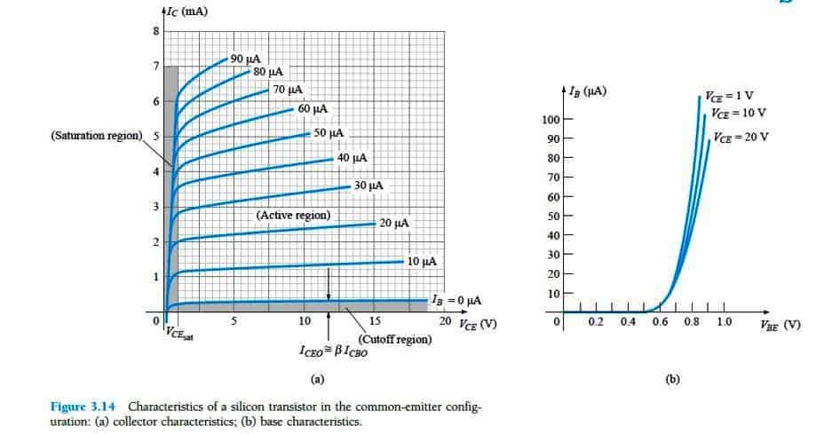
Observe that the characteristics of Fig. 3.14 indicates the value of IB in microamperes, instead of milliamperes for IC.
Also we find that the curves of IB are not perfectly horizontal like the ones achieved for IE in the common-base configuration, which implies that the collector-to-emitter voltage has the ability to affect the value of the base current.
The active region for the common-emitter configuration can be understood as that section of the upper-right quadrant which owns the largest amount of linearity, meaning, that specific area where the curves for IB tend to be practically straight and evenly spread out.
In Fig. 3.14a this region could be witnessed on the right side of the vertical dashed line at VCEsat and over the curve of IB equal to zero. The region on the left of VCEsat is known as the saturation region.
Within the active region of a common-emitter amplifier the collector-base junction will be reverse-biased, while the base-emitter junction will be forward-biased.
If you remember these were exactly the same factors which persisted in the active region of the common-base setup. The active region of the common-emitter configuration could be implemented for voltage, current, or power amplification.
The cutoff region for the common-emitter configuration doesn't appear to be nicely characterized compared to that of the common-base configuration. Notice that in the collector characteristics of Fig. 3.14 the IC is not really corresponding to zero while IB is zero.
For the common-base configuration, whenever the input current IE happens to be near zero, the collector current becomes equal only to the reverse saturation current ICO, in order that the curve IE= 0 and the voltage axis were one, for all practical applications.
The cause for this variation in collector characteristics could be evaluated with the appropriate modifications of Eqs. (3.3) and (3.6). as given below:

Assessing the above discussed scenario, where IB = 0 A, and by replacing a typical value like 0.996 for α, we are able to achieve a resultant collector current as expressed below:
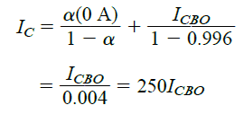
If we consider ICBO as 1 μA, the resulting collector current with IB = 0 A would be 250(1 μA) = 0.25 mA, as reproduced in the characteristics of Fig. 3.14.
In all our future discussions, the collector current established by the condition IB = 0 μA will have the notation as determined by the following Eq. (3.9).

The conditions based on the above newly establish current could be visualized in the following Fig 3.15 using its reference directions as outlined above.
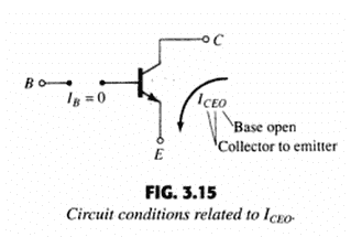
For enabling amplification with minimum distortions in the common emitter mode, the cut off is established by the collector current IC = ICEO.
It means the area just under IB = 0 μA should be avoided for ensuring a clean and an undistorted output from the amplifier.
How Common Emitter Circuits Work
In case you want the configuration to work like a logic switch, for example with a microprocessor, the configuration will present a couple of points of operation of interest: first as the cut off point, and the other one as the saturation region.
The cutoff may be ideally set at IC = 0 mA for the specified VCE voltage.
Since the ICEO is normally quite small for all silicon BJTs, the cut off could be implemented for switching actions when IB = 0 μA or IC = ICEO
If you remember in out common base configuration, the set of input characteristics were approximately established through a straight line equivalent that lead to the result VBE = 0.7 V, for all levels of IE which was greater than 0 mA
We can apply the same method for a common-emitter configuration as well, which will produce the approximate equivalent as depicted in the Fig. 3.16.
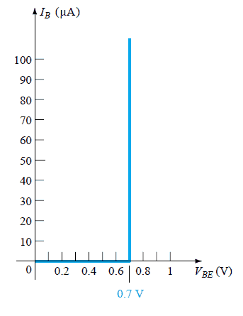
The result complies with or our previous deduction according to which the base emitter voltage for a BJT within the active region or the ON state will be 0.7V, and this will be fixed regardless of the base current.
Solved Practical Example 3.2

How to Bias a Common-Emitter Amplifier
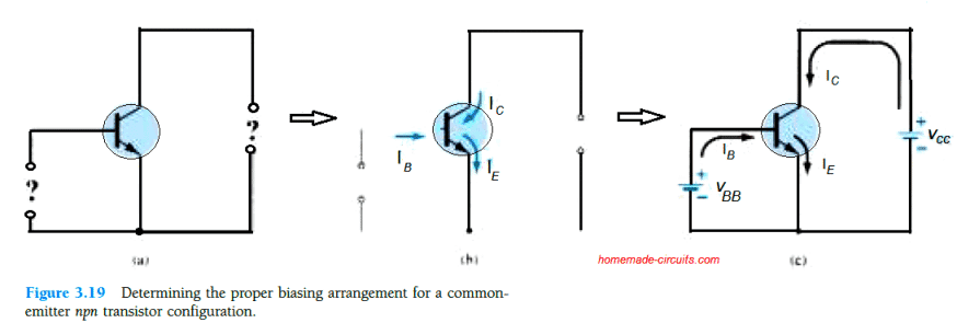
Biasing a common-emitter amplifier appropriately could be established in the same way as it was implemented for the common-base network.
Suppose you had a npn transistor just as indicated in Fig. 3.19a, and wanted to enforce a correct biasing through it, in order to establish the BJT in the active region.
For this you would require to first indicate the IE direction as proven by the arrow marks in the symbol of the transistor (see Fig. 3.19b). After this, you'd require establishing the other current directions strictly as per Kirchhoff’s current law relationship: IC + IB = IE.
Subsequently, you have to introduce the supply lines with correct polarities complementing the directions of IB and IC as indicated in Fig. 3.19c, and finally conclude the procedure.
In the similar manner a pnp BJT could be also biased in its common emitter mode, for this you simply have to reverse all the polarities of the Fig. 3.19
Typical Application:
Low-frequency voltage amplifier
A standard illustration of the usage of a common-emitter amplifier circuit is demonstrated below.
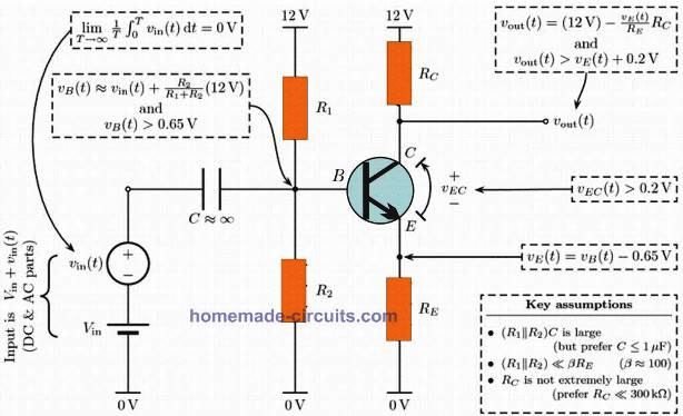
The AC-coupled circuit functions like a level-shifter amplifier. In this situation, , the base–emitter voltage drop is supposed to be around 0.7 volts.
The input capacitor C gets rid of any DC element of the input, while the resistors R1 and R2 are used for biasing the transistor to enable it to be in active condition for the whole range of the input. The output is an upside down replication of the AC component of the input which has been boosted by the ratio RC/RE and moved through a measure decided by all 4 resistors.
Due to the fact RC is normally quite massive, the output impedance on this circuit could be really substantial. To minimize this concern, RC is maintained as small as it can be plus the amplifier is accompanied by a voltage buffer such as an emitter follower.
Radio Frequency Circuits
Common-emitter amplifiers are sometimes also used in radio frequency circuits, such as to amplify weak signals gotten through an antenna. In cases like this it is commonly substituted by the load resistor which includes a tuned circuit.
This can be accomplished to restrict the bandwidth to some thin band structured throughout the desired operating frequency.
More to the point additionally, it permits the circuit to work at bigger frequencies because the tuned circuit enables it to resonate any inter-electrode and run-a-way capacitances, that generally prohibit the frequency response. Common emitters may also be widely used as low-noise amplifiers.

Have Questions? Please Leave a Comment. I have answered over 50,000. Kindly ensure the comments are related to the above topic.
I’ve never been to any electronics school, but I like electronics, please explain the above tutorial in layman’s terms or language. Also you can add, how to come up with resistors to bias a transistor. I would like to know this. I’m tired of finding a circuit and start making a project. I would like to be design my circuits.please help me.
You can refer to the following article, it gives an example regarding how to select the base resistor of a BJT with respect to the collector load:
Transistor Relay Driver Circuit with Formula and Calculations
However practically you will find that the values are never so critical. For example for a 400 ohm relay the formula gives a resistor value of 56K, but practically a 10K resistor becomes sufficient and the transistor works very normally along with the relay.
This seems like the other page here I saw.