

In this post I am going to explain various communication protocols that are used by microcontrollers, microprocessors and ICs for communicating with various sensors, electronic drivers, input and output devices.
We will see:
- Why do communication protocols exist in electronics?
- UART protocol.
- I2C or IIC or “I squared C” protocol.
- SPI or Serial Peripheral Interface protocol.
- CAN – Controller Area Network protocol.
Why do communication protocols exist in electronics?
In electronics various communication protocols are developed and standardized so that sensors, drivers and various input and output devices can communicate with each other seamlessly.
If there were no standardized communication protocols, different manufactures may fabricate sensors, drivers, peripherals etc. in their own way and hardly any sensors and peripherals will be compatible with other manufacturer's specifications and developing a product and debugging / fixing them in such a scenario will be a tedious task.
Each mentioned protocol in electronics is established for specific purposes and circumstances and a product developer may choose one or more according to their needs and specifications.
In this post we will be exploring about four mainstream communication protocols that will be encountered by all embedded system developers and programmers.
Universal Asynchronous Receiver-Transmitter (UART):
UART is a serial communication protocol that transmits and receives data one bit at time from least significant bit to most significant bit.
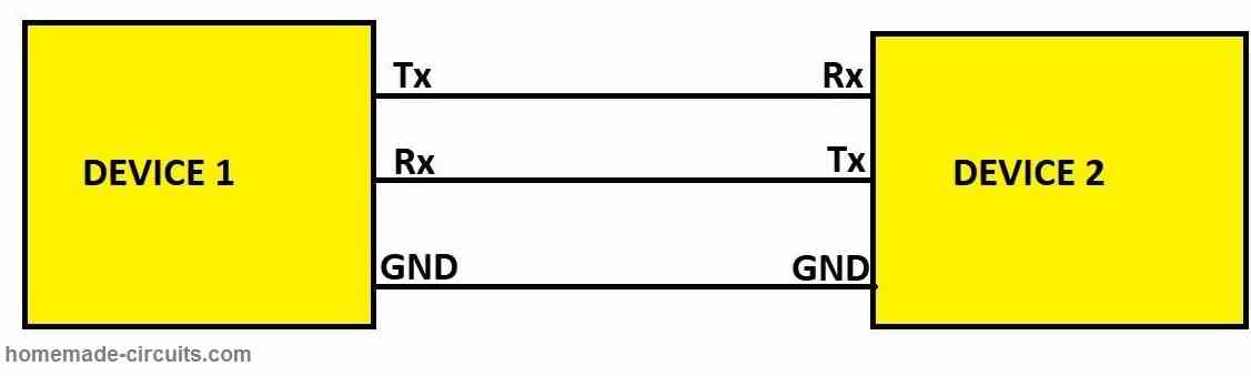
We need two devices for establishing a UART communication and it is full duplex, meaning the data can be transmitted and received simultaneously.
UART communication requires two wires (bus); Tx – transmit, Rx- receive and a common ground for completing the circuit between the two devices. The Tx of one device will be connected to the Rx of the other device and similarly the Rx of one device is connected to the Tx of another device.

The speed at which the data is transmitted or received is called baud rate which is essentially bits per second. The common baud rates are 9600, 115200 etc.
Voltage levels:
The UART data is transmitted and received at two different voltage levels and there are two standards called RS-232 and RS-485. RS-232 operates at 12V and RS-485 operates at 5V.
Data framing for UART:
Data frame or timing diagram is an important aspect of any communication protocol because it describes how the data bits are transmitted, received and synchronized on a communication bus.
A firmware program developer writes a program code based on the timing diagram for proper communication between sensors, microcontrollers and peripherals.

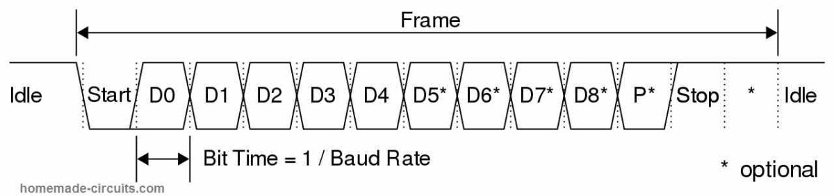
- During the idle state the Tx and Rx lines are pull high and we can see in the above timing diagram.
- When data transmission starts, it always begin with a “start bit”, here the start-bit is transmitted by pulling the transmit line to LOW for some time and after this the actual data bits gets transmitted.
- D0 to D8 are the data bits and this data length can vary depending on the requirement. The minimum length is 5 bits (D0 to D4) and can extend up to 9 bits (till D8). From D0 to D8 the bits can be high or low depending on what you are sending and that’s why the diagram is shown with high and low lines simultaneously. In most applications LSB or least significant bits are transmitted first.
- An optional parity bit can be transmitted and this optional bit is to check the data integrity on the receiving end.
- The next bit is called “stop bit” and this stop bit can be one or two bits in length.
- After the stop bit, the transmit line is pulled HIGH until the next data frame is transmitted.
The time length of a bit is determined by the baud rate and it is time critical. Before transmitting some data from one device to another it is mandatory to set the baud rate of both the devices the same.
Errors in UART communication:
Any communication between two points / devices is prone to errors / noise and UART is no exception. Here is the list of errors that may occur in a UART data transmission and UART is capable of detecting such errors.
- Framing error:
UART will generate framing errors when it does not detect a stop bit at the expected stop bit position in the data frame.
- Parity error:
Parity error is generated when the number of “1” bits in the data frame does not agree with the parity bit that has been specified. Parity error is generated only if the parity check is enabled in the code.
- Break condition:
Break condition occurs when the receiver receives LOW signal for a longer period of time, typically for more than a character time. When a break condition occurs we will also get frame error as no stop signal is received.
Some equipment deliberately sends “break” when baud rates gets mismatched and may initiate a meaningful step to match the baud rate again like resetting the device.
- Overrun error:
Overrun error is generated when another byte of data arrives before the previous data on the buffer memory is read by the processor.
- Underrun error:
Underrun error is generated in UART when the transmit buffer is empty or completed transmitting a byte. In UART this is NOT treated as an error. This error is taken seriously in USART communication.
This concludes the UART protocol.
I2C communication protocol:
I2C is also known as inter-integrated circuit, it is often called “I squared C” in short. I2C protocol was developed by Philips Semiconductors in 1982. I2C communication bus is primarily used for communication between ICs, sensors and peripherals etc. over a short distance within a circuit board.
It is a two wire communication which sends and receives data serially; the two bus lines are SDA – serial data and SCL – serial clock.
The communication mode is half duplex, meaning bi-directional communication but only one device can send data and other must receive and the receiver cannot send data to the other simultaneously.
In I2C the data is synchronized using a clock bus which makes sure the data is sent and received properly.
I2C utilizes open collector / open drain configuration meaning the I2C bus can be only pulled LOW but cannot pull HIGH, so we need to connect two external pull-up resistors on SDA and SCL lines ranging from 4.7K to 10K depending on the specifications.

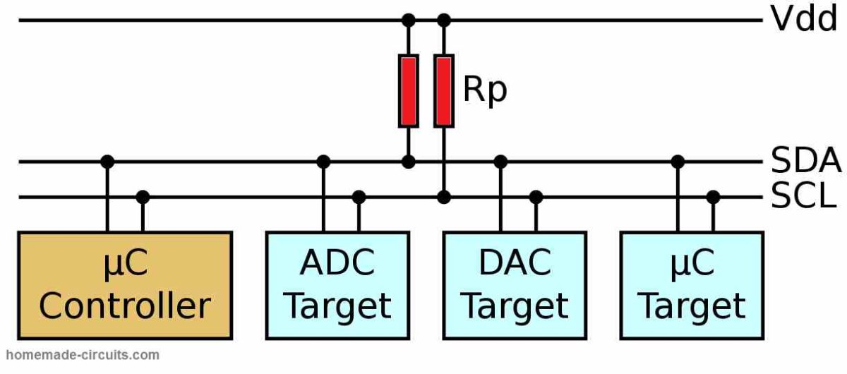
The I2C bus can have multiple master devices and multiple slave devices in the same two wire bus.
The maximum limit of the number of devices that can be connected to the bus depends on the address modes (length).
If the I2C uses 7-bit address for recognizing a master or slave device, then maximum 128 devices can be connected, if it uses 10-bit address, then 1024 devices can be connected on a same bus.
Speed of I2C bus:
- Standard mode: 100 Kb/s.
- Full speed mode: 400 Kb/s.
- Fast mode: 1 Mb/s.
- High speed mode: 3.2 Mb/s.
Note: All data in bits.
Data framing of I2C & timing diagram:

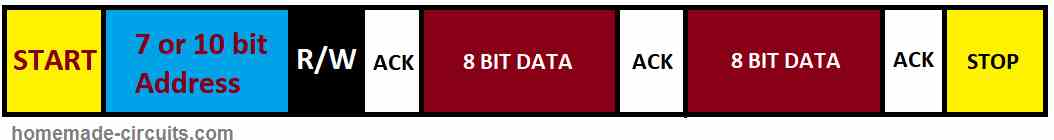

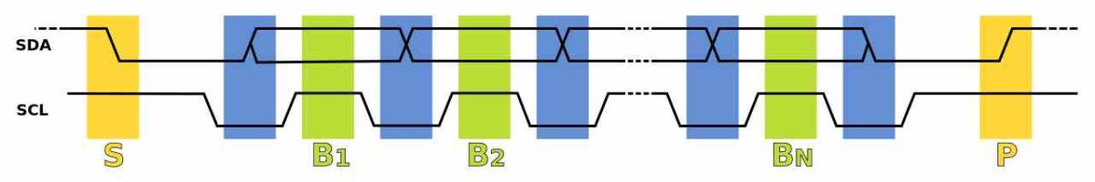
- The communication begins with a start condition; the start condition is satisfied when SCL is at HIGH and SDA changes from HIGH to LOW, you can see in the timing diagram highlighted in yellow ( on left hand side).
- The next piece of data is device address. Every I2C device has an address (7 or 10 bits) so that we can write or read data from that particular I2C device.
- The device addresses are transferred as individual bits just like any other protocols, a bit is allowed to change from HIGH to LOW or LOW to HIGH only when the SCL is at LOW (highlighted in blue). A bit is read by the receiver when SCL is at HIGH – highlighted in green, this is the same for all data chunks. Please note that in I2C the data bits are transmitted from MSB to LSB.
- The next bit is called read / write, the master decides whether the data need to be written or read from the slave device: 1 is for reading from slave, 0 is for writing data on salve.
- An acknowledgement bit is sent to the master device by a slave indicating that communication was successful and the intended slave device exists in the I2C bus.
- Next data chunk is 1 byte of data (8 bits) in either direction (by master or slave) depending on the R/W bit.
- After the one byte of data an acknowledgement bit is sent by the received device (master or slave). For every succeeding one byte of data in either direction, one acknowledgement bit is sent by the receiving device.
- Once the data transmission is completed a stop condition is initiated. Stop condition is initiated when SCL is at HIGH, SDA transitions from LOW to HIGH. Stop condition is monitored by all the masters in a bus so that they can initiate a new communication with a slave device in the same bus.
Arbitration:
All the master devices monitor I2C bus for stop condition and no master will send data to a slave when the bus busy.
When master devices detect stop conditions multiple masters may try to access the same bus, this creates dispute between master devices.
To prevent such disputes on I2C buses, an arbitrage policy has been established.
The master device which sends ‘0’ on the device-address first on the data frame wins the arbitrage and the rest of the master devices wait on the I2C bus.
Clock stretching:
Clock stretching occurs when any device on the I2C bus holds the clock signal (SCL) line to LOW after receiving a byte and still processes the data and is not ready to receive the next bit. This forces the sender device to wait until the receiver device completes processing the data.
The receiving device can hold the SCL line as long as it requires and there are no timeout conditions specified in I2C protocol.
This concludes the I2C communication protocol.
SPI communication protocol:
SPI stands for Serial Peripheral Interface; it was developed by Motorola in 1980s. It is synchronous serial communication meaning it requires a clock signal to sync data between master and slave devices and it is full-duplex, meaning it can send and receive data simultaneously.
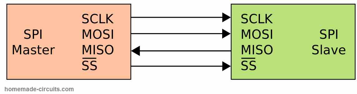
SPI protocol is single master multi-slave protocol, meaning there will be only one master device and may have two or more slave devices. SPI is also known as a four-wire serial bus.
Interfacing SPI protocol:
Master & slave:

Multi-slave:

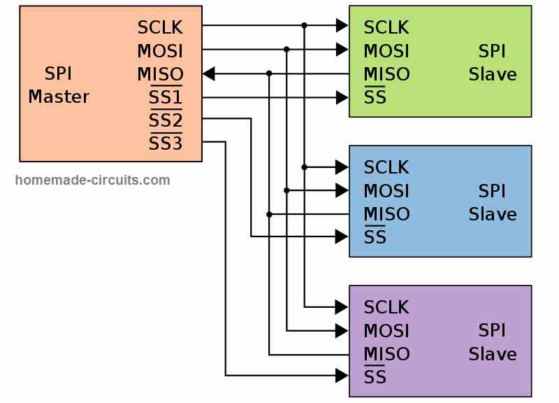
The SPI protocol needs four wires to interface and operate between master and slave device.
- SCLK – Serial clock – output from master device.
- MOSI – Master out slave in – data output from master device.
- MISO – Master in slave out – data input from salve device.
- SS / CS – slave select / chip select. The slave select is active low line and can be any general purpose I/O pin of a microcontroller.
Data transmission in SPI:
- To initiate SPI communication, the master starts to generate a clock signal that is compatible with the slave device, usually in the range of a few MHz.
- The next step is to pull the chip select line of the slave device to LOW. If there are multiple slave devices, the master device will pull down a particular slave’s chip select line.
- Now the master sends data via MOSI to slave and the slave responds to master via MISO. The slave devices whose lines are not pulled low must ignore the data and clock on the bus.
- Once the communication is completed the clock line will go idle.
Clock polarity & clock phase in SPI:
Whenever we write a program code for SPI communication we must mention the clock polarity and clock phase, only then proper communication gets established.
- Clock polarity or CPOL determines what will be the idle polarity state of clock line. When CPOL is set to 0, then the idle state of the clock line will be pulled down. When the CPOL is set to 1, the idle state of the clock line will be pulled up.
- Clock phase or CPHASE determines at which clock phase (rising edge or falling edge) of the clock signal, the transmitted data bit can be toggled (from HIGH to LOW or LOW to HIGH) and at which clock phase the transmitted data can be read by the receiver.
Timing diagram of SPI communication:

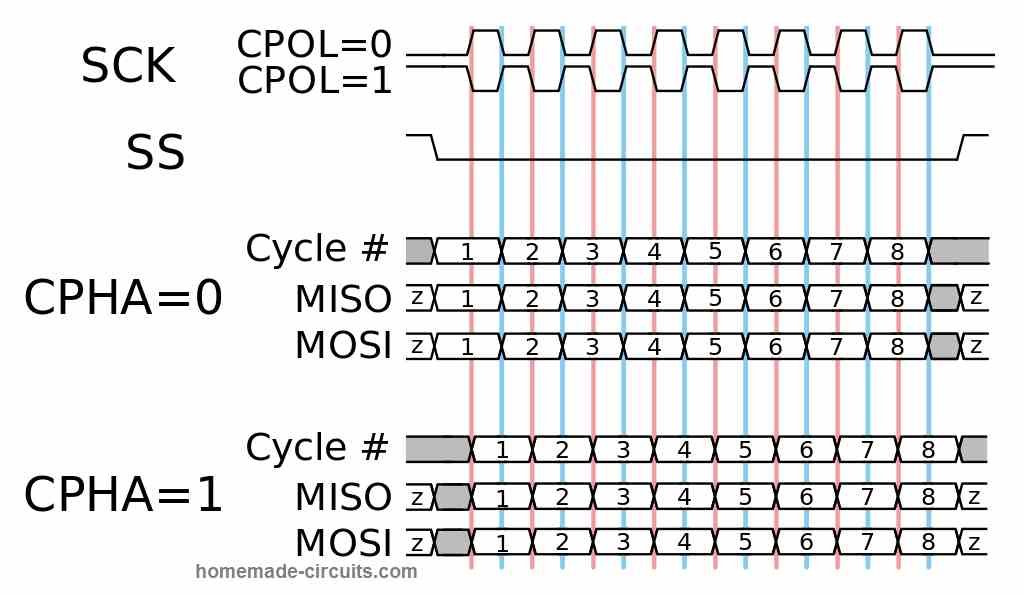
There are four modes of SPI communication:
Please refer to the above timing diagram while reading the explanation given below.
- CPOL = 0 & CPHASE = 0:
MODE 0: When CPOL is set to 0, the idle state of the clock is LOW and when CPHASE (CPHA) is set to 0, the data will be read when the clock is at rising edge and the data bit is allowed to change when the clock is falling edge.
- CPOL = 0 & CPAHSE = 1
MODE 1: When CPOL is set to 0, the idle clock state is LOW and when CPHASE (CPHA) is set to 1, the data will be read when the clock is at falling edge and the data bit is allowed to change when the clock at rising edge.
- CPOL = 1 & CPAHSE = 0
MODE 2: When CPOL is set to 1, the idle clock state is HIGH and when CPHASE (CPHA) is set to 0, the data will be read when the clock is at falling edge and the data bit is allowed to change when the clock at rising edge.
- CPOL = 1 & CPAHSE = 1
MODE 3: When CPOL is set to 1, the idle clock state is HIGH and when CPHASE (CPHA) is set to 1, the data will be read when the clock is at rising edge and the data bit is allowed to change when the clock is at falling edge.
This concludes SPI communication protocol.
CAN protocol:
CAN stands for controller area network, developed by Robert Bosch in 1983 and released in 1986 at Society of Automotive Engineers, Michigan, USA.
CAN protocol was developed for automotive vehicles to simplify communication between various sensors, drivers and peripherals etc. CAN is a multi-master bus and there are no slave devices and all nodes act as a master.
It sends and receives data serially and the mode of communication is half duplex and asynchronous. Since the communication is asynchronous the bit rate of the all CAN devices must be the same in a bus.
CAN is also a message broadcast system, meaning the data send over CAN bus is not targeted (from device A to device B like I2C or SPI), instead the broadcasted data will be read by all CAN devices and if the sent data is relevant to a CAN device it will process the data further and other CAN devices simply disregard the information.
Unlike I2C where a device address exists, CAN devices do not have a device address but it has an identifier.
Identifier conveys how important the message is (priority) and also used for arbitration management when multiple CAN devices start to communicate on the bus simultaneously.
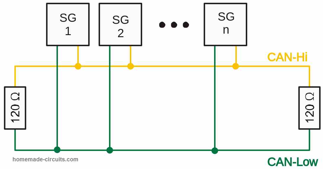
Hardware and electrical specification of CAN protocol:
CAN is a two wire protocol, its wires are twisted pair and unshielded. The two ends of the bus are terminated with 120 ohm resistors. The two wires of CAN bus are CAN HIGH and CAN LOW.

The communication protocols that I have explained previously uses HIGH and LOW for Logic ‘1’ and Logic ‘0’ respectively, but in CAN protocol we will be using differential voltage of the bus to send logic ‘1’ and logic ‘0’ (voltage difference between CAN HIGH and CAN LOW). This can be understood by using the illustrate graph:

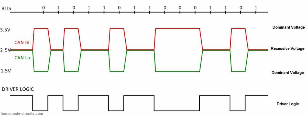
- In CAN protocol LOGIC ‘1’ is called recessive and LOGIC ‘0’ is called dominant.
- The bus is said to be logic ‘1’ or recessive when the CANH and CANL is applied with 2.5V and the differential voltage of these two lines are 0V.
- The bus is said to be logic ‘0’ or dominant when the CANH is pulled to 3.5V and CANL pulled to 1.5V and the differential voltage between the lines is 2V, this is how bits are transmitted through a CAN bus.
- When one of the CAN devices drives the bus dominant, it would be electrically impossible for the other CAN devices to drive the same bus to recessive.
Data frame of standard CAN bus:

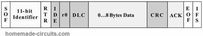

- The start of the frame is a single dominant (0) bit.
- The next part is identifier, which signifies the priority of the message which is 11 bit wide. A “stuff bit” is included in the identifier to maintain synchronization; the receiver will de-stuff or remove the synchronization bit.
- RTR – Remote transmission request signifies whether the data is for broadcasting or requesting information from other CAN device(s). Recessive (1) is sent when a CAN device is requesting data and dominant (0) is sent when broadcasting data.
- IDE – Identifier extension, 1-bit in length, must be the dominant bit for an 11 bit identifier data frame.
- r0 –Reserved bit for future improvement, must be a dominant bit.
- DLC – Data length code, 4-bit wide contains information about how many bytes of data is being sent.
- Data – The actual information in the frame to be received by other CAN devices. Up to 64 bits may be transmitted.
- CRC – cyclic redundancy check for checking data errors, 16 bit wide.
- ACK – Acknowledgement 2 bits wide. When a receiving CAN device gets the message accurately, the receiver writes this bit as dominant (0); if this bit is left recessive (it happens when receiving devices did not get correct data bits) the sender will resend the data again. Another bit in ACK is delimiter and it must be recessive.
- EOF – End of frame – 7 bit wide, all bits must be recessive.
- IFS – Inter frame space, 3-bit wide for delay between current and next frame, so that received devices can process the data.
Extended data frame for CAN bus:

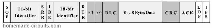
If we are using the extended CAN data frame, here are the differences:
- SRR – substitute remote request, must be a recessive bit.
- IDE must be a recessive bit to signify that this is an extended data frame.
- r1 – additional reserve bit.
Remote frame:
Remote frame is same as standard data frame but there are two differences:
- The RTR bit is set as recessive.
- There will be no data frame.
The purpose of the remote frame is to request data from other CAN device(s) on the same bus.
Arbitration:
When multiple CAN devices try to access the bus there will be collusion, to avert such data errors in the bus, arbitration is established. In CAN bus the device with highest priority wins the arbitration.
A device sending the identifier as “00000000001” will be given high priority compare to a device sending “00000000100” because device with identifier “00000000001” driven the bus with dominant bits (0) longer than the other. The device(s) lost the arbitration will retry when the bus is not busy.
In real world the identifiers in automotive vehicle equipment like airbag or transmission or ABS will be more prioritized than a music system or air conditioner. This concludes the basics CAN protocol.