In this post we'll discuss how to convert any ordinary square wave H-bridge inverter into an almost pure sine wave inverter circuit.
Basic Concept
The idea is simple, just chop the low side MOSFET gates of the H-Bridge with reverse SPWM (Sinusoidal Pulse Width Modulation) waveform. This will force the low side 50 Hz, or the 60 Hz signal at the MOSFET gates to get chopped into the corresponding SPWM waveform.
This Waveform will be correspondingly replicated across the output load causing the load to operate with this SPWM waveform. Since the SPWM is equivalent to a sinusoidal waveform, the output of the inverter will be transformed into a sine waveform. A calculated high voltage capacitor added across the inverter output will further enhance the SPWM waveform into a real looking sinusoidal waveform.
If you do not want to read the whole article, you can watch this video instead:

Universal Design
The diagram below shows a universal H-bridge sine wave inverter layout which can be applied to convert any square wave H-bridge inverter into a sine wave H-bridge inverter.
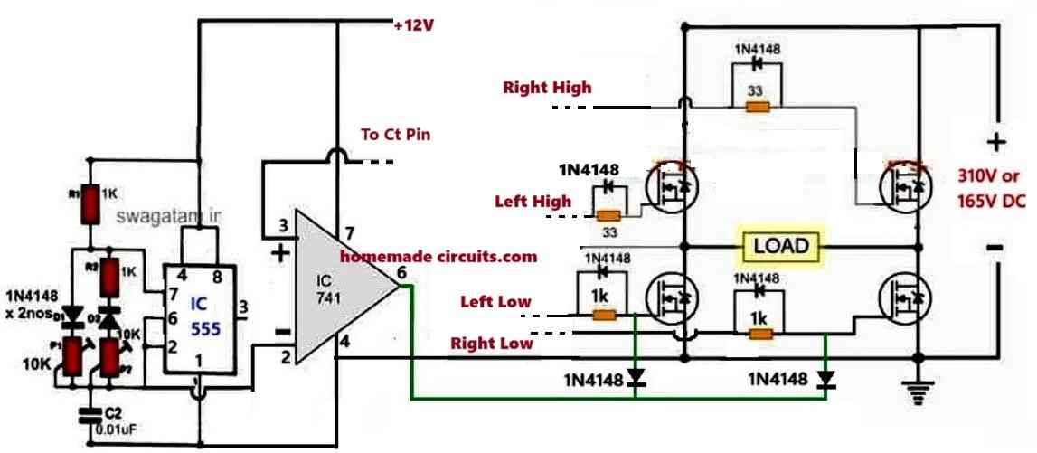
On the right hand side we see the H-bridge MOSFET stage using 4 N-channel MOSFETs. However, virtually all variants will work as long as the low side devices are N-channel.
Since we are only interested in the low side MOSFETs, the upper high side MOSFETs are irrelevant and can be ignored.
Operating the upper MOSFETs with SPWM is not necessary and is not required, because in an H-bridge topology the high side and low side MOSFETs operate in series, so switching any one of these with the SPWM is sufficient for the intended results.
Moreover, in H-bridge designs, that have 4 N-channel MOSFETs, the high side MOSFETs are operated using bootstrapping mechanism, which makes feeding an SPWM too complicated, and also an overkill.
Coming back to our universal H-bridge sine wave inverter design, the left side consists of two IC stages: IC 555 astable stage and an op amp IC 741 comparator stage.
The comparator op amp 741 or any standard op amp performs the main function of an SPWM generator.
It is rigged as a comparator to compare a couple of triangle waves fed across its inverting input pin#2 and the non-inverting input pin#3.
The non-inverting input pin#3 is fed with slow triangle waves, while the inverting input pin#2 receives a relatively fast triangle wave supply.
The op amp compares the two input exponential waveforms which results in the generation of the corresponding sets of SPWM waveforms at its output pin#6.
The slow triangle waves are derived directly from the inverter's existing H-bridge oscillator IC, across its timing capacitor Ct. This Ct timing capacitor is available in all inverter designs regardless of the topology.
The slow triangle waveform across the Ct pin of the inverter IC actually determines the output 50 Hz or the 60 Hz frequency of the inverter. Therefore, by using this waveform as this slow triangle waves we get two advantages: firstly it helps to carve out the intended SPWMs, and secondly it perfectly synchronizes the SPWM with the main inverter frequency, enabling the inverter output sine waveform to be precisely in sync with the 50 Hz / 60 Hz ON/OFF timing.
The fast triangle waves are extracted from across the timing capacitor of the IC 555 astable C2. The fast triangle waves decide the frequency of each SPWM waveform, which must not exceed 300 Hz if the inverter transformer is an iron core transformer.
If the transformer is a ferrite cored transformer, then you can increase the fast triangle wave frequency to any higher limit, as suitable.
Higher the frequency of the SPWM, higher will be the efficiency of the output sine wave.
The presets P1, P2 can be used to tweak the SPWM so that it replicates an output sine waveform as close as possible to an original sinusoidal waveform.
The SPWM output waveform from the op amp IC 741 is finally applied to the gates of the low side H-Bridge MOSFETs via individual 1N4148 diodes.
You can see in the diagram, the 1N4148 diodes are reverse biased, meaning the chopping of the 50 Hz or the 60 Hz waveform at the MOSFET gates will be only through the negative pulses of the SPWM, the positive pulses have no effect.
This configuration will allow the low MOSFETs to switch exactly as per the switching of the SPWM waveform from the IC 741 output, generating the required sine wave AC output for the connected.
In this way any ordinary H-bridge inverter circuit can be transformed into a pure sine wave H-bridge inverter circuit.
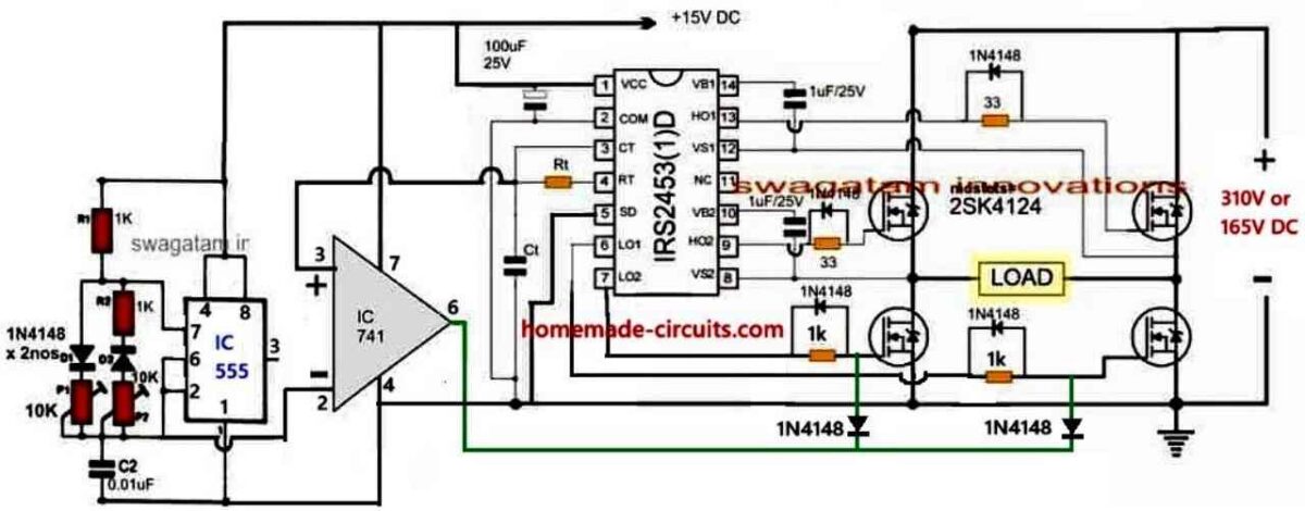
A Practical Sine wave Inverter Design
The following diagram shows a practical example of how an simple IRS2453 H-bridge inverter circuit can be converted into a sine wave H-Bridge inverter circuit.
For any further questions or doubts, please feel free to comment below to get quick replies from me.
thank you for your time and support electronics services Engineering
best regards
Ebrahim Sabeer.
You are welcome Ebrahim!
Hello, can this system be used for a heater to what extent? At the moment I have a tank type for a 300 l heat pump with a double coil, a 3 kW heater. Powered by 9 panels of 410 W, the AZO 4 kW converter is great. My question is the converter system designed by you. Can it be used. In my opinion, whether the increase in frequency will be correct, and the rectangular waveform. I have a request for an answer to my question. Possibly suggest what converter system should be used. I am full of admiration for your projects. Best regards from Poland.
Thank you very much for your question!
For a resistive heater you can use a standard square wave voltage or even a DC voltage, the waveform is not critical.
While the above design sine wave design can be used for resistive heater devices, it is not necessary.
You can simply use any standard square wave inverter circuit.
If you have any further questions please feel free to ask…
hello sir , i am working on solar H-bridge inverter 5000 watt i am using 40 mosfets of irfp460, 10 on each side i connected them on good heat sink with coolar i have 3 question number one if i using tl494 ic to drive mosfets it is good?because i found it easy to make Oscillator circuit…..?
question number two what is the best resistor to but on the gate every mosfet to run it good?
question number 3 the amount of this mosfet it is good to run this inverter?
thank you for your kind for helping beginners……
Hello happy dude2004,
TL494 is not good because it will not allow you to get 50Hz or 60Hz frequency, and it is not an H-bridge driver IC
If you want to build an H-bridge inverter you can try the last circuit explained in the above article.
Resistor will depend on frequency, but any values between 10 ohm and 50 ohm will mostly work. Connect just one resistor to the parallel gate output of the MOSFETs.
10 parallel MOSFETs on each channel should be ok, considering each MOSFET is rated to handle 20 amps.
i want to thank you for your reply .
the is on this article is not available at any store on my country but i have two ic SG3524 and SG3525 both can work instead of tl494 ??
and solution of gate mosfet i put resistor (10 ohm and 50 ohm ) on every gate of mosfets or connect one resistor for all gates mosfet ?
and thanks again
SG3524 and SG3525 cannot be directly used to build an H-Bridge inverter, that is why I am not recommending it.
There’s is one way to solve the H-bridge issue, by using P-channel MOSFETs for the high-side MOSFETs.
But for this, the supply DC input to the MOSFET drain will need to be same as the Dc which is used for the IC Vcc.
A single gate resistor can be used for each parallel set of MOSFETs.
Hello, good afternoon, my name is Carlos from Argentina, I am a faithful follower of the website. In this case I want to ask you if you have or can build a circuit for laboratory variable sources to set the output voltage…. Example: when you set a voltage and then activate the circuit to lock said voltage… Even if the potentiometer no matter how the tension moves, it is fixed, This is to avoid any accidental movement of the potentiometer and burning any circuit under test. From already thank you very much.
Thank you Carlos, for being a regular visitor of this blog.
However, sorry, i don’t seem to have the circuit for locking a power supply voltage, as set by the pot.
If possible I will try to figure out an appropriate design and let you know soon.
I want to try this circuit with 555 and 741, can I substitute 741 for a lm386, I have a few of these if not I will order some thanks
LM386 is an audio amplifier IC, but I guess it can be also used like an opamp or comparator.
You can try it and check the SPWM response, if you find it appropriate then it may be fine to use it…
I have one, it’s not one of them fancy ones, it’s a first DSO-152. Seems to get the job done and it still works. Yes, an o-scope is a must if you want to build inverters. Thanks for the knowledge. Whenever I get time I always go to your website to learn new things.
You are most welcome Art, all the best to you!
See I am still learning, thanks. When I build and get ready to apply power, only two things can happen, it works or it blows up.
You must verify the square wave inverter and the SPWM stage circuits separately, if they work correctly only then integrate them together.
You will need an oscilloscope for verifying the waveforms.
my greetings to you sir,swag.
I am very much interested to this topic.
Thank you Kenneth,
Let me know if you have any related questions.
From what I know you need a fundamental square wave at 50 or 60 ha, and a SPWM wave at a much higher feuq.and the h- bridge combines them for a digital sign wave then Lc circuit to get the final wave form. My SPWM circuit was to far away from the mosfets and keep blowing them up and everything else. Funny three years ago I never heard of a h- bridge, boost converter and many other things when it comes to building a inverter, I was old school just get a very big transformer and start there. I have learned a lot from your web site. Thank you for the knowledge.
Thank you for your feedback, Not square wave, you need a fundamental triangle wave or a sine wave at 50 or 60 Hz.
You know I was interested in the 555 and the 741 combo circuit. You brought it to my attention again. You seem to know a lot about inverter circuits. These big companies that build 5000 8000 or more watts are using many boost converters in parallel. I just finished up on a two transformer 2000 watt boost converter, I think I will give your 555 and the 741 a try. Some where I need to fit a totem pole to drive the MOSFET or maybe use IGBT they don’t seem as fragile as the MOSFET. Thanks for bringing this circuit back up.
Thank you for your kind feedback, yes you can use the 741, 555 circuit to generate SPWM, to convert square wave inverter to sine wave.
This is a quiet good job Sir.But the output of IC 555 is not connected. That is my observation, and I want to know the reason.
Thank you Ayodele,
The 555 astable is used as a triangle wave generator, not as a square wave generator. The triangle waves are obtained from pin6/2 of the IC.
Pin#3 output is unused in this application.
Mgr.Engineer,it is possible in Urdu translate or language?
Yes you can translate in English and post the question here.