The IC UC3854, what it does is, it helps in active power factor correction, right? Now normally, if we don’t correct the power factor, then power system will pull current from the AC mains in a way that’s not a nice sine wave but rather distorted. This IC takes care of all the control stuff needed to make sure the power supply uses the available current properly while also keeping the current waveform as clean as possible.
Basic Working
Now inside this IC we have many important building blocks. There’s a voltage amplifier, then an analog multiplier and divider, a current amplifier and a PWM that runs at a fixed frequency.
We also have a gate driver that works well with power MOSFETs, then a 7.5V reference, something called a line anticipator, a load-enable comparator, a low-supply detector, and an overcurrent comparator.
So this IC works using something called average current-mode control. That means it controls the current in such a way that keeps the frequency fixed but also makes sure the system stays stable and the distortion stays low.
Now if we compare this with peak current-mode control, then average type looks better because it keeps the input current waveform properly sinusoidal without needing slope compensation and without being too sensitive to noise spikes.
This IC has a high reference voltage and a strong oscillator signal so it doesn’t get easily affected by noise. Also because it has fast PWM circuitry, it can work at switching frequencies above 200kHz which is quite high.
Now We can use it in both single-phase and three-phase systems and it can handle input voltages from 75V to 275V, while also working with AC line frequencies anywhere from 50Hz up to 400Hz.
Another nice feature is that when the IC starts up, it doesn’t draw much power, so the power supply feeding it doesn’t get overloaded.

When it comes to packaging, this IC comes in 16-pin plastic and ceramic DIP (dual in-line package) versions and there are also surface-mount options available. So overall, a pretty useful IC for making power factor correction work properly!
Detailed Description
This UC3854 IC helps us do active power factor correction in systems where otherwise, we would have a non-sinusoidal current being drawn from a sinusoidal power line. So this IC makes sure that the system pulls power from the line in the best possible way while keeping line current distortion as low as possible, ok?
To achieve this, we have average current mode control inside this IC, and what this does is, it keeps the current control fixed-frequency but at the same time, it also ensures good stability and low distortion.
The good thing about average current mode control is that it lets the boost stage move between continuous mode and discontinuous mode without causing any performance issues.
But if we had used peak current mode then we would need slope compensation and still it would not be able to maintain a perfect sinusoidal line current. Plus peak current mode tends to react more to noise transients but average current mode does not get affected much, ok?
Now this UC3854 IC has everything inside it that we need to make a power supply that can extract current optimally from the power line while keeping line current distortion to a minimum.
So here we have a voltage amplifier, an analog multiplier and divider, a current amplifier, and also a fixed-frequency PWM all inside this single IC.
But wait, this IC also has a gate driver that is fully compatible with power MOSFETs, a 7.5V reference, a line anticipator, a load-enable comparator, a low-supply detector and an overcurrent comparator.
So everything that we need for active power factor correction is already inside, making this IC super useful for designing efficient power supplies.
This UC3854 IC has all the circuits inside that we need to control a power factor corrector, right? Now this IC is mainly designed to work with average current mode control but the good thing is we can also use it with different power topologies and control methods if we want. So, it is quite flexible.
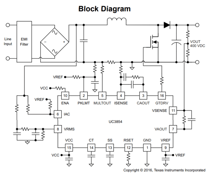
Block Diagram
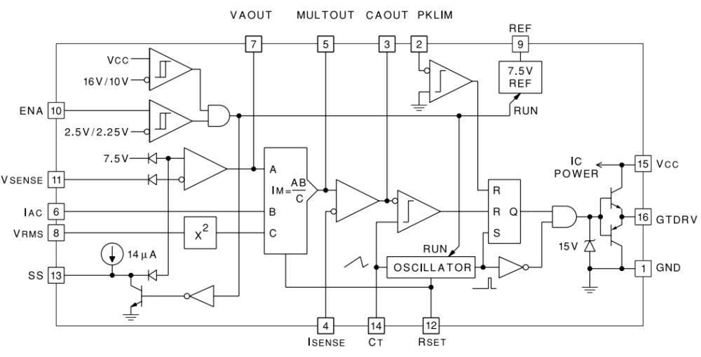
Under-Voltage Lockout and Enable Comparators
If we look at the block diagram, in the top left corner, we see two important things—the under-voltage lockout comparator and the enable comparator. These two must both be in the "true" state for the IC to start working, ok?
Voltage Error Amplifier and Soft-Start Function
Then we have the voltage error amplifier whose inverting input goes to pin VSENSE. Now in the diagram, we see some diodes around the voltage error amplifier but these diodes are just there to help us understand how the internal circuits work. They are not actual diodes inside.
Now what about the non-inverting input of the error amplifier? It normally connects to a 7.5V DC reference but it is also used for soft-start.
So what happens is, when the circuit starts, this setup lets the voltage control loop begin working before the output voltage reaches its final level.
This way we do not get that annoying turn-on overshoot that many power supplies have.
Then there is another ideal diode in the diagram between VSENSE and the inverting input of the error amplifier but it is just there to clear any confusion—there is no extra diode drop in the actual circuit. Instead, inside the IC we do all this using differential amplifiers. Also, we have an internal current source to charge the soft-start timing capacitor.
Multiplier Functionality
Now let us talk about the multiplier. The output of the voltage error amplifier is available on pin VAOUT and this is also one of the inputs to the multiplier.
Another input to the multiplier is IAC, which comes from the input rectifiers and helps program the wave shape. This IAC pin is internally held at 6V and acts as a current input.
Then we have VFF which is the feedforward input and inside the IC its value gets squared before going to the divider input of the multiplier.
Another thing that goes into the multiplier is ISET which comes from pin RSET, and it helps set the maximum output current.
Now what comes out of the multiplier? The IMO current which flows from pin MULTOUT and this connects to the non-inverting input of the current error amplifier.
Current Control and Pulse Width Modulation
Now the inverting input of the current amplifier is connected to pin ISENSE and its output goes to the PWM comparator, where it gets compared with the oscillator ramp signal from pin CT.
The oscillator and comparator then control the set-reset flip-flop which in turn drives the high-current output at pin GTDRV.
Now to protect the power MOSFETs, the output voltage of the IC is clamped internally to 15V, so we do not end up overdriving the MOSFET gates.
Peak Current Limit and Power Supply Connections
For safety, there is an emergency peak current limit function which is controlled by pin PKLMT. If this pin is pulled slightly below ground, then output pulse shuts off immediately.
Finally we have the reference voltage output on pin VREF and the input voltage goes to pin VCC.
Application Information
Ok, so this IC is mainly used in AC-DC power supplies where we need Active Power Factor Correction (PFC) from a universal AC line. That means we can use it in systems where the input voltage can vary widely but we still need to make sure that the power factor stays high and the input current harmonics stay low, ok?
Now applications that use this UC3854 IC usually follow the Class D equipment input current harmonics standards, which is part of EN61000-3-2.
This is an important standard for power supplies that have a rated power above 75W so if we are designing something like that, then this IC helps us meet those harmonic distortion limits without extra hassle.
If we check the performance of this IC in a 250W power factor correction circuit, then we can see it has been properly tested using a precision PFC and THD measuring instrument.
The results? Power factor was 0.999 which is almost perfect and Total Harmonic Distortion (THD) was just 3.81%. These values were measured up to the 50th harmonic of the line frequency, at nominal input voltage and full load. So this tells us that this IC can really help us get a clean and efficient power conversion.
Typical Application (PFC Circuit Diagram)
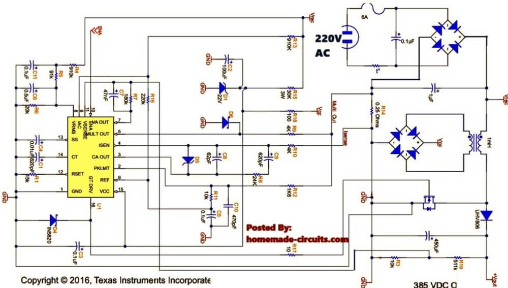
If we look at Figure above, we see a typical application circuit where the UC3854 IC is used as a preregulator with high power factor and high efficiency.
So how is this built? We have two main sections in this circuit:
- The control circuit which is built around the UC3854.
- The power section which actually handles the power conversion.
Now the power section here is a boost converter and the inductor inside it works in continuous conduction mode (CCM).
What this means is that the duty cycle will depend on the ratio of the input voltage to the output voltage, ok? But the good thing is, because the inductor is working in continuous mode, so the input current ripple at the switching frequency stays low.
This means that we get less noise on the power line which is important for EMI compliance.
Now one important thing in this circuit is, the output voltage must always be higher than the peak voltage of the highest expected AC input voltage. So we need to select all the components carefully making sure they can handle the voltage ratings without any issue.
At full load, this preregulator circuit achieves a power factor of 0.99, no matter what the input power line voltage is, as long as it stays between 80V to 260V RMS. That means that even if the input voltage changes, the circuit still corrects the power factor effectively.
Now if you need a higher power level, then you can still use this same circuit but you might have to make small changes to the power stage. So you do not need to redesign everything from scratch, just tweak a few things to handle the higher power requirements.
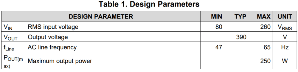
Design Requirements
For the above shown PFC circuit design example, we will use the parameters as indicated in the following Table 1 as the input parameters.
Comprehensive Design Process
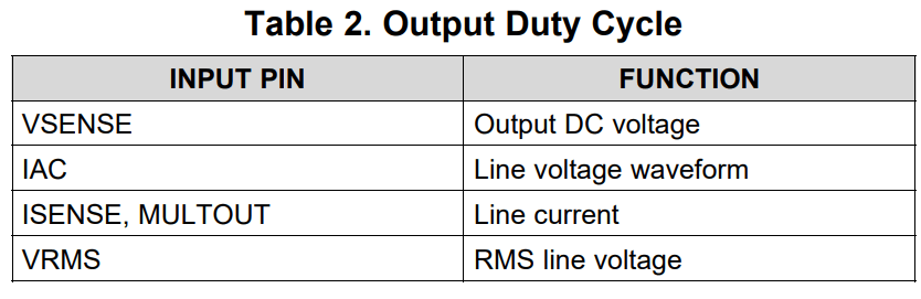
The power MOSFET gate in the control stage of the circuit receives the PWM pulses (GTDRV) from the UC3854. Four different inputs to the chip work together to concurrently regulate the duty cycle of this output.
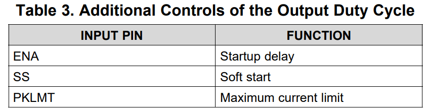
Added controls of an auxiliary type are offered in this design. They serve as a safeguard against specific transient situations for the switching power MOSFETS.
Protection Inputs
Now we talk about the protection inputs in this IC. These are important because they help us control the circuit in case of problems, power-up delays, or overcurrent situations, ok.
ENA (Enable) Pin
Now, here we have the ENA pin which stands for Enable. This pin must reach 2.5 V before the VREF and GTDRV outputs can turn on. So it means we can use this pin to shut down the gate drive if something goes wrong or we can use it to delay the startup when the circuit first powers up.
But there is more. This pin has a hysteresis gap of 200 mV which helps prevent erratic switching or unwanted turn-ons due to noise. So once it crosses 2.5 V, it will stay on until the voltage drops below 2.3 V, making the operation more stable, ok.
We also have undervoltage protection inside the IC which directly works at VCC. The IC will turn on when VCC reaches 16 V and will turn off if VCC falls below 10 V. This means that if the power supply voltage drops too low, then IC will automatically shut down to prevent malfunction.
But if we are not using the ENA pin, then we must connect it to VCC using a 100 kilo-ohm resistor. Otherwise it might float and cause unwanted behavior.
SS (Soft Start) Pin
Next we move to the SS pin which stands for Soft Start. It controls how fast the circuit starts by reducing the reference voltage of the error amplifier during startup.
Normally if we leave the SS pin open then reference voltage stays at 7.5 V. But if we connect a capacitor CSS from SS to ground then the internal current source inside the IC will charge this capacitor slowly.
The charging current is about 14 milliamps so the capacitor charges linearly from 0 V to 7.5 V. The time it takes for this to happen is given by this formula.
Soft Start Time = 0.54 * CSS in microfarads seconds
This means that if we use a larger capacitor then startup time becomes longer, making the circuit turn on smoothly instead of suddenly jumping to full voltage, ok.
PKLMT (Peak Current Limit) Pin
Now we come to PKLMT which stands for Peak Current Limit. This pin is very important because it sets the maximum current that the power MOSFET is allowed to handle.
Let us say we use the resistor divider shown in circuit diagram. Here is what happens.
The voltage at PKLMT pin reaches 0 volts when the voltage drop across the current sense resistor is:
7.5 volts * 2 k / 10 k = 1.5 volts
If we use a 0.25 ohm current sense resistor, then this 1.5 volt drop corresponds to a current of:
Current I = 1.5 / 0.25 ohms = 6 amperes
So this means the maximum current is limited to 6 amperes, ok.
But one more thing. TI recommends that we connect a bypass capacitor from PKLMT to ground. Why. Because this helps filter out high-frequency noise, making sure the current limit detection works accurately and does not get affected by unwanted noise spikes.
Control Inputs
VSENSE (Output DC Voltage Sense)
Ok, now we talk about the VSENSE pin. This pin is used to sense the output DC voltage. The threshold voltage for this input is 7.5 volts, and the input bias current is typically 50 nanoamperes.
If we check the values in circuit diagram we see they are based on an output voltage of 400 volts DC. In this circuit, the voltage amplifier works with a constant low-frequency gain to keep output fluctuations minimal.
We also find a 47 nanofarad feedback capacitor which creates a 15 hertz pole in the voltage loop. Why do we need this? Because it prevents 120 hertz ripple from affecting the input current, making the operation more stable, ok.
IAC (Line Waveform)
Now let us move to the IAC pin. What does it do? It helps to make sure that the line current waveform follows the same shape as the line voltage.
So how does it work? A small sample of the power line voltage waveform is fed into this pin. Inside the IC, this signal is multiplied by the output of the voltage amplifier in the internal multiplier. The result is a reference signal used by the current control loop, ok.
But here is something important. This input is not a voltage input but a current input and that is why we call it IAC.
Now how do we set this current? We use a resistor divider with 220 kilo-ohms and 910 kilo-ohms. The voltage at the IAC pin is internally fixed at 6 volts. So these resistors are chosen in such a way that the current flowing into IAC starts from zero at every zero crossing and reaches about 400 microamperes at the peak of the waveform.
We use the following formulas to calculate these resistor values:
RAC = VPK / IACPK
which gives us
RAC = (260 volts AC * √2) / 400 microamperes = 910 kilo-ohms
where VPK is the peak line voltage.
Now, we calculate RREF using:
RREF = RAC / 4
so, RREF = 220 kilo-ohms
ISENSE and MULTOUT (Line Current)
Ok, so here the voltage drop across that 0.25 ohm current-sense resistor is applied to ISENSE and MULTOUT, like shown in the circuit. Now this current-sense amplifier, it is designed to work with high low-frequency gain but we got to know one thing—it is not the same as the voltage amplifier.
Why? Because here this current-sense amplifier is made so that the current-control loop gets very wide bandwidth. So what does this do? Simple—it helps the line current follow the line voltage as close as possible.
Now in this case, this amplifier has something called a zero at about 500 hertz and after that the gain increases by about 18 decibels. That means after 500 hertz, the amplifier really starts boosting the signal in a way that helps maintain proper current tracking.
VRMS (RMS Line Voltage)
Here is one big advantage of the UC3854 preregulator. It is made in such a way that it can handle a very wide range of input voltages. We are talking about everything from as low as 85 volts AC (like in the US) to as high as 255 volts AC (like in Europe).
But how does it do this? Well, this IC uses something called line feedforward. What is that? Ok, this thing helps to keep the input power constant no matter if the input voltage goes up or down. But—it only works if the load power stays constant.
Now inside this IC, we got a multiplier circuit. And this multiplier does something very specific—it divides the line current by the square of the RMS value of the line voltage.
Here is how it works:
The voltage applied to the VRMS pin is proportional to the average of the rectified line voltage and also to the RMS value of that voltage.
Inside the UC3854, this voltage is squared and then used as a divisor in the multiplier block.
The output of this multiplier which we get at MULTOUT, is a current. Now this current increases if the IAC current increases and if the VAOUT voltage increases. But it decreases if the VRMS voltage increases.
So basically, as the input voltage increases, the multiplier works in a way that keeps everything balanced.
PWM Frequency
Now if we look at the circuit diagram, we see the PWM oscillator frequency in this circuit is set at 100 kilohertz. But how is this frequency decided? Well, it depends on two components—CT capacitor at CT pin and RSET resistor at RSET pin.
We must select RSET first because this resistor affects the maximum value of IMULT which is given by this equation:
IMULTMAX = -3.75 V / RSET
Lets take an example. If we select:
RSET = 15 kilo-ohms then we get:
IMULTMAX = -3.75 V / 15 kΩ = -250 µA
So this means the maximum current coming from the multiplier output is 250 microamperes in the negative direction.
One very important thing to note—the multiplier output current never goes above twice the IAC current. So we got to keep that in mind while designing.
Current Limit Calculation
Now let us say we connect a 4 kilo-ohm resistor from MULTOUT to the 0.25 ohm current-sense resistor. Then, what happens?
We calculate the maximum current in the current-sense resistor using this equation:
IMAX = (-IMULTMAX × 4 kΩ) / 0.25 Ω
Now if we substitute the values then we get:
IMAX = -4 A
Which means, at the maximum this resistor will see 4 amperes of current flowing through it in the negative direction.
Capacitor CT Calculation
Alright, now that we have selected RSET, the current sense resistor and the resistor from MULTOUT to the current sense resistor, the next step is to calculate CT for the desired PWM oscillator frequency.
For this we use this simple formula:
CT = 1.25 / (F × RSET)
where F is the PWM frequency in hertz.
So once we pick the right values for F and RSET then we can determine what capacitor value to use for CT to get the required switching frequency.
Need Help? Please Leave a Comment! We value your input—Kindly keep it relevant to the above topic!