In this article I have explained comprehensively regarding how to design a sine wave inverter without any form of coding or complex circuit designs. The included designs are simple yet extremely precise with their sine waveform structure.
You might have often felt discouraged, thinking that making a sine wave inverter from the scratch can be too complex, when in reality, it is not.
We will try to understand the procedures in the following paragraphs.
What is Sine Wave Inverter
A sine wave inverter is a device which converts battery power into a 220 V AC or a 120 V AC sine wave output.
There are 3 basic types of inverters: square wave inverter, modified sine wave inverter and a pure sine wave inverter.
The voltage waveform output from a square wave inverter is square wave. The main drawback of a square wave inverter is that they cannot be used to operate electronic gadgets or sophisticated home appliances.
The voltage waveform output from a modified inverter is optimized to produce a modified square wave which is closer to a sine wave but not a pure sine wave. These inverters can be used to operate some selected home appliances or electronic gadgets, not all.
The voltage output from a pure sine wave inverter is a pure sine wave which has properties exactly similar to our mains AC waveform. And therefore these inverters become suitable for operating almost all of the home appliances without any concerns.
How does a Basic Pure Sine Wave Inverter Works
A pure sine inverter works by inducing an alternating sine waveform pattern across the primary transformer winding with a selected frequency rate. This frequency rate can be 50 Hz or 60 Hz, depending on the country and region specifications.
This sine waveform is in the form of sine PWM which is a digital signal and not a linear signal. Because inverters use power transistors which cannot be efficiently operated using a linear signal.
Using a linear signal can make the transistors very hot and inefficient. That is why we employ digital PWM which ensures efficient operation of the transistors with minimum heat generation.
This sine waveform are generated using SPWM or sine PWM. An ordinary PWM refers to pulse width modulation signal whose pulse width is adjusted at a certain fixed specified width. However, in a sine PWM, the pulse widths are adjusted with a varying widths, so that its average voltage pattern interprets into a linearly varying, exponential sine waveform at the output of the transformer.
A transformer being an analogue inductive device is able to effectively process the digital SPWM oscillations into an exponentially varying pure sine waveform at its output.
Basically, we manufacture the SPWM waveform through an op amp IC or an IC 555 and force the inverter MOSFETs to oscillate in accordance with this SPWM pattern. The MOSFETs then in turn induce the same SPWM pattern across the transformer primary winding to generate a pure sine wave AC at the secondary output of the transformer.
Designing a Sine Wave Inverter - Prerequisites
To design a pure sine wave inverter from the scratch, we require the following circuit stages:
A basic 50 Hz or 60 Hz inverter circuit.
An op amp comparator using IC 741 or by configuring IC 555.
Two sets of triangle waveform, one slow (low frequency) and the other fast (high frequency).
The slow triangle wave must be synchronized with the 50 Hz or 60 Hz base frequency of the main inverter oscillator.
The synchronization is essential to ensure that the set of SPWM waveform fits correctly inside each alternating signal from the 50 Hz oscillator.
Generating Synchronized SPWM
For generating our SPWM we use an op amp based comparator circuit as shown in the following diagram:
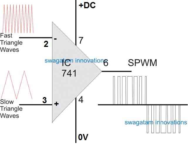
It is a simple op amp comparator which compares the varying voltage levels of the slow triangle wave against the fast triangle waves and produces the resultant SPWM.
Please note that, ideally the slow triangle wave must be actually a slow sine wave. However, creating a sine wave can be a little complex, therefore we use a slow triangle wave as a crude replacement for the sine wave.
At the output of the op amp you can see the SPWM pattern generated after comparing the two triangle waves across the op amp inputs.
The SPWM pattern is basically a digital PWM representation or replication of the analogue slow triangle wave.
Have a closer look at the SPWM pulse width distribution. You can see that it has widely separated thin pulse widths at the outer sides of the waveform, while the center section is concentrated with proportionately incrementing, closely positioned, wider pulse widths.
The outer thinly populated pulse widths are equivalent to the exponentially rising and falling waveform sections of a sine wave cycle, while the thickly populated central SPWMs replicate the peak voltage section of the analogue sine wave cycle.
The period or the length of the SPWM set is same as the period or the length of the slow triangle wave. The frequency or the number of pillars inside the SPWM waveform cycle is same as the number of fast triangle waves which can accommodate inside every single slow triangle wave cycle.
The greater the number of pillars inside the SPWM, the higher the sine wave purity at the inverter output, and vice versa.
Thus in order to get the purest possible sine wave at the inverter output you can consider having an optimally high frequency for the fast triangle waves.
Now, the best way to extract these triangle waves is from oscillator circuits or astables which have an exclusive RC timing network.
So the triangle wave can be extracted from right across the "C" or the capacitor of the RC network.
Let's take the example of our very old IC 555 astable circuit. You can extract the fast triangle waves from across the timing capacitor of the IC.
Smaller capacitor values will give faster triangle waves and vice versa.
So this takes care of the fast triangle waves, what about the slow triangle waves? The slow triangle wave which must be ideally a sine wave is very crucial as this must be synchronized with the 50 Hz or 60 Hz cycles of the main square wave inverter.
The slow triangle wave must be synchronized with your main inverter because it is essential that the length of each SPWM set fits perfectly inside each 50 hz square wave cycle operating the power MOSFETs. Otherwise the sine wave at the output of the inverter will not be uniform, rather be in a haphazard form.
Fortunately, this synchronized slow triangle wave can be extracted from across the timing capacitor (Ct) of the main inverter oscillator circuit.
Here, each slow triangle wave corresponds to each square wave signal at the output of the oscillator circuit. Due to this property this slow triangle wave becomes suitable as the synchronized slow triangle.
Using IC 555 for Generating SPWM
Since IC 555 also has built-in op amps, it can be also effectively used to process SPWM waveform. The basic circuit diagram is shown in the following figure:
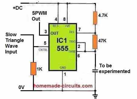
Here, we configure the IC 555 as an astable circuit and use its pin#5 control input to modulate the astable frequency for generating the required SPWM output at pin#3.
Integrating SPWM with the MOSFETs
From the above discussions we understood that the slow triangle waves can be extracted from across the timing capacitor of the main inverter oscillator IC, and the fast triangle wave can be extracted similarly from across the timing capacitor of a separate free running oscillator circuit.
Once the above aspects are implemented across the op amp comparator inputs, the intended SPWM can be acquired from the output of the op amp.
Next, it is crucial to integrate this SPWM with the inverter, so that the inverter becomes customized to generate a pure sine wave at the output of the transformer.
To implement this you just have to create and configure the BJT/MOSFET stage as shown below:
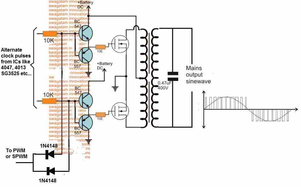
As shown in the above figure, a couple of NPN/PNP BJT pairs are arranged in the form of totem pole network to switch the MOSFETs efficiently. Since these BJTs have high value base resistors it becomes ideal to switch their bases with the SPWM without loading the comparator op amp.
Practical Examples
Now, since we have comprehensively learned regarding how to interface SPWM with a basic inverter, let's investigate a few practical examples for better understanding.
We will discuss 2 examples using IC 4047 and the IC 555.
Designing an IC 4047 Pure Sine Wave Inverter
The IC 4047 based inverter is a very popular design, since it allows the user to quickly build and implement the inverter circuit. However, the basic 4047 design produces a square wave output.
Nevertheless, using the SPWM interfacing method explained above, we can easily convert an IC 4047 based inverter into a pure sine wave inverter.
The complete circuit diagram can be witnessed in the following figure:
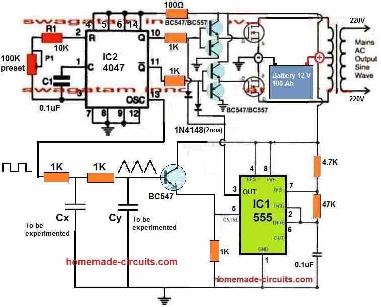
In the above 4047 inverter concept, we can see a practical implementation of SPWM using the IC 555.
Since we already have the pin#13 on IC 4047 which generates one clock pulse corresponding to each clock pulses at pin#10 and pin#11, it becomes perfectly suitable for SPWM synchronization purpose.
We first convert the pin#13 square waves into triangle waves using a double RC network, and feed the resultant triangle waves to a BJT emitter follower.
The BJT emitter follower makes the triangle waves stronger and more effective for processing at the control input pin#5 of the IC 555.
The op amps inside the IC 555 compare the slow triangle waves at pin#5 with the fast triangle waves at its pin#7 and generate the intended synchronized SPWM at its pin#3.
How to Calculate the Passive Integrator Cx and Cy Capacitor and the Resistor Values.
Formula:
The RC time constant relationship is:
fc = 1 / (2 * π * R * C)
R * C = 1 / (2 * π * fc)
For fc = 100 Hz:
R * C = 1 / (2 * π * 100) = 1592 * 10-6 seconds
Choosing Component Values:
First Stage (R1, Cx):
Choose R1 = 10 kOhms:
Cx = 1592 * 10-6 / (10 * 103) = 159.2 nF
Second Stage (R2, Cy):
Similarly, for the second stage:
R2 * Cy = 1592 * 10-6 seconds
Choose R2 = 10 k Ohms:
Cy = 1592 * 10-6 / (10 * 103) = 159.2 nF
Final Estimated Values to get a Reasonably good Sine Wave Output from the Integrator:
- R1 = 10 kOhms
- Cx = 159 nF (rounded to the nearest standard value)
- R2 = 10 kOhms
- Cy = 159 nF
Designing an IC 555 Pure Sine Wave Inverter Circuit
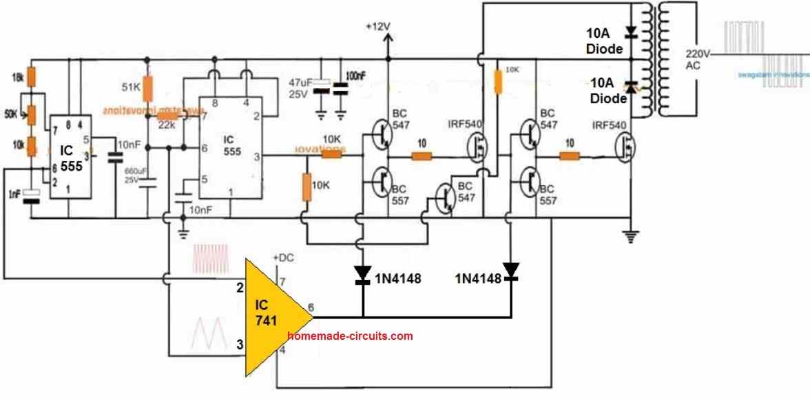
In the above setup the SPWM processor circuit is designed around an op amp.
As previously discussed, the slow triangle waves at pin#3 of the op amp are extracted from the main 555 inverter IC at the right side.
For the fast triangle waves we have configured a separate 555 astable at the extreme left side, which supplies the required fast triangle waves to the op amp comparator.
The resulting SPWM waveform is integrated to the bases of the BJT/MOSFET stage of the inverter.
Setting the SPWM Frequency
When you visualize the SPWM waveform, you find it to be having many verticals pillars or pulses. Although, higher number of pillars would contribute to more refined sine waveform, it would also cause heating up of the transformer, if the transformer is an iron core transformer.
The number of pulses inside each SPWM cycle defines the frequency of the SPWM.
Since mostly, our basic inverter would include an iron core transformer, optimizing the number of pulses on each SPWM waveform or the frequency of the SPWM is crucial. If this is too low, the sine waveform may not be perfectly formed, if the frequency is too high, the transformer may heat up.
The rule of thumb is to have around 5 pillars or 5 pulses on each SPWM cycle. Here's an example image of the SPWM we are recommending.

Since the number of pulses on each SPWM is determined by the fast triangle waves, the frequency of the fast triangle wave generator must be adjusted appropriately to get the above results.
How to Match the Transformer with the SPWM
Since we are chopping the 50 Hz or the 60 Hz base square wave frequency with our high frequency SPWM, this may cause the mean or the average voltage of the waveform to reduce drastically.
This means that the MOSFETs would switch the transformer primary with lower amount of current, causing a proportionately reduced voltage to be generated at the secondary side of the transformer.
In other words, suppose the battery voltage is 12 V, and transformer primary is 12-0-12V, then using square waves the transformer primary would be switched using the full battery 12 V.
This would in turn allow the transformer secondary to generate the full 220 V or 120 V. This is because the average voltage of the square waveform cycle is 12 V, which correctly matches with the transformer 12 V winding rating.
However, with SPWM injected at the MOSFET gates causes the square wave to be chopped into many sections causing its average voltage to drop. Let's say, the SPWM causes the average voltage of the each MOSFET gate switching cycle to 6 V, using a 12 V battery.
In this situation the 12-0-12V transformer primary would be also switched at 6 V causing a proportionately 50% drop in the output AC voltage.
To ensure the above drop does not happen, the transformer primary must be selected to match the SPWM average voltage switching for the MOSFETs. For the above example, if the average SPWM voltage turns out to be 6 V then the transformer primary must be also rated at 6-0-6V, and so on.
Conclusion
From the above discussions I have explained how to design a pure sine wave inverter from the scratch without involving complex coding or sophisticated circuit configuration.
The basic idea is to derive two triangle waves, one fast (high frequency) and the other slow triangle wave (low frequency), compare them to produce SPWM, then switch the inverter power MOSFETs with this SPWM frequency.
This results in the MOSFETs switching at the same rate as the SPWM and forcing the transformer to generate an SPWM frequency output at the secondary which closely replicates a pure sine waveform.
In order to refine this SPWM waveform at the output of the inverter we simply add a 3 uF / 400V capacitor across the AC output wires of the transformer which smoothens the SPWM edges to reproduce almost a clean pure sine waveform output.
Reference: SG3525 Pure Sine wave
Hello Swagatam , i have a question (may be it has nothing to do with the topic) , i have 5 x 250V 3410 uF total capacitance its take 30 minutes to be fully charged from a power source , i m stuck at the step 2 which is stepping down the 230v DC to 24DC (750W) when i power on the stepdown , a big current inrush drops voltage in the cap bank, i m trying with a IGBT and an optocoupler between the cap bank and the stepdown , need helps if y have any ideas a diagram if possible, thks in advance
Hello Gironimo,
No matter how big the capacitor is, it should not take 30 minutes to charge it from a voltage source, unless the source current is very low.
I will need to see your schematic to understand the problem…
thanks for your reply , Sorry forgot to mention amp, i should have 7 amp, but due to some bad wiring, wiring, i need to work once again to fix this, i ll share with you the circuit later ,
Sure, no problem…
can I use irf3205 instead of irf540
Yes, you can use it…
Hi Mr. Swagatam;
The source is the 12V battery and about 8 capacitors as parallel connected and double + double 2N3055 are used for the input (12-0-12) of the transformer. The publisher claims that the output is 220V AC. However the output is about 2500W. I think that means about 11A output. My question is that can ordinary transformer handle the 11A output current? (published on the youtube by inventor101 – under the header of inventer 220V 2500A No IC)
Hi Suat,
That cannot be possible.
First of all two parallel 2N3055 cannot handle 2500/12 = 208 amps
Secondly, the transformer primary must be also rated at above 210 amps, that means the weight of the transformer should be around 30 kgs.
good day sir.
please is there anyway I can add an external voltage feedback to sg3526 to give me 220v at output when there is load and when on no load?
Hi Hillary,
you can try the following circuit for implementing the automatic feedback of your SG3526 IC inverter
" rel="ugc">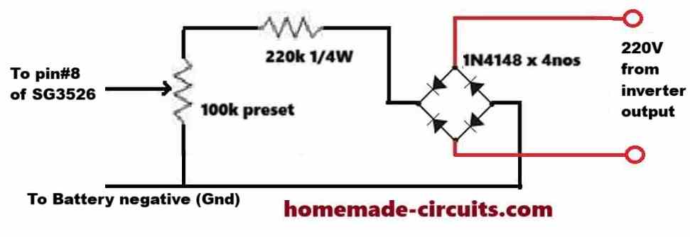
Hi swagatam
I really appreciate ☺️🙏🏾 your good work in creating time to tutor the people who are willing to learn circuit design’s. I really want to ask if they are ways we can have a pure sine wave H-bridge inverter circuit using dual PWM outputs IC’s such as SG3524,SG3525,TL494 and etc? That would be a great idea and advance design.
I will be waiting to hear from you 😊.
Thank you Emmanuel,
To convert a square wave H-bridge into a pure sine wave inverter you will have to inject a synchronized SPWM on the low side MOSFET gates.
You can combine the ideas presented in the following two articles for implementing the concept:
https://www.homemade-circuits.com/sg3525-pure-sinewave-inverter-circuit/
https://www.homemade-circuits.com/sg3525-full-bridge-inverter-circuit/
Possibly I will try to create a special article on this soon.
Hi swagatam
Can SPWM signal be fed in both high side MOSFET’S gate and low side MOSFET’S gate in a H-bridge inverter? Because I have seen some Indian made inverters with this type of configuration.
Hi Emmanuel,
Feeding the SPWM to high side mosfets in an N-channel MOSFET H-bridge setup may not be possible and is simply not required.
Because if you just control the low side MOSFETs with the SPWM, the output will automatically replicate the SPWM waveform correctly.
Good morning sir, Thanks for your effort in creating this site it’s really helping me, am following your circuit designs in my leaning. Please sir, I Made a transformer using the ic UC3845, 10k resistor an 202 capacitor for the timing which is about 36 kHz and my calculation was 12*10^8/4*36000frequency 1800Bmax*1.884area so I finally made it 3 tons as primary coil and I tested it with my 12 volts battery but my MOSFET is heating up PLEASE SIR I WANT TO KNOW WHETHER MY CALCULATION IS WRONG
Thank you Samson,
Really sorry, checking calculations can be extremely time consuming so that won’t be possible for me. Moreover, even i can make mistakes while calculating so my suggestions may not be confirmed.
I can help only with circuit diagrams within my range of expertise.
I like this. Can you help me do a modification of this for 70hz or 80hz? Also the output transformer needs to be a 1:1 or maybe a slight boost.
This should be 8.4 to 14.5 vac output at 70hz or 80hz (switched) with a max requirement of 300w continuous.
The frequency can be easily altered by adjusting the relevant RC timing components of the ICs.
The transformer can be also custom built but the number of turns will need to be correctly matched and optimized with the frequency, otherwise the MOSFETs might heat up.
To build the above designs an oscilloscope will be strictly required to verify the waveforms across the various stages.
Yep, I got an O scope on the way. I know it has to be dialed in just right. Thanks for the reply. Looking forward to getting started on this.
No problem Steve, all the best to you!
Hello, great topic. thank you.
may i have a conversation with you about designing a specific circuit that will take 12vdc and output 8-14 vac at a variable frequency of 50hz to 100hz pure sinewave and 10 to 30 amp power handling?
Hi, Thanks, and Glad you liked the post!
Making a sine wave oscillator is not difficult and can be easily done using a Bubba oscillator. The output current can be handled through a high current emitter follower transistor…however raising the 12V to 14V looks difficult and I am not sure how to do that in an easy way??
On the output transformer we can build a custom wound with the primary to secondary ratio of 1:1.2 or 10:12. But there should probably be a nice voltage regulator in an earlier stage. The more critical aspect I thing is the frequency as the motor is linear and optimized for specific frequency.. be it 70hz or 80hz depending on which one is used
My friend!
A ratio of 10:12 will give a high resistance to the windings and consequently limit the current through them, which will not allow the transformer to deliver the required power to the load.
Use the proper size, that’s how transformers are built. Please don’t attempt this if you haven’t the skills to so so.
The number of windings will have an effect on the voltage not the amperage rhe winding ratio is 1:10 for a 10x boost.
Again, please do not try this if you do not have adequate knowledge of what you are doing
Look, I’m not going to argue with you. I’m here for one reason and it’s not that. I know you are trying to help but I suggest you study up on transformers and how they function. Until then please refrain from continuing to respond to me. For research you might start with isolation transformers and buck/boost transformers.. but like I said, this post is not about transformers. So let’s please get back on track.
Thank you
Also, I forgot to mention before that this need not be synchronous to anything. It is a completely dedicated and separately derived output where the other components in this system will be DC. But with that for context. I will likely need some effective shielding from the rest of the electronics due to the strange frequency
The shielding can be perhaps done by using zener diodes and capacitors across the rest of the electronics to neutralize the frequency spikes and oscillations generated by the motor.
Interesting. Like on a ZVS flyback? I’m an electrician with only basic understanding of circuit design so this is a nice learning curve for me.
sir.. I can still use it for another project
thanks alot
good morning sir ????????????????
I will like to make this inverter but, I don’t know if the transformer can work bcs is not 12 0 12 transformer
is there anyway I can send you the picture just for you to see it
Hi Klin,
For the above SPWM sine wave inverter circuit with a 12V battery, a 12-0-12v transformer will not work….you will need a 6-0-6V transformer.
sir…. let’s consider Auto transformer for the project
OK, you can use an auto transformer.
thank you sir
how can I make a feedback circuit
like my power bank it turns on when the USB is plugged and turn off within short time
did you have any project related to that ??
????????
For feedback control you can try the second circuit from the following article:
https://www.homemade-circuits.com/load-independentoutput-corrected/
But this can be added later on, once you finish building the inverter circuit first.