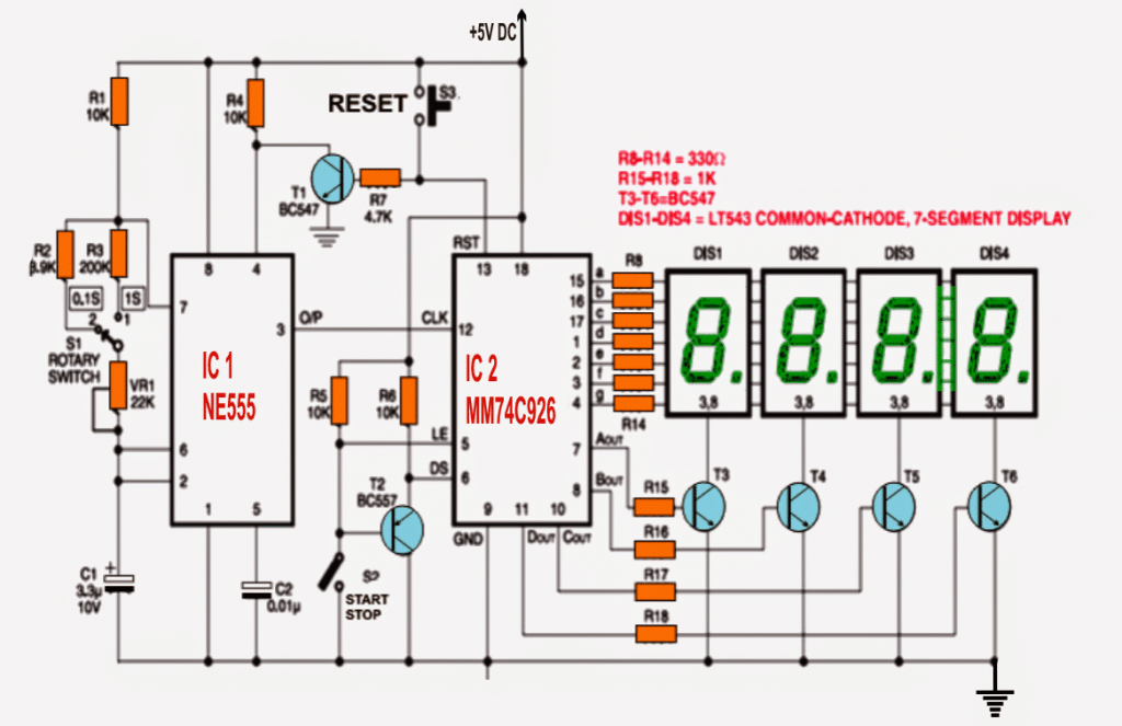
In this article we'll study a digital stopwatch design configured around the very popular IC LM555 in conjunction with a 4-digit counter IC with multiplexed 7-segment output drivers (MM74C926).
Written and Submitted by: Jennifer Goldy
Circuit Operation
IC MM74C926 is internally made up of a 4-digit counter, an output latch up stage, a npn output responsible for sourcing driver networks for common-cathode, 7-segment display and an internal multiplexing circuitry with four multiplexing outputs.
The multiplexing circuit stage also includes an in-built free running oscillator, and does not rely on any additional external frequency generating network.
The counter is designed to proceed on a negative rising of the clock signals.
The clock signal is manufactured by the timer IC LM555 (IC1) and impressed over pin 12 of IC2.A higher signal on reset pin 13 of IC2 resets the IC to zero logic.
Reset pin 13 is associated with +5V by means of a reset push-on-switch S3.
The moment S2 is is pressed even for a fraction of a second, the count figure is rendered to a zero logic, transistor T1 responds with a trigger and it resets IC1.
This enforces the counting to start in a situation wherein S2 is in ‘off’ condition.
Circuit Diagram

A low logic signal on the latch-enable input pin 5 (LE) of IC2 latches the count in the counter module into the on chip set output latches.
In an event when switch S2 is switched ON, pin 5 is forced to go low and thereby the count figure is allowed to be saved in the latch section of the IC.
Display-select pin 6 (DS) ascertains if the figure on the counter or the stored count in the latch may be shown on the display or not.
In case pin 6 is held low the figure in the output latch section is enabled to get displayed, however if pin 6 is rendered with a high logic the count stored in the counter is illuminated over the connected display.
On an occasion when switch S2 is switched, the base of pnp transistor T2 is linked with ground ensuring that it begins operating. The emitter of T2 is rigged with DS pin of IC2.
Consequently, whenever switch S3 is switched ON, reset pin 13 of IC2 is coupled with negative through the transistor T1 making sure that the oscillator is inhibited from generating clock pulses. This operation is executed to implement a synchronization between IC1 and IC2.
At the first level, reset the module in order to enable the display to show ‘0000.’ Next disconnect switch S2 for the stop watch to initiate its counting the periods. In case you wished to inhibit the clocking of the chip, simply switch OFF the control S2.
The given rotary switch S1 may be opted for selecting the many different time intervals at the output of the astable multivibrator (IC1).
The proposed digital stopwatch circuit will work off a 5V supply inputs. The circuit may be easily fixed and built on a general-purpose PCB.
You may want to enclose the entire circuit in a metallic cabinet with slots built for four 7-segment displays, rotary switch S1, start/stop switch S2 and reset switch S3 in the dashboard plate of the selected encloser.
Main Specifications of the IC MM74C926:
- Supply Voltage (Vdd): 3V to 15V
- Logic Type: CMOS
- Current Consumption: Low power due to CMOS technology
- Clock Frequency: Up to 3 MHz at 10V
- Output Type: Common cathode 7-segment LED display driver
- Digits Supported: 4 digits (multiplexed)
- Package Type: DIP or SOIC
- Operating Temperature Range: -40°C to +85°C
Pin Configuration:
- Clock (CLK): Input for incrementing the counter.
- Reset (RST): Input to reset the counter to zero.
- Latch Enable (LE): Controls data latching for display updates.
- Display Outputs: Segment outputs (a, b, c, d, e, f, g) for driving a common cathode 7-segment display.
- Digit Select Outputs (D1-D4): Used for multiplexing the 4 digits.
Related Formulas:
Frequency of Oscillation (Internal Clock) can be calculated using the following formula:
f = 1 / (Rt * Ct)
- Rt: Resistor connected to the clock pin
- Ct: Capacitor connected to the clock pin
Current through Segment LEDs can be calculated using the following formula:
- Iseg = (Vdd - Vseg) / Rseg
- Vseg: Forward voltage drop of the LED segment (typically 2V for red LEDs)
- Rseg: Series resistor value for limiting current
Maximum Display Frequency (Multiplexing) can be calculated using the following formula:
- fdisp = fclk / 4
- fdisp: Effective refresh rate for each digit
- fclk: Input clock frequency
