

A digital-to-analog converter (DAC, D/A, D2A, or D-to-A) is a circuit designed to convert a digital input signal into an analog output signal. The analog-to-digital converter (ADC) works in the opposite way and transforms an analog input signal into a digital output.
In this article I will comprehensively discuss how digital to analog, and analog to digital converter circuits work, using diagrams and formulas.

In electronics we may find voltages and currents varying continuously with different ranges and magnitudes.
In digital circuits the voltage signal is in two forms, either as a logic high or logic low logic levels, which represent binary values of 1 or 0.
In a analog to digital converters (ADC), the input analog signal is represented as a digital magnitude, while a digital-analog converter (DAC) converts the digital magnitude back to an analog signal.
How Digital-to-Analog Converters Work
Digital-to-analog conversion process can be carried out through many different techniques.
One well-known method utilizes a network of resistors, known as ladder network.
A ladder network is designed to accept inputs involving binary values typically at 0 V or Vref and delivers an output voltage equivalent to the magnitude of the binary input.
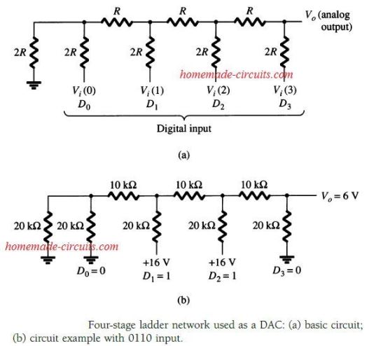
The figure below demonstrates a ladder network using 4 input voltages, that represent 4 bits of digital data and a dc voltage output.
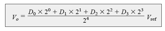
The output voltage is proportionate to the digital input value as expressed by the equation:


Solving the above example we get the following output voltage:

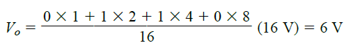
As we see, a digital input of 01102 gets converted to an analog output of 6 V.
The purpose of the ladder network is to change the 16 potential binary magnitudes
through 0000 to 1111 into one of the 16 voltage quantities at intervals of Vref/16.
Therefore, it may be possible to process more binary inputs by including more number of ladder units, and to accomplish higher quantization for each step.
Meaning, suppose if we use a 10 step ladder network, will allow use to increase the voltage step quantity or the resolution to Vref/210 or Vref/1024. In this case, if we used a reference voltage Vref = 10 V would generate output voltage in steps of 10 V / 1024, or at around 10 mV.
Thus, adding more number of ladder stages will give us proportionately higher resolution.
Typically, for n number of ladder steps, this can be represented through the following formula:
Vref / 2n
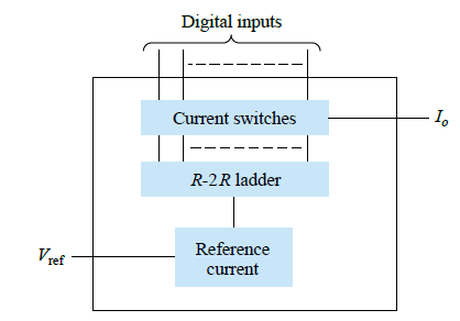
DAC Block Diagram
The figure below shows the block diagram of a standard DAC using a ladder network, referenced as a R-2R ladder. This can be seen locked between reference current source and current switches.
The current switches are linked with the binary switches, producing an output current proportional to the input binary value.
The binary inputs toggle the respective legs of the ladder, enabling an output current that's a weighted sum of the current reference.
If required, resistors can be attached with the outputs for interpreting the result as analog output.

How Analog-to-Digital Converters Work
So far I have explained how to convert digital to analog signals, now I have explained how to do the opposite, that is convert an analog signal into a digital signal. This can be implemented through a well known method called the dual-slope method.
The following figure shows the block diagram for the standard dual slope ADC converter.

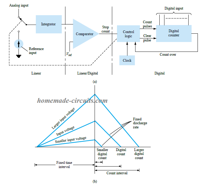
Here, an electronic switch is employed to transfer the desired analog input signal to an integrator, also called a ramp generator. This ramp generator may be in the form of a capacitor charged with a constant current for generating the linear ramp. This produces the required digital conversion through a counter stage that works for both positive and negative slope intervals of the integrator.
The method may be understood with the following description:
The full measuring range of the counter decides the fixed time interval. For this interval the input analog voltage applied to the integrator causes the comparator input voltage to rise to some positive level.
Referring to the (b) section of the diagram above, shows that the voltage from the integrator at the end of the fixed time interval is higher than the input voltage that's larger in magnitude.
When the fixed time interval finishes, the count is set to 0, which prompts the electronic switch to connect the integrator to a fixed reference input voltage level. After this, the output of the integrator which is also the input of the capacitor begins dropping at a constant rate.
During this period, the counter keeps advancing, while the output of the integrator continues to drop at a constant rate, until it goes below the reference voltage of the comparator. This causes the comparator output to change state and triggers the control logic stage to stop the counting.
The stored digital magnitude inside the counter becomes the digital output of the converter.
The use of a common clock and integrator stage during both the positive and negative slope intervals adds some sort of compensation for controlling the drifting of the clock frequency, and accuracy limit of the integrator.
It may be possible to scale the counter output as per user preference by suitably setting up the reference input value, and the clock rate. We can have the counter as binary, BCD or in other digital format, if it's required.
Using Ladder Network
The ladder network method using counter and comparator stages is another ideal way to implement analog-to-digital conversion. In this method, a counter begins counting from zero, which drives a ladder network, generating a stepped incrementing voltage, resembling a staircase (see figure below).

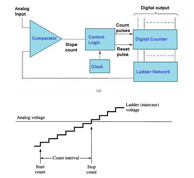
The process allows the voltage to increase with each count step.
A comparator monitors this incrementing staircase voltage and compares it with the analog input voltage. As soon as the comparator senses the staircase voltage going above the analog input, its output prompts to stop the counting.
The counter value at this point becomes the digital equivalent of the analog signal.
The level of change in the voltage generated by the steps of the staircase signal is determined by the amount of count bits used.
For example a 12 stage counter using 10 V reference will operate a 10 stage ladder network with step voltages of:
Vref/212 = 10 V / 4096 = 2.4 mV
This will create a conversion resolution of 2.4 mV. The time required for the execution of the conversion is determined by the clock rate of the counter.
If the clock rate of 1 MHz is used for operating a 12 stage counter, the maximum time taken for the conversion would be:
4096 x 1 μs = 4096 μs ≈ 4.1 ms
The least number of conversions that may be possible per second can be found as:
no. of conversions = 1/4.1 ms ≈ 244 conversions/second
Factors that Influence the Conversion Process
Considering that some conversion may demand higher and some may require lower count time, typically a conversion time = 4.1ms / 2 = 2.05 ms can be a good value.
This will produce a 2 x 244 = 488 number of conversions on an average.
Slower clock rate would mean less conversions per second.
A converter working with lower number of count stages (low resolution) would have a higher rate of conversion.
The precision of the of converter is determined by the accuracy of the compartaor.