In electronics, rectification is a process in which a rectifier diode converts an alternating full cycle AC input signal into a half cycle DC output signal.
A single diode produces half wave rectification, and a network of 4 diodes produces a full wave rectification
In this post we will analyze both half wave and full wave diode rectification processes, and other properties through time-varying functions like sine wave and square wave. Meaning, through voltages and currents which change their magnitude and polarity with respect to time.
We will consider the diode to be an ideal diode by ignoring whether it's a silicon diode or a Germanium, to minimize complications in the calculations. We will consider the diode to be a standard rectifier diode with standard rectification abilities.
Half-Wave Rectification
The simplest diagram showing a time-varying signal applied to a diode is shown in the following diagram:
Here we can see an AC waveform, where the period T signifies one full cycle of the waveform, which is the average value or the algebraic sum of the portions or the humps above and below the central axis.

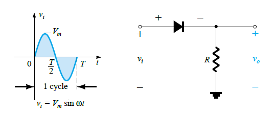
This type of circuit in which a single rectifier diode is applied with a time-varying sinusoidal AC signal input to generate a DC output having a value half of the input is called a half wave rectifier. The diode is referred to as the rectifier in this circuit.
During the period between t = 0 → T/2 of the AC waveform, the polarity of the voltage vi creates a "pressure" in the direction as depicted in the diagram below. This allows the diode to switch ON and conduct with a polarity as indicated just above the diode symbol.

Since the diode is conducting fully, substituting the diode with a short circuit, will produce an output as shown in the above right side image.
No doubt, the generated output appears to be an exact replication of the applied input signal above the central axis of the waveform.
During the period T/2 → T, the polarity of the input signal vi becomes negative, which causes the diode to turn OFF, resulting in an open circuit equivalent across the diode terminals. Due to this the charge is unable to flow across the diode path during the period T/2 → T, causing vo to be:
vo = iR = 0R = 0 V (using Ohm's Law). The response can be visualized in the following diagram:

In this diagram we can see the DC output Vo from the diode produces a net average positive region above the axis, for the input full cycle, which can be determined by the formula:
Vdc = 0.318 Vm (half-wave)
The input vi and the output vo voltages during the diode half-wave rectification process is presented in the following figure:
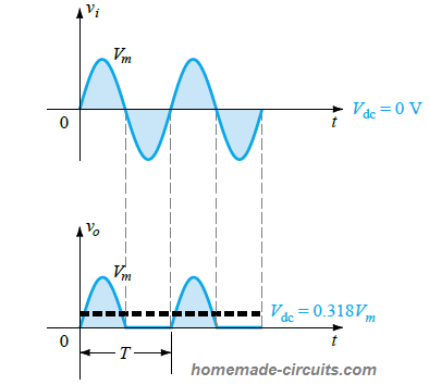
From the above diagrams and explanation we can define half-wave rectification as a process in which one-half of the input cycle is eliminated by the diode at its output.
Using a Silicon Diode
When a silicon diode is used as the rectifier diode, since it has a forward voltage drop characteristic of VT = 0.7 V, it generates a forward bias region as shown in the following figure:

The VT = 0.7 V means that now the input signal must be at least 0.7 V to ensure the diode turns ON successfully. In case the input VT is less than 0.7 V would simply fail to switch ON the diode and the diode will continue to be in its open circuit mode, with Vo = 0 V.
While the diode conducts during the rectification process, it generates a DC output that carries a fixed voltage level for the voltage difference vo - vi, equal to the above discussed forward drop of 0.7 V. We can express this fixed level with the following formula:
vo = vi - VT
This produces a reduction in the average output voltage above the axis, causing a slight net reduction of the rectified output from the diode.
Referring the above figure, if we consider the Vm (peak signal level) to be adequately high than the VT, such that Vm >> VT, we can evaluate the average DC output value from the diode using the following formula, quite accurately.
Vdc ≅ 0.318(Vm - VT)
More precisely, if the input AC peak is sufficiently higher than VT (forward drop) of the diode, then we can simply use the previous formula for estimating the rectified DC output from the diode:
Vdc = 0.318 Vm
Solved Example for Half Bridge Rectifier
Problem:
Evaluate the output vo and find out the DC magnitude of the output for the circuit design shown below:
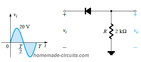
Solution: For the above circuit network, the diode will turn ON for the negative portion of the input signal, and vo will be as indicated in the following sketch.

For the full period of the input AC cycle, the DC output will be:
Vdc = 0.318Vm = - 0.318(20 V) = - 6.36 V
The negative sign indicates the polarity of the output DC which is opposite to the sign provided in the diagram under the problem.
Problem#2: Solve the above problem considering the diode to be a silicon diode.
In case of a silicon diode, the output waveform would look like this:
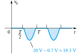
And the output DC would can be calculated as I have explained below:
Vdc ≅ - 0.318(Vm - 0.7 V) = - 0.318(19.3 V) ≅ - 6.14 V
The drop in the output DC voltage due to the 0.7 V factor is around 0.22V or approximately 3.5%
Full-Wave Rectification
When an AC sinusoidal signal is used as the input for rectification, the DC output can be improved to 100% level using a full-wave rectification process.
The most well known and easy process for achieving this is by employing a 4-diode bridge rectifier network as shown below.
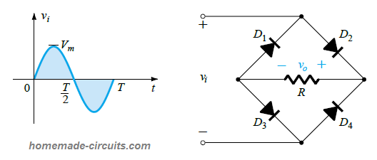
When the positive input cycle progresses through the period t = 0 to T/2, the polarity of the input AC signal across the diode and the output from the diode are as represented below:
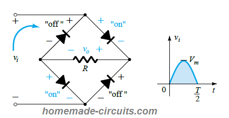
Here, we can see that due to the special arrangement of the diode network in the bridge, when D2, D3 conduct, the opposite diodes D1, D4 remain reversed biased and in switched OFF state.
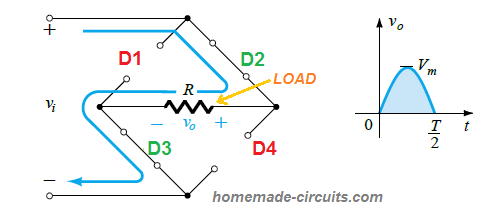
The net output DC generated from this rectification process through D2, D3 can be seen in the above diagram. Since we have imagined the diodes to be ideal, the output is vo = vin.
Now, likewise for the negative half cycle of the input signal diodes D1, D4 conduct, and diodes D2, D3 go into an OFF state, as illustrated below:

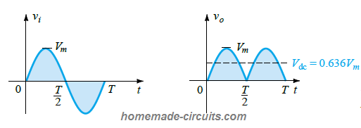
We can clearly see that the output from the bridge rectifier has converted both the positive and the negative half cycles of the input AC into two DC half cycles above the central axis.
Since this region above the axis is now two times more than the region obtained for a half wave rectification, the output DC will also become twice the magnitude, as calculated using the following formula:
Vdc = 2(0.318Vm)
or
Vdc = 0.636Vm (full-wave)
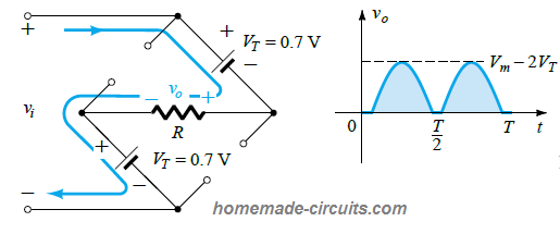
As depicted in the above figure, if instead of ideal diode a silicon diode is used, applying Kirchhoff’s voltage law over the conduction line would give us the following result:
vi - VT - vo - VT = 0, and vo = vi - 2VT,
Therefore, the output voltage peak vo will be:
Vomax = Vm - 2VT
In a situation where V >> 2VT, we can use our earlier equation to get the average value with a reasonably high degree of precision:
Vdc ≅ - 0.636(Vm - 2VT),
Yet again, if we have Vm significantly higher than 2VT, the 2VT can be simply ignored, and the equation can be solved as:
Vdc ≅ - 0.636(Vm)
PIV (Peak Inverse Voltage)
The peak inverse voltage or the (PIV) rating which is also sometimes called peak reverse voltage (PRV) rating of a diode becomes a crucial parameter while designing rectifier circuits.
It is basically a reverse-bias voltage range of the diode that must not be exceeded, otherwise the diode may breakdown by transiting into a region called zener avalanche region.
If we apply Kirchhoff's voltage law to a half wave rectifier circuit as shown below, it simply explains that the PIV rating of a diode must be higher than the peak value of the supply input used for the rectifier input.
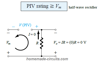
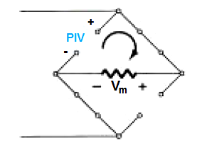
For a full bridge rectifier also, the PIV rating calculation is the same as half wave rectifier, that is:
PIV ≥ Vm, since Vm is the total voltage that's applied to the connected load as depicted in the following figure.
Solved Examples for Full Bridge Rectifier Network
Determine the output waveform for the following diode network, and also calculate the output DC level and the safe PIV for each diode in the network.
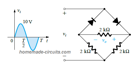
Solution: For the positive half cycle, the circuit would behave as depicted in the following diagram:
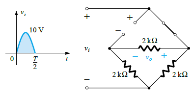
We can redraw this in the following manner for better understanding:
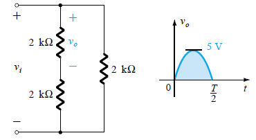
Here, vo = 1/2vi = 1/2Vi(max) = 1/2(10 V) = 5 V
For the negative half cycle, the conduction role of the diodes can be interchanged, which will produce an output vo as shown below:
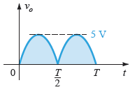
The absence of two diodes in the bridge results in the reduction in the DC output with a magnitude:
Vdc = 0.636(5 V) = 3.18 V
This is quite the same that we would have obtained from a half bridge rectifier with the same input.
The PIV will be equal to the maximum voltage generated across R, which is 5 V, or half of that needed for a half wave rectified with the same input.
Dear Swagatham
The forward voltage drop (VF) of a silicon diode is 0.7v. This is what I understand from many circuit discrptions.
But the datasheet of 1N4007 says the Vf is 1.1V. Why this difference…..?
Thanks in advance.
Dear Anil, 1.1V could be the maximum possible specification of the diode, but usually it is below 0.7V…you can practically confirm this through a DMM set at the diode range.