Contact mics can be used to sense unusual sounds when attached to various surfaces.It also Produce sound when voltage is applied to it.With the help of a basic Pre-amp circuit it can also be used to Electrify an Acoustic Guitar, where amplification is a must.
Written and Submitted by: Ajay Dusa
Piezoelectric Disc as the Sensor
A piezoelectric disk generates a voltage when deformed. Piezo elements come in handy when you need to detect vibration or a knock. You can use these for tap or knock sensors pretty easily by reading the voltage on the output. They can also be used for a very small audio transducer such as a Buzzer.
The trick is the preamp – a basic circuit used to match the piezo’s signal.
The resulting piezo/preamp combo can be used for electrifying an acoustic guitar.
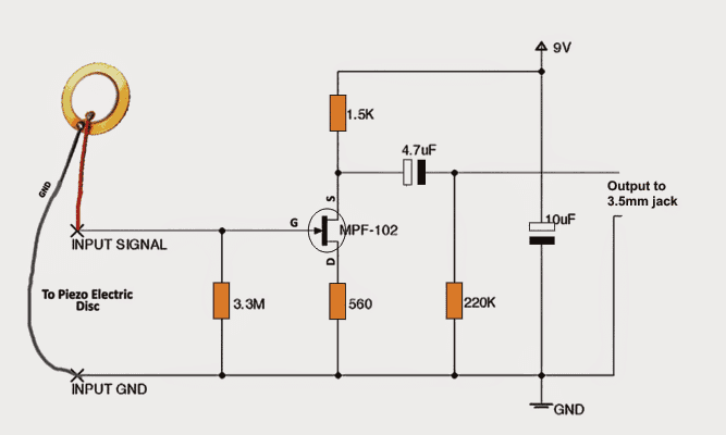
Circuit Diagram

Circuit Operation
The battery supplies +9 volts which is connected to the source of the JFET device, MPF-102. This voltage is connected to the source through source resistor 1.5K.
One terminal of this amplifier is common to both the input and output signals. This terminal is the JFET drain terminal.
For this reason, we sometimes call this amplifier circuit a "common drain circuit”.The Drain resistor 220k is connected to the source to the battery's ground terminal.
Using MPF-120
The main Element used in the circuit is the MPF-102 Transistor.
Under no-signal conditions, bias voltage causes the JFET source to draw a very small current. This current sets the source voltage at a point halfway between the Supply and ground.
This is the recommended bias setting for most small-signal or analog audio amplifiers.It allows the maximum signal before distortion.
The signal enters the amplifier through gate resistor 3.3M. The voltage drop across 3.3M is the input signal at the JFET gate. This signal is an AC voltage.
How JFET Works
The signal enters JFET,which is a amplifying device.The difference between the source and the gate sets the voltage drop across resistor 560 Ω.
Normally, the bias voltage across resistor 560 Ω holds the JFET channel at a medium resistance value. The bias voltage is a DC voltage. When we apply a signal, the input signal varies the negative bias voltage across resistor 560 Ω.
The varying gate signal causes the JFET's to vary. For this reason, more or less current passes through the JFET.
The source resistor 1.5K converts the current variations to voltage variations. Since the input signal controls the channel width.That is, a small signal controls a large signal. In our case, the JFET gate voltage controls the JFET source current. This result’s in Amplification.
The output signal appears between the Source and ground. Capacitor 4.7uF blocks the DC voltages in the circuit, but passes the amplified AC signal.
The gate is more negative than the ground terminal. Now the output comes out across the Source and ground. But we've connected the Source to Supply.
Then the Source is more positive than the ground terminal. With the gate negative and the Source positive, This output signal exits the amplifier through capacitor 4.7uF and appears across resistor 220k. This Capacitor blocks DC and passes only.
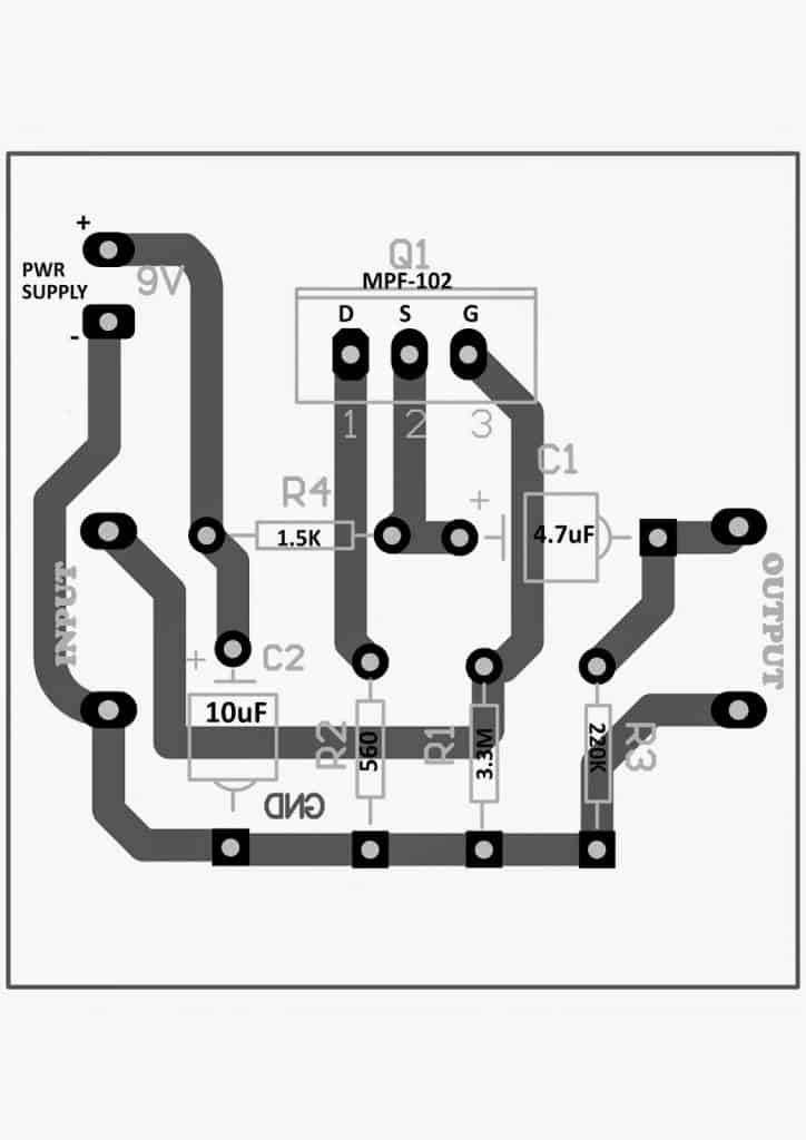
PCB Design for the above explained DIY contact MIC circuit

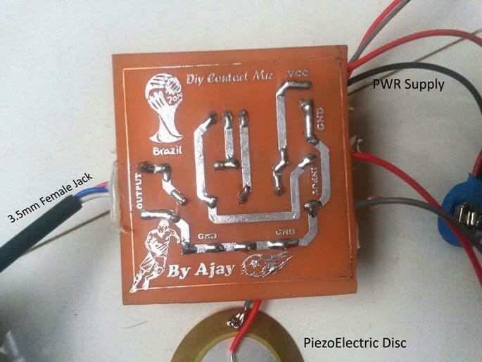
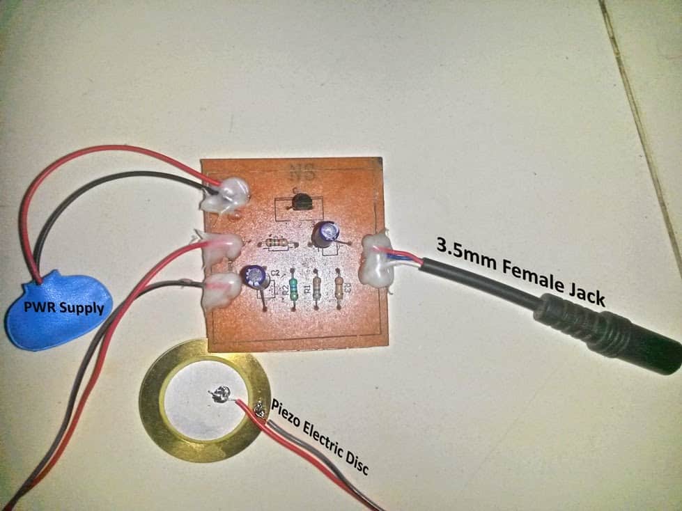
Following are the images of the DIY contact mic prototype, built and submitted by Mr.Ajay Dusa


