In the following post I have explained two straightforward dummy load circuits: the first one can be used for testing high current power supplies, and the second design can be used for testing large power amplifiers.
Suppose you have a 10 amp power supply and you want to confirm the 10 amp output through some sort of dummy load which can absorb 10 amp current. For this, you would have to build a 10 amp current sink using many high watt resistors connected in series and parallel. This arrangement could be hugely cumbersome and bulky.
Instead, an adjustable transistorized dummy load circuit could do the job more efficiently by sinking the 10 amp current from the power supply and help the user to confirm that the power supply is actually able to deliver the intended 10 amp current.
In this circuit, the high power transistors could be optimized and adjusted to sink or shunt the power supply current at some specific rate, which could be adjusted through a potentiometer, thus making the procedure very smooth and accurate.
You can test power supplies and related devices at maximum peak output current without resorting to arrays of power resistors, using this dummy load circuit, which is nothing but a simple transistor current sink circuit.
Without the need of costly non-inductive resistors, an adjustable current sink permits the load to be adjusted fast across a large range, irrespective of the voltage source. And thus removes the need to fiddle with power resistors each time the voltage and/or output current characteristics of the power supplies or devices under test are changed, for example during the testing of power supplies.
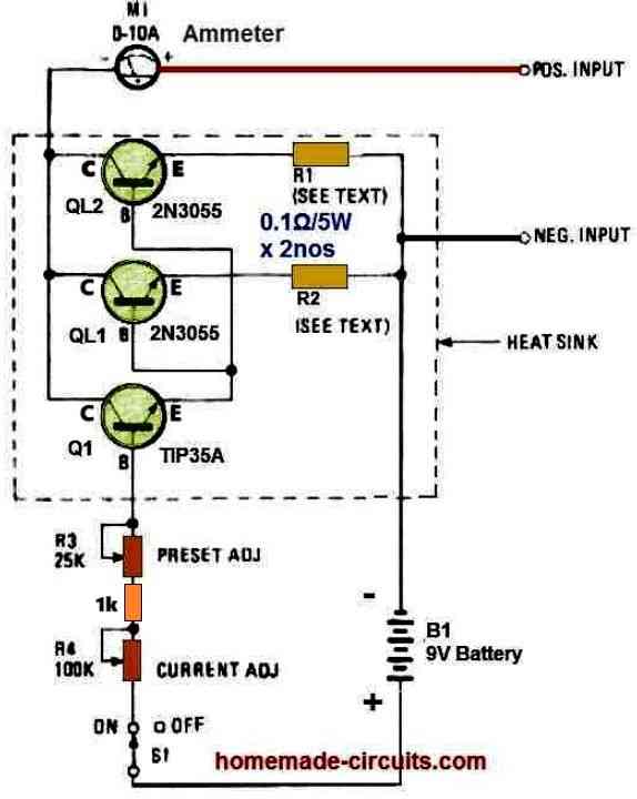
How the Circuit Works
The current load is shared by transistors QL1 and QL2, which are balanced by their emitter resistors R1 and R2, whose quantities should be in the.2 ohm to.1 ohm range.
Therefore, simply by connecting power transistors QL1 and QL2, we may raise the circuit's current-load capacity to whatever we want, restricted by just the transistors' absolute limits.
A few common junkbox-type load transistors, like for example NPN 2N3055s, may come with a VCE of 60 volts, an Ic at about 15 amps, and power dissipation of 115 watts.

Thus, everything else being identical, while assessing low-voltage supplies, power dissipation is the most important characteristic to consider.
For instance, you may be able to handle 30 volts at 20 amps constantly by connecting four ordinary junkbox 2N5885s in parallel with four 0.1 ohm, 5 watt emitter resistors. 2N5885s have similar characteristics to 2N3055s, although with a power dissipation in the 200-watt range, and with a collector current Ic of about 25 amperes.
Furthermore, high-voltage power supply could also be tested if transistors having high VCE specifications are incorporated.
In either circumstances, the bases of the load transistors (QL1 and QL2) are governed by a predetermined "adjust" current through a battery or DC power. This preset current regulates the current flowing via Q1, that controls the base current of load transistors QL1 and QL2.
PRESET ADJ., potentiometer R3, controls the highest allowable current draw, whereas CURRENT ADJ., potentiometer R4, sets the current range.
Transistor Q1 is a typical TIP35A, an NPN silicon power transistor that may withstand voltages up to 350 and also has a rated collector current of one amp.
In this dummy load circuit, any NPN silicon power transistors featuring a hfe of 50-150 would suffice. 2N5682 is yet another possibility for Q1.
How to Setup
The setting level of the PRESET potentiometer, R3, is defined by the beta of the transistors employed, and the higher-load threshold is decided by the load transistors.
The maximum load is adjusted by potentiometer R3, and the current level is readily adjusted if an optional ammeter or external ammeter is installed. To begin with, tweak the current PRESET potentiometer R3 to maximum and the CURRENT ADJ. potentiometer R4 to the lowest resistance.
Next, measure the current consumed from an appropriate power source hooked up to this active dummy load and adjust the current-preset to achieve the maximum load you intend to implement; and that's all there is to it!
The maximum power dissipation required is determined by the number and kind of load transistors employed.
Therefore, if you drive a lot of voltage at an excessive current for an extended length of time, don't exceed their maximum power dissipation otherwise you might fry your load transistors.
Alternatively , if you allow your load transistor temperature to normalize for a short amount of time, it might perhaps allow you to exceed their continuous power dissipation limit.
Try implementing a moderate duty cycle which does not go beyond their optimal working temperature.
This project does not provide a components list since doing so would undermine the objective of the project, which is to be made from junk box parts. A 9-volt transistor battery was selected since it works like an optimum control power source which is electrically isolated-while lowering expenses to a bare minimum.
Calculations and Formulas
In the circuit the TIP35A transistor (Q1) combined with the two 2N3055 transistors (QL1 and QL2) forms a Darlington configuration which greatly increases the current gain, as the overall current gain of a Darlington pair is approximately the product of the individual current gains of the two transistors.
Darlington Configuration in the Circuit:
TIP35A (Q1) acts as the driver transistor.
2N3055 transistors (QL1 and QL2) serve as the power-handling transistors,, sharing the load current.
Current Gain in Darlington Configuration:
The effective current gain (h_FE(total)) of the Darlington pair can be approximated as:
hFE(total) ≈ hFE(Q1) × hFE(QL1)
Where:
hFE(Q1) is the current gain of the TIP35A (typically it is around 20 at high currents).
hFE(QL1 or QL2) is the current gain of the 2N3055 (typically this is around 20 at high currents).
So the overall current gain becomes:
hFE(total) ≈ 20 × 20 = 400
This means that only a small base current is required to drive the Darlington configuration to handle large load currents.
Base Current Calculation for TIP35A (Q1):
Since the Darlington pair has a very high current gain, the base current required for Q1 is:
IB(Q1) = ILoad / hFE(total)
For a maximum load current of ILoad = 10A:
IB(Q1) = 10A / 400 = 0.025A (25mA)
This is significantly smaller compared to the base current required for individual 2N3055 transistors without the Darlington configuration.
Resistor Calculations:
R3 (base resistor for Q1):
The voltage across R3 remains VR3 = 9V - VBE(Darlington).
In a Darlington configuration the base-emitter voltage is approximately:
VBE(Darlington) = VBE(Q1) + VBE(QL1)
Typically each of the base-emitter junctions has a voltage drop of around 0.7V therefore:
VBE(Darlington) ≈ 0.7V + 0.7V = 1.4V
The voltage across R3 is:
VR3 = 9V - 1.4V = 7.6V
To allow IB(Q1) = 25mA:
R3 = VR3 / IB(Q1) = 7.6V / 0.025A = 304Ω
You can choose a standard resistor value: R3 ≈ 300Ω.
Power Dissipation in the Transistors:
In a Darlington configuration the TIP35A (Q1) specifically handles the small base current for the 2N3055 transistors and thus its power dissipation is much lower.
The 2N3055 transistors share the majority of the load current (5A each for a 10A load).
For each 2N3055:
PQL = VCE × IC
Assuming VCE = 5V and IC = 5A:
PQL = 5 × 5 = 25W
Both the 2N3055 transistors need to dissipate 25W each which means appropriate heat sinks are critical.
Finalized Component Values for Optimal Dummy Load Operation
- R1, R2: 0.1Ω, 5W (to balance current sharing between the 2N3055 transistors).
- R3: 300Ω, 1W (limits the base current for the TIP35A).
- TIP35A (Q1): Acts as the driver in the Darlington pair.
- 2N3055 (QL1, QL2): Handle the main load current, requiring good heat sinks.
- Power Source: A 9V battery powers the base circuit.
- Load Current: Up to 10A, shared equally by the two 2N3055 transistors.
- This ensures that the Darlington configuration works efficiently to drive the high current load using minimal base current.
Dummy Load for Testing Power Amplifiers
The following dummy load circuit can be effectively used for testing large power amplifiers with 8 ohm speaker specifications.
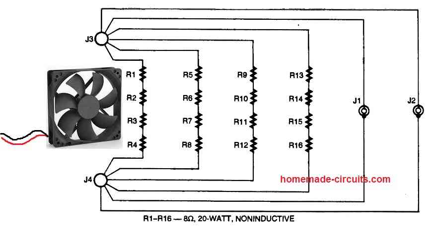
The circuit is quite easy to build, but after building it, and before testing make sure to check the following conditions carefully:
Check the fan, make sure it spins correctly and produces optimal breeze, when switched ON.
Using an OHM meter check across J1, J2, you must see 8 ohms on the meter. Do the same across J3, J4, and the result should be the same, that is 8 ohm reading on the meter.
To test a power amplifier with this dummy load, you must connect the amplifier output across J1, and J2. Preferably, connect the ground side of the amplifier output with J2.
Connect a distortion analyzer meter across J3, J4.
Connect a 1 kHz oscillator frequency to the input of the amplifier.
Switch ON the fan, and then switch ON the amplifier and the 1 kHz oscillator.
After this you can check the amplifier distortion response on the distortion analyzer meter.
Make sure to use a cooling fan which effectively keeps the dummy load resistors cool for at least 5 minutes.
Testing the dummy load over 5 minutes is not recommend, otherwise it may cause damage to the resistors.
Remember to use resistor which are not wire-wound type, because wire-wound resistors can become inductive and produce wrong results on the distortion analyzer meter, and may cause the resistors to over heat.
Hi Swagatam;
My dummy load max. current would be 2A. And in this sample I use 220AC to 12V DC 2A adapter / power supply as the load. So as per your below confirmation I used single TIP3055 and a TR 22N2222. In case I use the low resistance value to the base of the 2N2222 then the TIP3055 is overheating. But if I use the higher value resistance to the base of the 2N222 then the multimeter displays the lower current rate on the screen. As a result I think the power supply may not be the proper load or I should add another TIP3055 to the circuit or I would measure the load in very short period to eliminate the overheating. Could I have your opinion on the matter please?
Hi Suat,
Since this circuit is supposed to work like a dummy load so the transistor will heat up, and you must add a large heatsink to it. Dummy loads are specifically designed to dissipate heat.
However at 2 amp the 2N3055 should never overheat, I think your 2N3055 may not be good.
Anyway a heatsink is a must for this application…
Hi Swagatam, I have used TIP3055 and 2N2222. And There are serial connected resistors 1K + 22K and the 100K pot between the 2N2222 base and 9V input for the test purposes. And I have 2 adapters with the specs.; 220 Input 12V DC Output 2A and 220 Input 12V DC output 1A. I test them respectively and 1A adapter shows about 1,2A on the multimeter and 2A adapter shows about 1,8A. And also the pot seems ineffective to adjust the current rate. Could you please share your comment?
Hi Suat,
Please replace the 2N2222 with TIP35, or 2N3055 and check again. 2N2222 has a high gain, that is why the 100k might not be limiting the current.
Or if you are using 2N2222 try 1M pot instead of 100k.
Also, 1 amp is very less current, the pot is supposed to work for currents over 5 amps.
I am sorry Swagatam, I have forgotten to mention that I used single TIP3055 since I will not measure higher than the 2A load. OK I will place 1M ohm as the base resistance.
Sure, no problem Suat, let me know how it goes…
Hi Mr. Swagatam;
Is it possible to use a small value resistor just like 1 or 10 ohm between the TIP35 collector and the 2N3055 base in order to protect the 2N3055 against any undesirable defect.
Hi Suat,
Do you mean a resistor between TIP35 Emitter and 2N3055 base?
Yes you can use it.
Thanks Swagatam but I think there is a small mistake at the above diagram since the arrow signs are marked as the emitter whereas it is written as the collector. Could you please check that one for me.
Thank you Suat, for pointing the typo error, I have corrected the error and updated the diagram accordingly, you can check it now…
Hi Mr. Swagatam;
I used one TIP3055 (instead of 2N3055) and a TIP31c(instead of TIP35A) and the load was my 12V 2A transformer. I saw about 1,3A on the display of the multimeter and the tip3055 was too hot. Is it normal or I made something wrong?
P.S.: I had not used heat sink due to low current at the circuit.
Hi Suat,
Your BJTs are correct.
1.3 amps is quite less for the two TIP3055 to become hot. It shouldn’t be.
There’s one small issue in the diagram. The two presets R3 and R4 must also have a 1k resistor in series, because if by mistake both the presets are adjusted to zero ohms, then the transistors might burn, so please add a 1k in series with the R3, R4.
Thanks Swagatam. I use a single TIP3055 because I will test max 2A load capacity. I have added 2K2 Ohm resistor in serial with the only 100K pot to the base of the TIP35. My test device is 12V DC 2A transformer. In the case what should the emitter voltage be while the test? Would it be the same with the transformer voltage as the 12V or I will see the current value from the ammeter as the voltage?
Hi Suat,
The emitter output voltage must be around 1.5V lower than the collector voltage of your 2N3055.
Also, if possible please try 2N2222 in place of the TIP35 for better current drive for the 2N3055 and and better conduction…
What size of heat sink would you need to comfortably run 400W through the circuit?
Thanks,
J
That will need to be tested practically, it is difficult to provide an estimated figure.
Hello, good afternoon, I like this circuit, but I would like to know how to make an electronic load to measure low charges… From 1ma to 2A.. Thank you very much
Hi, to check smaller currents, you can replace the transistors with 2N2222 and replace the emitter resistors with higher values resistors, and also replace the meter with a 2 amp meter.
Hi how are things. Thank you very much for the circuit and the explanation. I’ll be building this phantom charge as I regularly repair power sources. I wanted to point out that in the circuit the Emitter “E” and the Collector “C” are marked backwards. The “E” is on the Collector and the “C” is on the Emitter.
Greetings.
Oh yes!! that looks like a bad printing mistake. I hope the readers will understand the mistake and ignore it. Thanks very much for pointing it out.
Regarding my last post, May 16, 2022, I have drawn a full schematic of the dummy load. I have been looking all over for a conversion for the chip that controls it with no joy. Chip f 7-6699 below that 1418. Now the schematic is now a professional one but I don’t think there a many mistakes. I have been checking and checking as I go. Would mind looking at it and see if you can reverse engineer it. I can make a foto of the unit, I have it opened up, if you would like, and a copy of the schematic to your e-mail. Thanks, Bruce Kalashian
You can upload the schematic on any free image hosting site and provide me the link here, I will check it out.
I have a electronic dummy load with 4 to-3 transistors on heat sink driven with one 3055 with two huge caps a crossed them, and controlled by a 14 pin IC (f-7-6699 and under that 7419) and included with a huge transformer. Powered by 150 vac. and can handle up to 100 amps. I got it from a friend and mentor who was really very knowledgeable. He told me it was just a reverse power supply. Unfortunately he has died so I can’t find out what the IC is and the markings don’t come up on Google. It worked the other day and the next time I tried to use it, nothing. I have checked most all of the components, pots, diodes, caps and what not, it is very complicated and way out of my experience. I kinda think the IC died but I am not sure because I don’t know how the thing works.Any help would be appreciated. thanks. BK
I am sorry, it can be very difficult to judge the fault without checking the unit practically, because it can be the IC that has gone bad or it could be one of the transistors.
By the way your IC could be a 7419 IC which is a Hex Inverter Schmitt trigger IC, and it is easily available in the market.
Thanks for the very nice circuit and explanation. I recreated the circuit with stuff from my junk box but as I try to regulate it, Im getting into the following problem
as I higher the voltage to be tested, I reach a breakdown point (probably the Emmiter-Base breakdown voltage of 6V) where my potentiometer doesn’t have any effect on the circuit which draws a lot of current.
So if I get it correctly this circuit (supplied with 9V) can test loads of up to 9+6V=13V ???
And If I higher the base voltage to lets say 15V with a step up converter, I can test loads up to 15+6=21V ??
It was a limit of this circuit I never thought of 🙂
thanks again, your site is a treasure trove
The emitter voltage of a BJT will be around 1V less than the base voltage when the transistor is configured as an emitter follower. Therefore for a 9V supply the emitter output will be a maximum of 8 V.
I suggest building this in old ATX power supply case, so that the fan can be used to keep the transistors cool. Would probably need an external power source as the fan would need too much current for battery operation.
Nice work with your website Swagatam, so much new stuff getting added all the time! ????
Thank you Gasboss, for your valuable feedback. Hope other readers will also find your suggestions useful…
poderia eu tb estar acoplando uma fonte de 9v dc externa
para o lugar da bateria de 9v ?
yes you will have to connect another positive to the meter input, which can be any DC lower than the maximum tolerable limit of the transistors.
please Mr. engineer, I ask you to build a GHOST CARGO
step by step, showing everything that must be connected to it and how it must be connected
through PHOTOS, better so because for those who do not understand, know or master
it right it can be better explained if you have several photos, images of what is being
taught, I trust your position as an engineer, thank you
Hello Endel, sorry I have no idea what a ghost cargo means?
MEANS EXACTLY WHAT YOU POSTED ABOVE
CIRCUIT THAT SIMULATES A PHANTOM LOAD (GHOST LOAD)
WE CALL HERE IN BRAZIL ………… SO THAT’S IT
If I have time I will surely update a video tutorial for the above article.