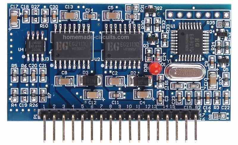
The driver board EGS002 was created especially for single-phase sinusoid inverters.
It makes use of an IR2110S driver chip and an ASIC EG8010 control chip.
Protection against voltage, current, and temperature is included into the driver board.
LEDs are used to indicate warnings, and fan control is included.
Jumpers enable the setting of dead time, soft start mode, and 50/60Hz AC output.
EGS002, which is an enhancement over EGS001, keeps the original interfaces of EGS001 compatible.
In addition, cross-conduction prevention logic is included into EGS002 for improved anti-interference performance.
For user convenience, an LCD display interface is provided, allowing the chip's integrated display capabilities to be used.
Here are some general datasheet for the EGS002:
General Datasheet
- Input voltage range: +15V - +20V DC and +5V
- Output voltage range: 110V or 220V AC (depending on the transformer used)
- Output frequency: 50Hz or 60Hz (depending on the configuration of the chip)
- Maximum output power: approximately 300W
- PWM frequency: 16kHz
- Over-current protection: Yes
- Over-voltage protection: Yes
- Under-voltage protection: Yes
- Over-temperature protection: Yes
- Standby power consumption: less than 1W
The EGS002 is designed to work with a center-tapped transformer, and can generate a pure sine wave output waveform using a combination of PWM and SPWM modulation techniques.
It has a low standby power consumption, high efficiency, and comprehensive protection features that make it suitable for small-scale renewable energy applications.
Note that these specifications are general and can vary depending on the specific implementation of the EGS002 inverter board.
It's always best to consult the datasheet or technical specifications provided by the supplier or manufacturer for the specific board you are working with.
Circuit Diagram for External MOSFETs
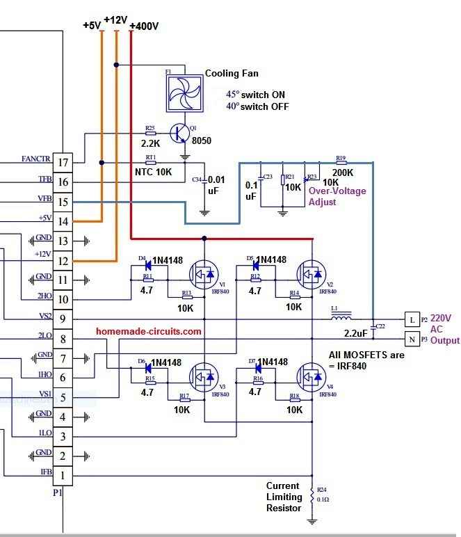
How to Connect
Connecting the EGS002 board to external MOSFETs is feasible, however it needs a few improvements to the board and good knowledge of the circuit design.
Listed below are the recommended methods to connect the EGS002 board to external MOSFETs:
Get rid of the present MOSFETs from the EGS002 board.
This would call for desoldering the MOSFETs from the board and eliminating any associated elements (for example gate resistors and diodes).
Choose the external MOSFETs that you would like to work with.
Ensure these are rated for the voltage and current specifications of your application.
Connect the gate of each external MOSFET to the equivalent gate drive signal on the EGS002 board.
The gate drive signals are generally named as "G" on the board.
Hook up the drain of each external MOSFET to the positive output of the center-tapped transformer.
The positive output of the transformer is normally attached to the positive terminal of the output capacitor.
Hook up the source of each external MOSFET to the negative output of the center-tapped transformer.
The negative output of the transformer is usually attached to the negative pin of the output capacitor.
Insert any essential elements to the circuit, for example gate resistors and diodes, to guarantee correct functioning of the MOSFETs.
Customize the control jumpers on the EGS002 board make it possible for external MOSFET functioning.
This might demand modifying the jumper settings for the "EGS002/04" and "EGS002/05" pins on the board, along with setting up the "EGS002/01" jumper to "ext".
It is critical to remember that changing the EGS002 board in this manner could be complicated and necessitates a great knowledge of the circuit design.
If you are not knowledgeable in electronics or inverter design, it's best to speak with an experienced person or work with a pre-built inverter board that actually contains external MOSFETs
LED Warning Indicator
The EGS002 driver board is equipped with an LED warning alert feature that assists users in identifying potential issues based on the following patterns:
- Normal Operation: The LED remains continuously illuminated.
- Overcurrent Condition: The LED blinks twice, then turns off for a 2-second interval, repeating in a cyclic manner.
- Overvoltage Situation: The LED blinks three times, followed by a 2-second off period, and then repeats this cycle.
- Undervoltage Problem: A sequence of four LED blinks occurs, succeeded by a 2-second pause, and the cycle continues.
- Overtemperature Issue: The LED blinks five times, pauses for 2 seconds, and maintains this cyclic pattern.
Pin Description and Working Details for EGS002
| PinOut | Name | I/O | Output Current Feedback/Descriptions |
|---|---|---|---|
| 1 | IFB | I | Pin voltage exceeding 0.5V triggers overcurrent protection |
| 2 | GND | GND | Ground |
| 3 | ILO | O | Right H-bridge Low side MOSFET gate driver output |
| 4 | GND | GND | Ground |
| 5 | VS1 | O | Right H-bridge high-side gate driver return path |
| 6 | 1HO | O | Right H-bridge High side MOSFET gate driver output |
| 7 | GND | GND | Ground |
| 8 | 2LO | O | Left H-bridge Low side MOSFET gate driver output |
| 9 | VS2 | O | Left H-bridge high-side gate driver return path |
| 10 | 2HO | O | Left H-bridge High side MOSFET gate driver output |
| 11 | GND | GND | Ground |
| 12 | +12V | +12V | +12V Input DC voltage input, can be between 10V-15V. |
| 13 | GND | GND | Ground |
| 14 | +5V | +5V | +5V DC supply |
| 15 | VFB | I | AC output voltage feedback to regulate the output voltage |
| 16 | TFB | I | Temperature monitored with overtemp protection at 4.3V pin voltage |
| 17 | FANCTR | O | Temperature-controlled fan. FANCTR turns the fan on (high output, 1) when above 45°C and off (low output, 0) below 40°C. |
Pinout for LCD Display Connection
| PinOut | Name | I/O | Description |
|---|---|---|---|
| *1 | +5V | Power Input | LCD power supply |
| *2 | GND | Ground | Ground connection |
| *3 | LCDDI | I/O | LCD serial data |
| *4 | LCDCLK | Output | LCD serial clock |
| *5 | LCDEN | Output | LCD chip select |
| *6 | LED+ | Power Input | Backlight power supply |
| *7 | LED- | Ground | Backlight ground connectionpen_spark |
Jumper Setting Details
| Designator | Name | Mark | JP jumper shorted selects [setting description] |
|---|---|---|---|
| 1 | FS0 | JP1 JP5 | JP1 shorted sets AC output to 60Hz Shorting JP5 sets the frequency to 50Hz |
| 2 | SST | JP2 JP6 | JP2 short enables 3s soft start JP6 short disables soft start |
| 3 | DT0 | JP3 JP7 | JP7+JP8 shorted: dead time 300ns JP3+JP8 shorted: dead time 500ns |
| 4 | DT1 | JP4 JP8 | JP4+JP7 shorted: dead time 1.0us JP3+JP4 shorted: dead time 1.5us |
| *5 | LED+ | JP9 | JP9 short: LCD backlight ON JP9 open: LCD backlight OFF |
Default Jumper Settings:
- Output Frequency: 50Hz (JP5 shorted)
- Soft Start: Enabled (JP2 shorted)
- Dead Time: 300ns (JP7 and JP8 shorted)
Jumper Customization:
These jumpers can be manipulated or changed as per users specific needs.
Note:
- Avoid Shorting Conflicting Jumpers: Only one jumper per function can be shorted at a time. For example, you cannot short both JP1 (60Hz) and JP5 (50Hz) simultaneously.
How to Test EGS002 Driver Board
Initial Setup
- Grounding Test Points: During testing, connect the following pins to ground: IFB, VS1, VS2, VFB, and TFB.
- Power Supply Connections:
- Connect +5V DC to the +5V pin.
- Connect +12V DC to the +12V pin (voltage range: 12V to 15V).
Testing Procedure:
Waveform Observation:
- Connect an oscilloscope to test points TEST1 through TEST4 to check the waveforms.
- TEST1 & TEST2: Output fundamental frequency square wave (appears as the blue CH1 waveform in Figure 5-3).
- TEST3 & TEST4: Output unipolar modulation wave. When connected to an RC filter, these points will output the waveform shown as the red CH2 waveform.
Undervoltage Protection Test:
- Since the VFB pin is grounded, the undervoltage protection will activate after 3 seconds.
- This will cause TEST1 through TEST4 to shut down.
- An LED will blink four times, then turn off for 2 seconds, and this cycle will repeat.
- Reconnecting the EGS002 to the power supply will allow you to observe waveforms for another 3 seconds before the undervoltage protection activates again.