For a beginner in electronics, constructing basic electronic projects from a circuit diagram could be overwhelming. This quick guide is intended to assist newbies by enabling them handy details about electronic parts as well as regarding techniques of building circuits. We will examine elementary parts like resistors, capacitors, inductors, transformers and potentiometers.
RESISTORS

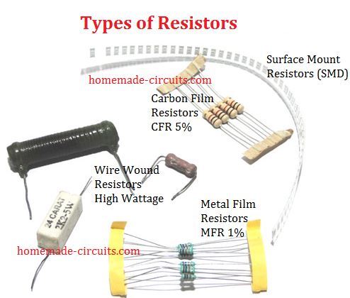
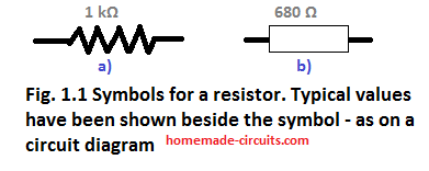
A resistor is a part that dissipates power, normally through heat. This dissipation process can be defined by the relationship known as Ohm's law: V=I X R where V is the voltage over the resistor in volts, I refers to the current through the resistor in amps and R is the resistor value in ohms. The symbols for a resistor which are normally used schematics are shown in the following Fig. 1.1.
Resistors can be used in two basic ways in an electronic circuit. We can use a resistor either to alter the voltage at a specific location in the circuit, or to change the current at a desired location of the circuit.
The resistor's value may be identified through the colored rings around it. You will find 3 fundamental rings or bands that enlightens us with the following details (Fig. 1.2).
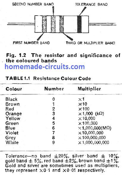
The bands are painted with specific colors and each colored band represents a number as revealed in the above Table 1.1. As an example when the bands are brown, red and orange, then the value of the resistor will be 12 X 1,00.0 or 12,000 ohms; 1,000 ohms is normally identified as a kilohm or k, while 1,000,000 is named a megohm or MOhm.
The last colored ring or band signifies the tolerance magnitude of the resistor, for the particular resistor value. Gold reveals a + or - 5 per cent (±5%) tolerance, silver signifies that it is + or - 10 per cent (±10%).
If you find no tolerance band present will usually means that the tolerance is ±20 per cent.
Generally speaking, the bigger the resistor, the greater power it may be rated to handle. The power rating in watts may differ from 1/8 W up to many watts. This power is basically the product of voltage (V) and current (I) passing through the resistor.
Applying Ohm's law we can determine the power (P) dissipated by a resistor as P = V X I = I2R = V2/R where R is the value of the resistor. You won't find any electrical disadvantage if your resistor has higher wattage or power rating than the required specifications.
The only slight drawback could be in the form of an increased mechanical dimensions and perhaps higher costs.
CAPACITORS
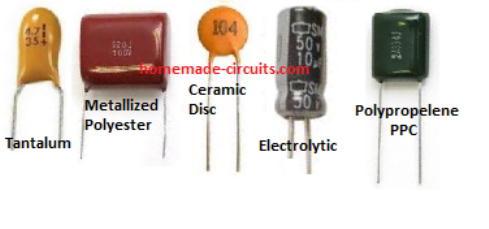
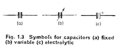
The earlier name for any capacitor used to be condenser, though the present name looks more related to its actual function. A capacitor is designed with a "capacity" for storing electrical energy.
The basic function of a capacitor is to allow the passage of an alternating current (a.c.) through it but block a direct current (d.c. ).
Another crucial thing about a capacitor is that in case a d.c. voltage, from example through a battery, is connected across a capacitor for a moment, this DC will be stored and continue to be remain across the capacitor leads until either an element like a resistor is joined across its leads, or may be you eventually short the leads with causing the stored energy to discharge.
CONSTRUCTION
Generally, a capacitor is made of a pair of plates separated by an insulating substance known as the dielectric.
The dielectric could be formed by air, paper, ceramic, polystyrene or any type of different appropriate material. For bigger capacitance values, an electrolyte is employed for the dielectric separation. This electrolytic substance has the ability to store electrical energy with great efficiency.
A constant DC is normally required for proper functioning of all electrolytic capacitors, simply because these are polarized in nature. That is why in circuit diagrams we find the positive lead of the capacitor indicated as a white block while the negative side as a black block.
Variable or adjustable capacitors include turning vanes separated by an air gap or an insulator such as mica. How much these vanes overlap each other determines the magnitude of the capacitance, and this can be varied or adjusted by moving the spindle of the variable capacitor.
Capacitance is measured in Farads. However, a one Farad capacitor could be substantially large for any practical use. Therefore , capacitors are designated either in microfarads (uF), nanofarad (nF) or in picofarads (pF).
A million picofarads corresponds to a single microfarad, and a million microfarads equals one Farad in magnitude.
Although nanofarads (nF) are not used very often, one nanofarad represents a thousand picofarads.
Occasionally you may find smaller capacitors with color codes marked on them, just like the resistors.
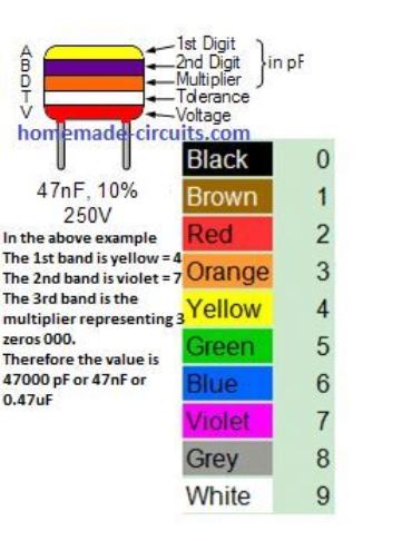
For these, the values could be determined in pF as demonstrated in the above color chart. The pair of bands at the bottom provides the tolerance and maximum workable voltage of the capacitor.
It must be strictly noted that the voltage rating printed on the capacitor body represents the absolute maximum tolerable voltage limit of the capacitor which must never be exceeded. Also, when electrolytic capacitors are involved, the polarity must be carefully checked and soldered accordingly.
INDUCTORS
In electronic circuits Inductor working characteristics are just the opposite of capacitors.
Inductors show the tendency to pass a direct current through them but try to oppose or resist alternating current. They are usually in the form of super enameled copper wire coils, normally wound around a former.
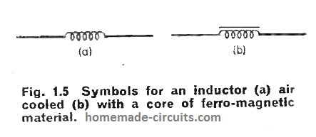
For creating high value inductances, a ferrous material is normally introduced as the core, or may be installed like a cover surrounding the coil externally.
An important characteristic of the inductor is its ability to generate a "back e.m.f." as soon as an applied voltage is removed across an inductor. This normally happens due to the inherent feature of an inductor for compensating the loss of the original current across current.
The schematic Symbols of inductor can be seen in the Fig. 1.5 below. The unit of inductance is the Henry, although millihenrys or microhenrys (mH and respectively) are normally used for measuring inductors in practical applications.
One millihenry has a 1000 microhenry while a thousand millihenrys equals one Henry. Inductors are one of those components that are not easy to measure especially if the actual value is not printed. Also these become even more complex to measure when these are constructed at home using non-standard parameters.
When inductors are used for blocking AC signals, they are called radio frequency chokes or RF chokes (RFC).
Inductors are used with capacitors to form tuned circuits, which allow only the calculated band of frequencies to pass through them, and block the rest.
TUNED CIRCUITS
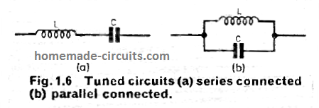
A tuned circuit (Fig. 1.6), which involves an inductor L and a capacitor C, will, essentially, either allow a particular frequency to move across and block all other frequencies, or block a specific frequency value and let all the other to pass through.
A measure of the selectivity of a tuned circuit which ascertains the frequency value becomes its Q (for quality) factor.
This tuned value of the frequency is also termed as the resonant frequency (f0) and is measured in hertz or cycles per second.
A capacitor and inductor may be used in series or in parallel to form a resonant tuned circuit (Fig. 1.6.a). A series tuned circuit may have a low loss compared to a parallel tuned circuit (Fig. 1.6.b) which may have a high loss.
When we mention loss here, it usually refers to the ratio of voltage across the network, to current flowing through the network V/I. This is also known as its impedance (Z).
The alternative names for this impedance (Z) for specific components may be in the form of e.g. resistance (R) for resistors and reactance (X) for inductors and capacitors.
TRANSFORMERS
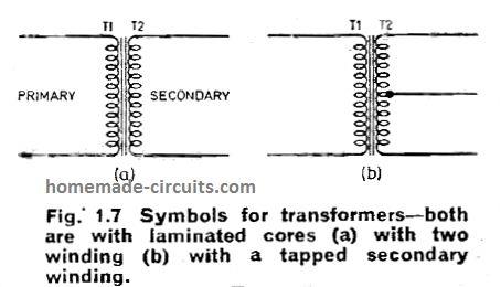
Transformers are used for stepping up an input alternating voltage/current to higher output levels or for stepping down the same into lower output levels. This working also simultaneously ensures a complete electrical isolation across the input AC and the output AC. A couple of transformer topologies can be witnessed in below Fig. 1.7.
Manufactures signify all the details on the primary, or input side through the suffix "1". The secondary, or output side, is signified by the suffix "2"; T1 and T2 indicate the amount of turns on the primary and secondary correspondingly. Then:
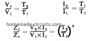
When a transformer is designed for stepping down mains 240 V to a lower voltage, say 6 V, the primary side involves relatively higher number of turns using thinner gauge wire while the secondary side is built using relatively lesser number of turns but using much thicker gauge wire.
This is due to the fact that the higher voltage involves proportionately lower current and therefore thinner wire, while the lower voltage involves proportionately higher current and therefore thicker wire. The net primary and secondary wattage values (V x I) is almost equal in an ideal transformer.
When the transformer winding has a wire tapping extracted from one of the turns (Fig. 1.7.b), results in the division of the winding voltage across the tapping which is proportionate to the number of turns on the winding separated by middle tapped wire.
The net voltage magnitude across the full end to end secondary winding will still be according to the formula shown above
How big a transformer may be depends on the magnitude of its secondary current specification. If the current spec is bigger the transformer dimensions also gets bigger proportionately.
There are also miniature transformer designed for high frequency circuits, like radios, transmitters etc and they have an in-built capacitor attached across the winding.
How to Use Semiconductors in Electronic Projects
By: Forest M. Mims
Building and experimenting with electronic projects can be rewarding, but a lot challenging. It becomes even more satisfying, when you as a hobbyist finish building a circuit project, power it on, and find a useful working model developed from handful of junk components. This, makes you feel like a creator, while the successful project exhibits your tremendous efforts and knowledge in the respective field.
This may be just for having some fun in the leisure time. Some other folks might want to accomplish a project that's not yet manufactured, or may be customize a market electronic product into a more innovative version.
For achieving success or to troubleshot a circuit fault, you will have to be well versed regarding the working of the various components and how to implement correctly in practical circuits. OK, so let's come to the point.
In this tutorial we'll begin semiconductors.
How Semiconductor is Created using Silicon
You will find a variety of semiconducting components, but silicon, which is the principle element of sand, is among the most well-known element. A silicon atom consists of just 4 electrons within its outermost shell.
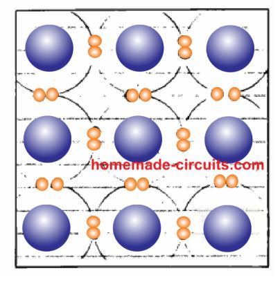
However it may well love to get 8 of them. As a result, a silicon atom collaborates with its neighboring atoms to share electrons in the following manner:
When a group of silicon atoms share their outer electrons, it results in the formation of an arrangement known as crystal.
The drawing below shows a silicon crystal having only their outer electrons. In its pure form silicon does not provide a useful purpose.
Because of this reason, manufacturers enhance these silicon based items with phosphorous, boron, and additional ingredients. This process is called "doping" of silicon. Once doping is implemented silicon it gets enhanced with useful electrical properties.
P and N Doped Silicon: Elements like Boron, phosphorous, can be effectively used for combining with silicon atoms to manufacturing crystals. Here's the trick:
A boron atom includes just 3 electrons in its outer shell, while a phosphorus atom includes 5 electrons.
When Silicon is combined or doped with some phosphorus electrons it transforms into n -type silicon (n = negative). When Silicon is fused with boron atoms which lacks an electron the silicon gets turned into a p -type (p= positive) silicon.
P-type Silicon: When boron atom is doped with a cluster of silicon atoms it gives rise to a vacant electron cavity called a "hole."
This hole makes it possible for an electron from an neighboring atom to "drop" into the slot (hole). This means, one "hole" has changed its position to a new location. Keep in mind, holes can easily float across silicon (in the same way bubbles move on water).
N-Type Silicon: When a phosphorus atom is combined or doped with a cluster of silicon atoms, the system gives an extra electron that is allowed to transfer across the silicon crystal with relative comfort.
From the above explanation we understand that an n-type silicon will facilitate the passage of electrons by causing electrons to jump from one atom to the other.
On the other hand a p-type silicon will also enable the passage of electrons but in the opposite direction. Because in a p-type, it is the holes or the vacant electron shells that are causing the relocation of the electrons.
Human Analogy: It's like comparing a person running on the ground, and a person running on a treadmill. When a person runs on ground the ground remains stationery, and the person moves ahead, while on treadmill the person remains stationery, the ground moves backwards. In both the situations, the person is going through a relative forward movement.
Understanding Diodes
Diodes can be compared to valves, and thus play a crucial role in electronic projects for controlling the direction of flow of electricity within a circuit configuration.
We know that both n and p type silicon have the ability to conduct electricity. The resistance of both variants depends upon the percentage of holes or the extra electrons it owns. As a result, the two types may be also able to behave like resistors, restricting current and allowing it to flow only in a specific direction.
By creating many p-type silicon inside a base of n-type silicon, electrons can be restricted to move across the silicon in just one direction. This is the exact working condition that can be witnessed in diodes, created with a p-n junction silicon doping.
How the Diode Works
The following illustration helps us to get an easy clarification regarding how a diode responds to electricity in a single direction (forward) and ensures blocking electricity in the opposing direction (reverse).
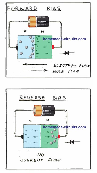
In the first figure, the battery potential difference causes holes and electrons to repel toward the p-n junction. In case the voltage level goes over 0.6 V (for a silicon diode), electrons become stimulated to jump across the junction and fuse with the holes, making it possible for a current charge to transfer.
In the second figure, the battery potential difference causes the holes and the electrons to get pulled away from the junction. This situation prevent the flow of charge or current blocking its path.
Diodes are typically encapsulated in tiny cylindrical glass casing.
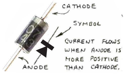
A darkish or whitish circular band marked around one end of the diode body identifies its cathode terminal. The other terminal naturally becomes the anode terminal. The above image demonstrates both the physical encasing of the diode and also its schematic symbol.
We, by now have understood that a diode can be compared to an electronic one way switch. You still need to fully grasp a few more factors of diode functioning.
Below are a few crucial points:
- A diode may not conduct electricity until the applied forward voltage reaches a particular threshold level.For silicon diodes, it is approximately 0.7 volt.
- When the forward current becomes too high or above the specified value, the semiconductor diode might bust or burn! And the internal terminal contacts could disintegrate.
- If the unit burns, the diode may all of a sudden show conduction across both the terminal directions. The heat generated due to this malfunction may eventually vaporize the unit!
- Excessive reverse voltage may result in a diode to conduct in the opposite direction. Because this voltage is pretty large, the unexpected current surge may crack the diode.
Diode Types & Uses
Diodes are available in many different forms and specs. Below are some of the important forms that are commonly used in electrical circuits:
Small Signal Diode: These types of diodes can be used for low-current ac to dc conversion, for detecting or demodulating RF signals, in voltage multiplier application, logic operations, for neutralizing high voltage spikes, etc. for making Power Rectifiers. Example, 1N914, 1N4148 etc
Medium Power Diode: These are normally rated to handle and rectify moderate amounts of current normally within the range of a few hundred mA to many amps. Example: 1N4007, 1N5402, iN5408, 6A4
Power rectifiers Diodes: have similar attributes and characteristics like a small and medium power diode, but these are rated to handle significant magnitudes of current. These are mounted over big metal enclosures that help absorb and dissipate unwanted heat and distribute it across an attached heatsink plate. Example: NTE5991
Power diodes can be also used for making AC to DC rectifiers which can be mostly seen in power supply units. Common variants are 1N4007, 1N5402/5408, 6A4 etc
Zener Diode: This is a special type of diode characterized with a specific reverse breakdown voltage. Meaning, zener diodes can work like a voltage-limiting switch. Zener diodes are rated with absolute breakdown voltages (Vz) that may range from 2 to 200 volts.
Light-Emitting Diode or LEDs: All forms of diodes have the property of emitting a bit of electromagnetic radiation when applied to a forward bais voltage.
However, the Diodes that are created using semiconductors materials like gallium arsenide phosphide get the ability of emitting significantly more amount of radiation compared to the regular silicon diodes. These are called Light Emitting Diodes or LEDs.
Photodiode: Just as diodes emit some radiation, they also exhibit some level of conduction when illuminated by an external light source.
However the Diodes that are specially designed to detect and respond light or illumination are called photodiodes.
They incorporate a glass or plastic window which allows the light to enter the diode's light sensitive area.
Typically these have large, junction area for the required exposure to light.
Silicon facilitates the making of efficient photodiodes.
Different types of diodes are widely-used in a great many applications. For the time being, let us discuss a couple of important functions for small signal diodes and rectifiers:
The first is a single wave rectifier circuit through which an alternating current with a varying dual polarity supply is rectified into a single polarity (dc) signal or voltage.
The second configuration is the full-wave rectifier circuit which comprises a four-diode configuration and is also termed as bridge rectifier. This network has the ability for rectifying both halves of an AC input signal.
Observe the distinction in end result from the two circuits. In the half-wave circuit just one cycle of the input AC produces an output, while in full bridge both the half cycles are transformed into a single polarity DC.
The Transistor
An electronic project can be virtually impossible to complete without a transistor, which actually forms the basic building block of electronics.
Transistors are semiconductor devices having three terminals or leads. An exceptionally tiny amount of current or voltage on one of the leads allows the control of a significantly larger amount of current flow across the other two leads.
This implies that, transistors are best suited to work as amplifiers and switching regulators. You will find two primary groups of transistors: bipolar (BJT) and field-effect (FET).
In this discussion We are going to focus just on bipolar transistors BJT. Put simply, by adding a complementing junction to a p-n junction diode it becomes possible to create a 3 compartment silicon "sandwich." This sandwich like formation can be either n-p-n or p-n-p.
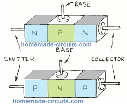
In either case, the midsection region works like a tap or control system that regulates the quantity of electrons or charge shifting across the 3 layers. The 3 sections of a bipolar transistor are the emitter, base, and collector. The base region can be quite thin and it has much less doping atoms compared to emitter and collector.
As a result, a much smaller emitter-base current results in a significantly bigger emitter-collector current to move. Diodes and transistors are similar in nature with many of their crucial properties:
The base-emitter junction which resembles a diode junction will not allow electron transfer unless the forward voltage goes beyond 0.7 volt. Excessive amount of current causes heating up of the transistor and perform inefficiently.
In case a transistor temperature rises significantly it may be required to power off the circuit! Eventually, an excessive amount of current or voltage may cause a permanent damage to the the semicondictor material which constitutes the transistor.
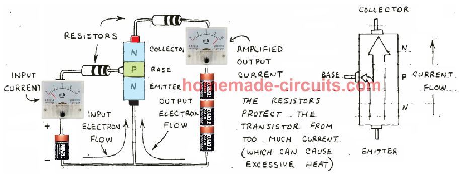
Various sorts of transistors can be found today. Common examples are:
Small Signal and Switching Transistors: These transistors can be used for amplifying low level input signals to a relatively larger levels. Switching transistors are configured either to switch ON fully or switch Off fully. All types of transistors can be used for both the functions, that is for amplifying and switching input signals equally well.
Power Transistor: These transistors are employed in high power amplifiers and power supplies. These transistors are typically Large sized and with extended metal casing to facilitate greater heat dissipation and cooling, and also for easy installation of heatsinks.
High-Frequency: These transistors are mostly used RF based gadgets such as radios, TVs, and microwaves. These transistors are built with thinner base region, and have reduced body dimenions. The schematic symbols for the npn and pnp transistors can be witnessed below:
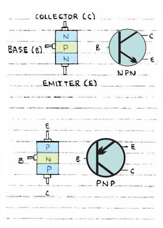
Remember that the arrow sign in the transistor symbol as shown above indicates the emitter pin which always points towards the flow direction of holes. When the arrow sign shows a direction that's opposite from the base, then the BJT has an emitter consisting of n-type material.
This sign specifically identifies the transistor as an n-p-n device with base having a p-type material. On the other hand, when the arrow mark is pointing towards the base, that indicates base is made up of n-type material, and indicates that the emitter and collector both consist of p-type material and, as a result, the device is a pnp BJT.
How to Use Bipolar Transistors
When a ground potential or 0V is applied to the base of an npn transistor, it inhibits the flow of current across the emitter-collector terminals and the transistor is rendered switched "off."
In case the base is forward-biased by applying a potential difference of at least 0.6 volt across the base emitter pins of the BJT, it instantly initiates the flow of current from the emitter to the collector terminals and the transistor is said to be switched "on."
While BJTs are powered in only these two methods, the transistor operates like an ON/OFF switch. In case the base is forward-biased, the emitter-collector current magnitude becomes dependent on the relatively smaller variations of the base current.
The transistor in such cases works like an amplifier. This particular topic relates to a transistor where the emitter is supposed to be the common ground terminal for the input and the output signal both, and is referred to as common-emitter circuit. A few basic common-emitter circuits can be visualized through the following diagrams.
Transistor as a Switch
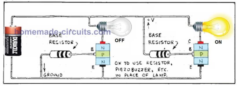
This circuit configuration will accept only two types of input signal, either a 0V or ground signal, or a positive voltage +V above 0.7V. Therefore, in this mode the transistor can be either switched ON or switched OFF. The resistor at the base could be anything between 1K and 10K ohms.
Transistor DC Amplifier
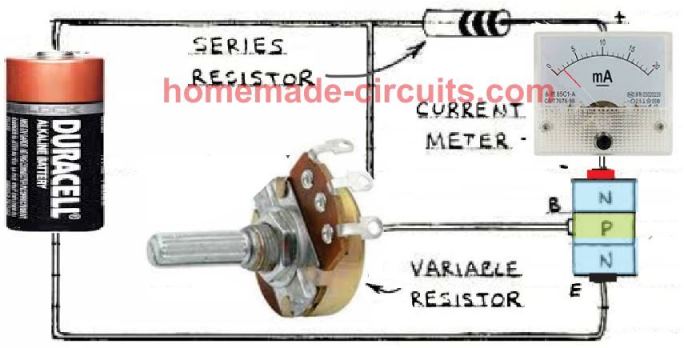
In this circuit the variable resistor creates a forward biasing to the transistor and regulates the magnitude of base/emitter current. The meter shows the amount of current delivered across the collector emitter leads.
The meter series resistor ensures safety to the meter against excessive current, and prevents damage to the meter coil.
In a real application circuit the potentiometer can be added with a resistive sensor, whose resistance varies in response to an external factor such as light, temperature, moisture etc.
However, in situations where the input signals varies rapidly, an AC amplifier circuit becomes applicable as I have explained below:
Transistor AC Amplifier
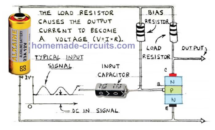
The circuit diagram shows a very basic transistorized AC amplifier circuit. The capacitor positioned at the input blocks any form of DC from entering the base. The resistor applied for the base bias is calculated to establish a voltage that's half the supply level.
The signal which is amplified "glides" along this constant voltage and changes its amplitude over and under this refrence voltage level.
If the biasing resistor was not used, only half the supply above 0.7V level would get amplified causing high amounts of unpleasant distortions.
Regarding the Direction of Current
We know that when electrons travels through a conductor, it generates a flow of current through the conductor.
Since, technically the movement of electrons is actually from a negatively charged region to positively charged region, then why do the arrow mark in a diode symbol appear to indicate an opposite flow of electrons.
This can be explained with a couple points.
1) As per the initial theory by Benjamin Franklin, it was assumed that the flow of electricity is from positive to the negative charged region. However, once electrons were discovered, it revealed the actual truth.
Still, the perception continued to remain the same, and the schematics continued to follow the conventional imagination in which the current flow is shown from positive to negative, because somehow thinking the opposite makes us difficult to simulate the results.
2) In case of semiconductors, it is actually the holes that travel opposite to the electrons. This make the electrons appear to be shifting from positive to negative.
To be precise, it must be noted that the flow of current is actually the flow of charge created by the presence or the absence of the electron, but as far as electronic symbol is concerned we simply find the conventional approach easier to follow,
The Thyristor
Just like transistors, thyristors are also semiconductor devices that have three terminals and play an important role in many electronic projects.
Just as a transistor switches ON with a small current at one of the leads, thyristors also work in the similar fashion and enable a lot bigger current to conduct via the other two complementing leads.
The only difference is, thyristor do not have the ability to amplify oscillating AC signals. They respond to the control input signal by either turning fully on or fully off. This is the reason why, thyristors are also known as "solid-state switches."
Silicon-Controlled Rectifiers (SCR)
SCRs are devices that represent two basic forms of thyristors. Their structure resemble that of a bipolar transistors but SCRs have a fourth layer, hence three junctions, as illustrated the following figure.
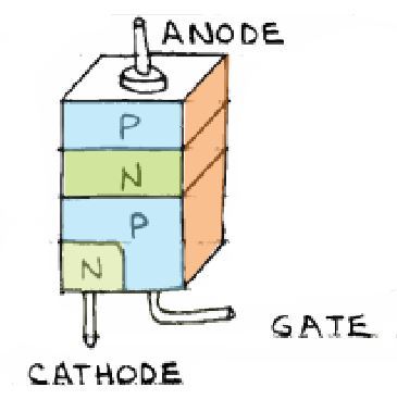
The SCR internal layout and schematic symbol can be visualized in the following image.

Normally, SCR pinouts are shown with single letters as: A for anode, K (or C) for cathode, and G for gate.
When the anode pinA of an SCR is applied with a positive potential that's higher than the cathode pin (K), the two outermost junctions become forward biased, although the central p-n junction stays reverse biased inhibiting any flow of current through them.
However, as soon as the gate pin G is applied with a minimal positive voltage, it allows a much larger power to conduct through the anode/cathode pins.
At this point, the SCR gets latched and the remains switched ON even after the gate bias is removed. This may continue infinitely until the anode or the cathode is momentarily disconnected from the supply line.
The next project below shows an SCR configured like a switch for controlling an incandescent lamp.
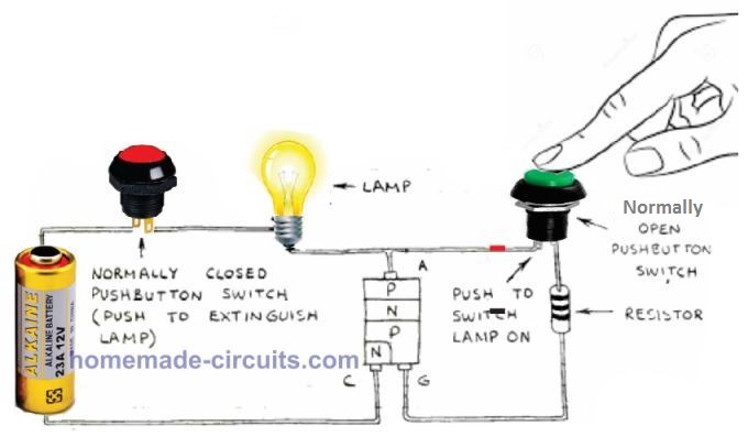
The left side switch is a push-to-OFF switch meaning it opens when pushed, while the right side switch is a push-to-ON switch which conducts when pressed. When this switch is pressed momentarily or just or a second, it switches ON the lamp.
The SCR latches and the lamp switches ON permanently. To switch OFF the lamp to its initial condition, the left side switch is pressed momentarily.
SCRs are manufactured with different power ratings and handling capacity, right from 1 amp, 100 volts to 10 amps or higher and several hundreds of volts.
Triacs
Triacs are specifically used in electronic circuits that require high voltage AC load switching.
The internal structure of a triac actually looks like two SCRs joined in reverse parallel. This means a triac gets the ability to conduct electricity in both the directions for DC as well as AC supplies.
To implement this feature the triac is built using five semiconductor layers with an extra n-type region. The triac pinouts are connected such that each pin comes in contact with a pair of these semiconductor region.
Although the working mode of a triac gate terminal is similar to an SCR, the gate is not specifically referenced to anode or cathode terminals, it is because the triac can conduct both ways so the gate can be activated with any of the terminals depending on on whether a positive signal is used or a negative signal for the gate trigger.
Due to this reason the triac's two main load carrying terminals are designated as MT1 and MT2 instead of A or K. The letters MT refers to "main terminal." as shown in the following circuit diagram.
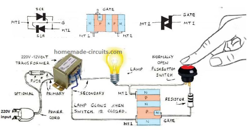
When a triac is applied for switching an AC, the traic conducts only as long as the gate remains connected to a small supply input. Once the gate signal is removed it still keeps the triac switched ON but only until the AC waveform cycle reaches the zero crossing line.
Once the AC supply reaches the zero line the triac switches OFF itself and the connected load permanently, until the gate signal is applied yet again.
Triacs can be used for controlling most domestic appliances along with motors and pumps.
Although triacs are also categorized as per their current handling capacity or rating like SCRs, SCRs are generally available with much higher current ratings than a triac.
Semiconductor Light Emitting Devices
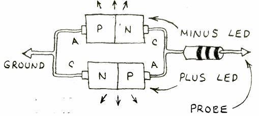
When exposed to high levels by light, heat, electrons, and similar energies, most semiconductors show the tendency of emitting light at human visible wavelength or IR wavelength.
The semiconductors which are ideally suitable for this are the ones that come in the family of p-n junction diodes.
Light-emitting diodes (LED) do this by converting electrical current directly into visible light. LED are extremely efficient with its current to light convresion than any other form of light source.
White high bright LEDs are used for home illumination purposes, while the colorful LEDs are used in decorative applications.
The LED intensity can be controlled either by linearly decreasing the input DC or through pulse width modulation input also called PWM.
Semiconductor Light Detectors
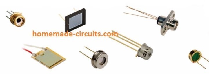
When any form of energy comes in contact with a semiconductor crystal it leads to the generation of a current in the crystal. This is the basic principle behind the working of all semiconductor light sensor devices.
Semiconductor light detectors can be categorized into into main types:
The ones that are built using pn junction semiconductors and the other which are not.
In this explanation we will only deal with only the p-n variants. P-n junction based light detectors are the most widely used member of the photonic semiconductor family.
Most are made from silicon and can detect both visible light and near -infrared.
Photodiodes:
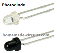
Photodiodes are specially designed for electronic projects which are designed for sensing light. You can find them in all sorts of gadgets such as in cameras, burglar alarms, LiFi communications, etc.
In the light detector mode a photo-diode works by generating a hole or electron sharing at a pn junction. This causes current to move as soon as the p and the n junction side terminals are connected to an external supply.
When used in the photovoltaic mode, the photodiode acts like a current source in the presence of an incident light. In this application the device begins operating in the reverse bias mode in response to a light illumination.
In the absence of light, a minute amount current still flows known as "dark current".
A photodiode generally is manufactured in many different packaging designs . They are mostly available in plastic body, pre-installed lens and filtration, and so forth.
The key differentiation is the dimension of the semiconductor which is used for the device. Photodiodes intended for high speed response times in the reverse bias photoconductive operation are built using small area semiconductor.
Photodiodes with larger area tend to respond a little slow, but may have the ability to deliver higher degree of sensitivity to the light illumination.
The photodiode and the LED share identical schematic symbol, except that the direction of the arrows which are inwards for the photodiode. Photodiodes are typically accustomed to recognize rapid varying pulses even at near infrared wavelength, as in lightwave communications.
The below circuit illustrates the way the photodiode could possibly be applied in a light-meter set up. The output results of this circuit is quite linear.
Phototransistors
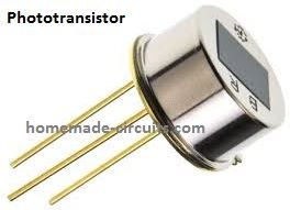
Phototransistors are applied in electronic projects that require higher degree of sensitivity. These devices are exclusively created to to exploit it sensitivity to light feature in all transistors. In general a phototransistor can be found in an npn device having a broad, base section which can be exposed to light.
Light getting into the base takes the place of the natural base-emitter current that exists in normal npn transistors.
Due to this feature, a phototransistor is able to amplify the light variations instantly. There are typically two types of npn phototransistors that can be obtained. One is with a standard npn structure, the alternative variant comes with an additional npn transistor to offer added amplification, and is known as a "photodarlington" transistor.
These are extremely sensitive, although a bit sluggish compared to regular npn phototransistor. The schematic symbols generally employed for phototransistors are as given below:
Phototransistors are quite often applied to detect alternating (ac) light impulses. They are in addition utilized to identify continuous (dc) light, such as the following circuit where a photodarlington is applied to activate a relay.
This tutorial will be regularly updated with new components specifications, so please stay tuned.
Hello my friend! I really like the work you do here. I am a beginner and would like to know if you could indicate a learning sequence through the pages available here. I have multimeter, power supply, protoboard, some components. I’m here from Brazil, if you can show me a way to learn, I would be very grateful. Success and congratulations on the work you do! Denis Araujo vianamusic2011@hotmail.com
Thank you Denis,
To learn electronics you will first have to master the transistors or the BJTs. Therefore, you can start by the basic understanding of how to use a BJTs, as explained in the following article.
https://www.homemade-circuits.com/how-to-understand-and-use-transistors/
You can also learn about relays and how to drive them using a transistor
https://www.homemade-circuits.com/how-a-relay-works-in-circuits-how-to-connect-it/
https://www.homemade-circuits.com/how-to-make-relay-driver-stage-in/