In this post I have explained some important current mirror circuits, and how to design practical circuits using current mirror concepts.
Current Mirror Definition
A current mirror is a circuit that copies a current through one active device by regulating the current in another active device in the circuit, maintaining a constant output current independent of load. The active devices are generally two BJTs or two MOSFETs
Basic Current Mirror Circuit
Observe that Q1's collector is shorted to its base in the basic current mirror circuit depicted in the following figure. This is known as a diode-connected transistor.

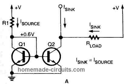
Q1 is still very much in "active" operating mode because the collector to base voltage is zero. Furthermore, connecting the bases and emitters of Q1 and Q2 results in their sharing the same base-emitter voltage.
For a silicon transistor, resistor R1 provides a fixed-bias current to Q1, yielding a base-emitter voltage of roughly 0.6 volts. Q2 is biased into conduction by this voltage.
For a moment, we'll suppose that the base-emitter voltage and gain of both transistors are perfectly matched, and that the current gain is exceptionally high. Because the base-emitter voltages for Q1 and Q2 are identical, the base and emitter currents are also identical.
When Q2 has a load inside its "compliance" range, the collector currents across both transistors are precisely identical, which is the most important aspect of the circuit. The base currents are insignificant with such a large gain, and the collector current of Q2 matches the current through Q1.
We can say that the source current from R1 is "mirrored" by Q2 assuming conventional flow of current (flow of electron from a positive terminal to a negative terminal) to explain the circuit response. Q2 sinks the identical amount of current at its collector as Q1. As a result, this form of circuit is referred to as a "current mirror".
Transistor Q2's "compliance" range, where its sink current is identical to its source current, could be anywhere between +V and 0.6 volts. Q2's collector-base junction would have a negative bias if the voltage decreases under 0.6 volts.
For example, shorting Q2's collector to +V, or employing a resistive load of adequate value to decrease +V to 0.6 volts at the load (or source) current determined by R1 are also feasible options. R1's value can be calculated by the formula:
R1 = ( +V - 0.6V) /Isink
Naturally, the transistors used must be capable of handling the required current. The base-emitter voltage (0.6 V) that Q1 and Q2 share is a "singularity" on its own, in the fundamental current mirror circuit. Regardless of what we do to the output circuit at Q2 by using ideal parts and matching, the singularity would not alter. No matter whatever load, it maintains its predicted voltage.
One example is the circuit indicated in the following figure.
Current Mirror as Current Sink
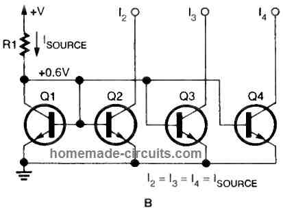
In tandem with Q2, transistors Q3 and Q4 have been introduced. Along with Q2, each of the extra transistors may now sink the identical amount of current. We may now sink a current three times the quantity of the input source current by interconnecting the collectors of Q2, Q3, and Q4 as illustrated in the figure below indicated below.
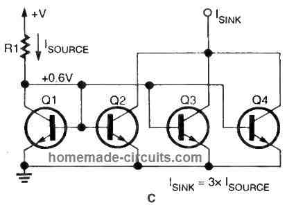
This is because, since the "composite" transistors Q2-Q3-Q4 now have 3 times the silicon area of a single transistor.
Thus, while building integrated circuits, current mirrors employ transistors having variable chip areas to produce varying levels of current throughout the IC. This is common in "current-steering" circuits. The current mirror is an excellent current sink (when used with NPN devices) or source (with PNP units). Either circuit can be simply built on a monolithic chip.
It may appear to be an "optimal" circuit at this point, enabling a huge number of paralleled outputs with flawless performance.
In reality, however, this never happens. As we shall see in the next breadboard tests, parameters including base-emitter voltage and gain matching, temperature monitoring, and output resistance all have varying degrees of influence on circuit efficiency. In addition, we will demonstrate some circuit adjustments that will greatly enhance our findings.
How to Design Current Mirrors
Standard discrete transistors are the ideal place to begin our explorations. A tiny solderless breadboard, a basic 9-volt battery, several 1/4-watt resistors, and a couple of transistors are all that is required.
You're all set to go if you already have a bunch of general-purpose transistors with identical part number. If not, NPN variants like the 2N3904 or 2N2222 can be obtained cheaply packaged in 10 or 15 piece packs. Likewise, PNP variants like the 2N3906 and 2N2907 are also easily available in the market.
In our first experiment, we'll try to associate two separate transistors together. Possibly, from out of ten pieces, you may be able to strike a great combo! Legitimate results, on the other hand, do not require a good match.
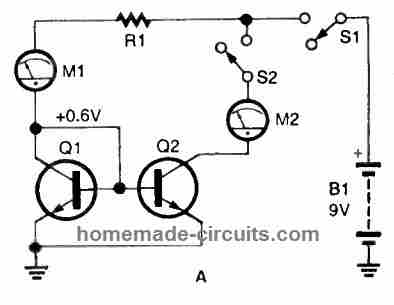
Build the basic current-mirror circuit over a breadboard, utilizing 22-gauge solid-wire jumpers wherever appropriate, as shown below in Fig. A for NPN devices, and Fig. B for PNP BJTs.
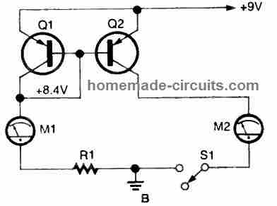
Starting with an 8200 ohm value for R1, the input reference current would be:
(9.0 volts - 0.6 volts) /8200 ohms or approximately 1 mA.
Apply voltage to the circuit and hook up ammeter M1 in series with R1. Take the reading of the current measurement. Repeat the procedure by changing R1 to 82,000 ohms. We would now observe a reading of around 100 microamps; make a note of that as well.
Remove M1 from the circuit and reconnect R1. Measure the voltage drop between the base-emitter junctions of Q1 and Q2 with Q2's collector pin in the open condition, which should be around 0.6 volts. Q2's collector should be connected to +V (for the NPN type) or ground (for the PNP type).
You might find the base-emitter voltage drop increased by 10 to 20 mV. This is due to transistors limited gain and output resistance, that have non-standard specs in the physical realm. We'll explain you the effects of such an increase soon.
Attach M2 in series with Q2's collector terminal (obviously, using an ammeter) and record the output current with R1 at 82,000 ohms.
Now, a measurement in the range of 100 microamps should be seen. Replace a different transistor for Q2 with identical number. Take note of the output current once more. Allow the circuit temperature to normalize after handling any of the transistors, to ensure accurate readings.
Connect the previous original transistor to the existing Q2 and record the output current, that should be equivalent to the total of your earlier observations.
Return to one unit for Q2 and repeat the process with another few BJTs to check if you can locate a transistor which matches Q1. If you are able to achieve within 10% or 20% of the target, consider yourself lucky!
Modify R1 again to 8200 ohms for a 1 mA reference current as soon as you've found the "closest match."
The reference current is minimally affected by the voltage drop, while the output current is substantially affected!
Touch Q2 with your finger now, and observe the inverse result: the output current increases fast as Q2's effective bias threshold falls, but the net base/emitter voltage, as well as the reference current, stay constant.
Implementing discrete BJT devices, temperature monitoring across both transistors becomes obviously a major issue. Using a common heatsink or even gluing the BJTs together of course, benefits a lot.
The ideal solution, nevertheless, is to employ components that were manufactured along the same substrate and packaged together. Afterwards, we'll go over this method in further detail.
We'll now try to learn the implications of finite gain and output resistance employing our "matching" circuit discussed above. Check the output current once the temperatures of both transistors have settled, and noting that it is around 1 mA.
R2 now could be added to the circuit, as illustrated in the below Fig. C, which is the NPN form of the circuit.
R2 is introduced in the same way if you're dealing with the PNP variant of the circuit. R2 should be set to 1000 ohms. Take note of the current output.
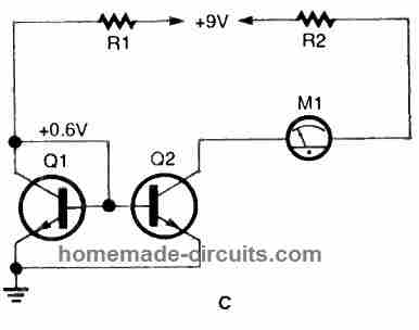
Next, increase R2's value by roughly 2000 ohms and record the output current once more. Continue to increase R2's value while measuring the output current until you achieve around 7500 ohms. At this present level, the transistors must be close to their optimum compliance voltage.
With common transistors, the output current drops by 20% or so when the value of R2 is raised across the compliance range. The circuit in parallel with R2 has a low output impedance, which causes this.
Ideal Current Source
For a genuine constant-current output, a perfect current source or sink, we need to have an infinite output impedance. The output impedance of this circuit is generally in the 100,000 ohms region.
To obtain full precision, we'll need to have an impedance value in the high megohm region. Our "Möbius Circuit," as you can see, is a very basic and effective current generator. However, in terms of precision, it leaves a room for improvement. Now we'll look at some modifications to the above circuit that will take us nearer to a "perfect" current mirror.
Temperature Compensation
Temperature monitoring and effective transistor matching are two of the key issues with our current-mirror circuit. Both issues imply that output reliability and dependability are questionable. Thankfully, a variety of integrated circuits with matching transistors on the very same substrate are accessible.
An additional temperature-related issue is Q1's temperature coefficient deviation, which changes the base-emitter voltage and hence the reference current. A few additional number of parts, could be used to rectify this, as shown below.
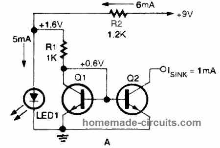
When a typical red LED is biased at 5 mA, the voltage drop across the diode reaches 1.6 volts. Because the base-emitter voltage of Q1 is approximately 0.6 volts, 1 volt is seen across R1.
The output current is proportional to the voltage at the base of the emitter. The output current reduces by a decade with every 60 mV reduction in voltage. The output current must be close to 10 microamps when R2 is set to drop 120 mV at 10 microamps.
LED1 and Q1 have identical temperature coefficients that subtract from R1's voltage drop; hence, excellent compensation may be achieved. The reference current is easily determined by dividing the value of R1 by one volt. The circuit has the extra benefit of allowing considerably lower values for R1 to be employed. This is highly beneficial in situations when low output current values are required.
Widlar Current Mirror
R1 values would typically be fairly high. Thankfully, there is another way to produce extremely low currents while keeping R1 within a tolerable range. The circuit indicated below is known as a Widlar current mirror.
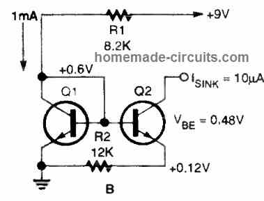
Additional resistor, R2, may be seen in Q2's emitter circuit. Assume the reference current is adjusted to 1 mA and R1 is fixed at 8200 ohms, and you want an output current of 10 microamps. Without R2, R1 would require a value of 820,000 ohms to accomplish this. By adding R2, however, we may lower the base-emitter voltage supplied to Q2.
Try a value of 12,000 ohms for R2 on the breadboard. With significantly lower resistor values, you might achieve an output near to 10 microamps.
Also, examine the output across its compliance range to see whether the accuracy has increased. The output impedance of the Widlar mirror is greater.
To decrease output resistance and bias issues, some designs employ an additional transistor to provide the base-current drive for Q1 and Q2.
The extreme speeds possible with current generators are demonstrated in our concluding current mirror example. Discrete BJT based current sources or sinks provide a significant benefit over op-amp-based solutions in certain cases.
Gating a Current Mirror
The next figure below illustrates how simple it is to "gate" a current mirror. R1 is driven directly through any conventional CMOS gate capable of handling the reference current. The CMOS gate controls the rise and fall timings.
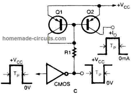
The circuit employs a 2N5117 transistor as an integrator, which is powered by an op-amp and gated at high speed. The current mirror, as you can see, is a very flexible circuit that could be categorized as a "Möbius" circuit. If you examine the relevance of the base-emitter voltage, it appears to have a singularity. Why not include it into your upcoming project?
3 Transistor Current Mirror is the Best
Referring to the figure shown below: if the current gain of the transistors (beta) is 100, the base currents are going to be 1% of the collector currents. If we consider that both the base currents to be '1', both the collector currents will be '100'. This subsequently implies that I1 = 102 and I2 = 100, that's a 2% error.
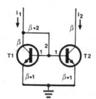
Naturally, the above error can be minimized by increasing the gain of the transistors. This implies that to build a most accurate current mirror circuit, the gain of the transistors will need to be at the infinite level.
However, an alternative improved method would be to introduce a third transistor to the circuit, as depicted in the next figure below.
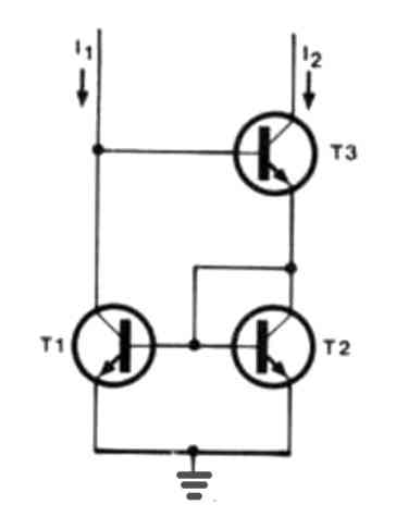
This helps to cut down the error by a factor which may be equivalent to the gain of the third transistor.
At the first glance this 3 transistor current mirror may look like as if it is built in the reverse order, with I2 being the input current, but in reality this is not the case.
Let us imagine that a current I1 is dumped down from the left side of the circuit, if T1 gets disabled in the process, the current would need to pass through T3 and down via T2.
T1 and T2 effectively create a current mirror: T1 will therefore pull a current equivalent to T2's collector current. This, in essence, is nearly equivalent to T3's collector current. Let's have a glance at the base currents now. Because all transistors are configured to almost equal collector currents, their base currents would be the same as well.
The emitter of T3 generates two base currents (for T1 and T2), 50% of which should match to the base current of T3 (that originates from I1 and the other 1/2 from I2). This indicates that I1 and I2 are extremely similar: the only distinction is that T3 requires a little greater base current so that the marginally higher collector current can flow. As previously indicated, this slight error is proportional to T3's current gain.
This three-transistor current mirror is practically perfect and without any flaws. It's worth noting that T2 is actually coupled as a 'diode.' Uncomfortable issues like temperature fluctuations, for example, have no negative impact if all three transistors are installed over a single common chip.
Dear Swagatam,
This a great article introducing intuition with current mirrors and the practical consideration for discrete BJT designs. I appreciate the article a lot as it has helped me understand how to look at discrete circuit design in terms of matching and temperature considerations.
sincerely,
Rauf
Thank you Dear Rauf, I am glad you found the post helpful. Please keep up the good work.
Good afternoon, sir Swagatam I don’t quite understand how this works, could you please explain to me with practical examples how it should be used in a circuit. Thank you very much.
Hi Carlos, you can see the “ideal current source” example where a current mirror circuit works to produce a constant current to the connected LED.
hi
i want to know about simulation of folded cascode current mirror
Sorry, I do not have it at this time, wll try to find it if possible