
The Field-Effect Transistor or the FET is a 3 terminal semiconductor device which is used for switching high power DC loads through negligible power inputs.
The FET comes with some unique features such as a high input impedance (in the megohms) and with almost zero loading on a signal source or the attached preceding stage.
The FET exhibits a high level of transconductance (1000 to 12,000 microohms, dependent on the brand and the manufacturer specs) and maximum operating frequency similarly is large (up to 500 MHz for quite a few variants).
I have already discussed the FET working and characteristic in one of my previous articles which you can go through for a detailed review of the device.
In this article I will elucidate some interesting and useful application circuits using field effect transistors. All these applications circuits presented below exploit the high input impedance characteristics of the FET for creating extremely accurate, sensitive, an wide range electronic circuits and projects.
FET Square wave Oscillator
Field effect transistors or FETs can be easily applied for making astable multivibrator (AMV) circuits. The output from the AMV from the FET configuration is a square wave which includes an amplitude of almost equal to the power supply voltage, and features a low battery drain. This FET square wave generator circuit can be operated with a battery supply of 9V.
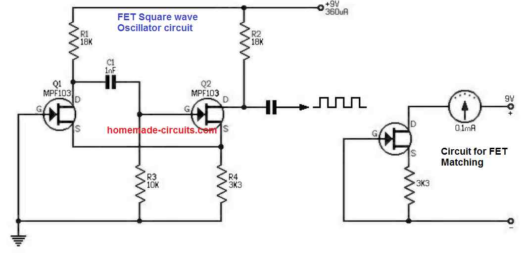
The Drain current consumption is quite low at around 360µA. The waveform exhibits an extremely good symmetry which is normally achieved by matching the FETs through the circuit shown on the left hand side. The FETs must be matched based on their equivalent drain currents. The operating frequency is determined by the values of the resistor R3 and the capacitor C1. The values as shown in the diagram would produce a frequency of approximately 15kHz.
Audio Preamplifier
FETs work very nicely for making mini AF amplifiers because it is small, it offers high input impedance, it demands just a tiny amount of DC power, and it offers great frequency response.
FET based AF amplifiers, featuring simple circuits, deliver excellent voltage gain and could be constructed small enough to be accommodated within a mic handle or in an AF test-probe.
These are often introduced into different products between stages in which a transmission boost is required and where prevailing circuitry should not be substantially loaded.
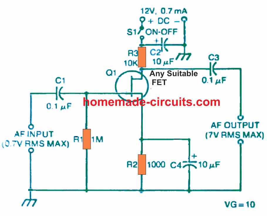
Figure above exhibits the circuit of a single-stage, one-transistor amplifier featuring the many benefits of the FET. The design is a common-source mode which is comparable with and a common-emitter BJT circuit.
The amp's input impedance is around the 1M introduced by resistor R1. The indicated FET is a low-cost and easily available device.
Voltage gain of the amplifier is 10. The optimum input-signal amplitude just before output-signal peak clipping is around 0.7 volt rms, and the equivalent output-voltage amplitude is 7 volt rms. At 100 % working specs, the circuit pulls 0.7 mA through the 12-volt DC supply.
Using a single FET the input-signal voltage, output-signal voltage and DC operating current could vary to some extent across the values provided above.
At frequencies between 100 Hz and 25 kHz, the amplifier response is within 1 dB of the 1000 Hz reference. All resistors can be 1/4 watt type. Capacitors C2 and C4 are 35-volt electrolytic packages, and capacitors C1 and C3 could be just about any standard low-voltage devices.
A standard battery supply or any suitable DC power supply works extremely; the FET amplifier can also be solar driven by a couple of series attached silicon solar modules.
If desirable, constantly adjustable gain control could be implemented by replacing a 1-megohm potentiometer for resistor R1. This circuit would nicely work as a preamplifier or as a main amplifier in a lot of applications demanding a 20 dB signal boost through the entire music range.
The increased input impedance and moderate output impedance will probably meet the majority of specifications. For extremely low-noise applications, the indicated FET could be substituted with standard matching FET.
2-stage FET amplifier circuit
The next diagram below exhibits the circuit of a two-stage FET amplifier which involves a couple of similar RC-coupled stages, similar what was discussed in the above segment.
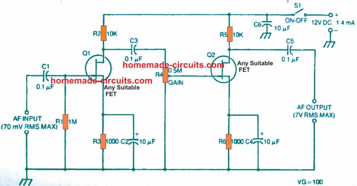
This FET circuit is designed to provide a large boost (40 dB) to any modest AF signal, and could be applied both individually or introduced as a stage in equipment requiring this capability.
The input impedance of the 2-stage FET amplifier circuit is around 1 megohm, determined by the input resistor value R1. All round voltage gain of the design is 100, although this number might deviate relatively up or down-with specific FETs.
The highest input-signal amplitude prior to output-signal peak clipping is 70 mV rms which results in the output-signal amplitude of 7 volts rms.
Under full functional mode, the circuit might consume roughly 1.4 mA through the 12-volt DC source, however this current could change a bit depending on the characteristics of specific FETs.
We did not find any need for including a decoupling filter across stages, since this type of filter could cause a reduction in the current of one stage. The unit's frequency response was tested flat within ± 1 dB of the 1 kHz level, from 100 Hz to better than 20 kHz.
Because the input stage extends “wide open,’’ there could be a possibility of hum pick up hum, unless this stage and the input terminals are properly shielded.
In persistent situations, R1 could be decreased to 0.47 Meg. In situations where amplifier needs to create smaller loading of the signal source, R1 could be increased to very large values up to 22 megohms, given the input stage shielded extremely well.
Having said that, resistance above this value might cause the resistance value to become same as the FET junction resistance value.
Untuned Crystal Oscillator
A Pierce-type crystal oscillator circuit, employing a single field-effect transistor, is shown in the following diagram. A Pierce-type crystal oscillator features the benefit of working without a tuning. It just needs to be attached with a crystal, then powered with a DC supply, to extract an RF output.
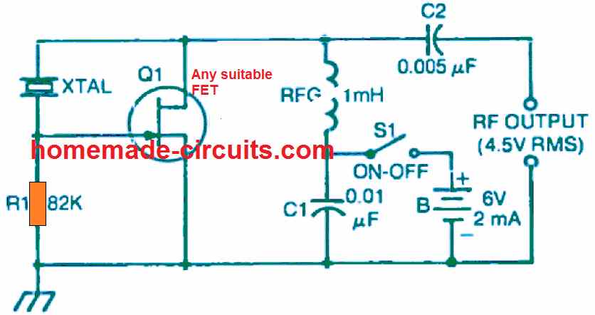
The untuned crystal oscillator is applied in transmitters, clock generators, crystal testers receiver front ends, markers, RF signal generators, signal spotters (secondary frequency standards), and several related systems. The FET circuit will show a quick start tendency for crystals that are beter suited for the tuning.
The FET untuned oscillator circuit consumes roughly 2 mA from the 6-volt DC source. With this source voltage, the open-circuit RF Output voltage is around 4% volts rms DC supply voltages as much as 12 volts could be applied, with correspondingly increased RF output.
To find out if the oscillator is functioning, shut switch S1 and hook up an RF voltmeter across the RF Output terminals. In case an RF meter is not accessible, you can use any high-resistance DC voltmeter appropriately shunted through a general-purpose germanium diode.
If the meter needle vibrates will indicate the working of the circuit and the RF emission. A different approach could be, to connect the oscillator with the Antenna and Ground terminals of a CW receiver that could be tuned with the crystal frequency in order to determine the RF oscillations.
To avoid flawed functioning, it is strongly recommended that the Pierce oscillator works with the specified frequency range of the crystal when the crystal is a fundamental-frequency cut.
If overtone crystals are employed, the output will not oscillate at the crystals rated frequency, rather with the lower frequency as decided by the crystal proportions. In order to run the crystal at the rated frequency of an overtone crystal, the oscillator needs to be of the tuned type.
Tuned Crystal Oscillator
Figure A below indicates the circuit of a basic crystal oscillator designed to function with most varieties of crystals. The circuit is tuned using screwdriver adjustable slug within inductor L1.
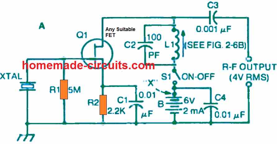
This oscillator can be easily customized for applications such as in communications, instrumentation, and control systems. It could even be applied as a flea-powered transmitter, for communications or RC model control.
As soon as the resonant circuit, L1-C1, is tuned to the crystal frequency, the oscillator starts pulling around 2 mA from the 6-volt DC source. The associated open-circuit RF output voltage is around 4 volts rms.
The drain current draw will be reduced with frequencies of 100 kHz compared to on other frequencies, because of the inductor resistance utilized for that frequency.
The next Figure (B) illustrates a list of industrial, slug-tuned inductors (L1) which work extremely well with this FET oscillator circuit.
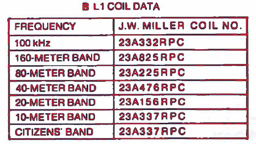
Inductances are selected for the 100 kHz normal frequency, 5 ham radio bands, and the 27 MHz citizens band; nevertheless, a considerable inductance range is taken care of by manipulation of the slug of each inductor, and a broader frequency range than the bands suggested in the table could be acquired with every single inductor.
The oscillator could be tuned to your crystal frequency simply by turning the slug up/down of the inductor (L1) to get optimum deviation of the connected RF voltmeter across the RF Output terminals.
Another method would be, to tune the L1 with a 0 - 5 DC hooked up at point X: Next, fine-tune the L1 slug until an aggressive dip is seen on meter reading.
The slug tuning facility gives you a precisely-tuned function. In applications in which it becomes essential to tune the oscillator frequently using a resettable calibration, a 100 pF adjustable capacitor should be used instead of C2, and the slug utilized just to fix the maximum frequency of the performance range.
Phase-shift Audio Oscillator
The phase-shift oscillator is actually a easy resistance-capacitance tuned circuit that is liked for its crystal clear output signal (minimum distortion sine wave signal).
The field-effect transistor FET is most favorable for this circuit, because the high input impedance of this FET produces almost no loading of the frequency-determining RC stage.
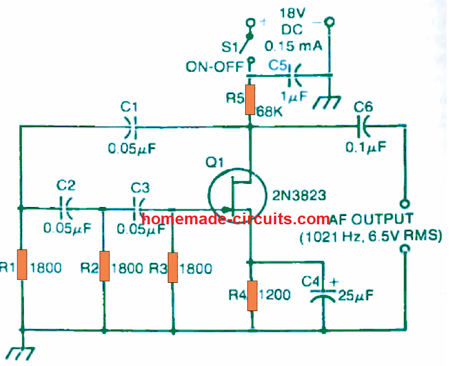
The figure above exhibits the circuit of a phase-shift AF oscillator working with a solitary FET. In this particular circuit, the frequency depends upon the 3-pin RC phase-shift circuit (C1-C2-C3-R1-R2-R3) which provides the oscillator its specific name.
For the intended 180° phase shift for oscillation, the values of Q1, R and C in the feedback line are appropriately chosen for generating a 60° shift on each individual pin (R1-C1, R2-C2. and R3-C3) between the drain and gate of FET Q1.
For convenience, the capacitances are selected to be equal in value (C1 = C2 = C3) and the resistances are likewise determined with equal values (R1 = R2 = R3).
The frequency of the network frequency (and for that matter the oscillation frequency of the design) in that case will be f = 1/(10.88 RC). where f is in hertz, R in ohms, and C in farads.
With the values presented in the circuit diagram, the frequency as a result is 1021 Hz (for precisely 1000 Hz with the 0.05 uF capacitors, R1, R2. and R3 individually should be 1838 ohms). While playing with a phase-shift oscillator, it might be better to tweak the resistors compared to the capacitors.
For an known capacitance (C), the corresponding resistance (R) to get a desired frequency (f) will be R = 1/(10.88 f C), where R is in ohms, f in hertz, and C in farads.
Therefore, with the 0.05 uF capacitors indicated in figure above, the resistance needed for 400 Hz = 1/(10.88 x 400 X 5 X 10^8 ) = 1/0.0002176 = 4596 ohms. The 2N3823 FET delivers the large transconductance (6500 /umho) necessary for optimum working of the FET phase-shift oscillator circuit.
The circuit pulls around 0.15 mA through the 18-volt DC source, and the open-circuit AF output is around 6.5 volts rms. All resistors used in the circuit are or1/4-watt 5% rated. Capacitors C5 and C6 could be any handy low voltage devices.
Electrolytic capacitor C4 is actually a 25-volt device. To ensure a stable frequency, capacitors Cl, C2, and C3 should be of best high quality and carefully matched up with capacitance.
Superregenerative Receiver
The next diagram reveals the circuit of a self-quenching form of superregenerative receiver constructed using a 2N3823 VHF field-effect transistor.
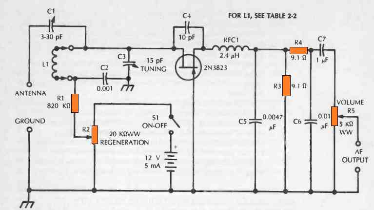
Using 4 different coils for L1, the circuit will quickly detect and start receiving the 2, 6, and 10-meter ham band signals and possibly even the 27 MHz spot. The coil details are indicated below:
- For receiving 10-meter band, or 27-MHZ band, use L1 = 3.3 uH to 6.5 uH inductance, over a Ceramic former, Powdered iron core slug.
- For receiving 6-meter band use L1 = 0.99 uH to 1.5 uH inductance, 0.04 over a Ceramic form, and iron slug.
- For receiving 2-Meter Amateur Band wind L1 with 4 turns No. 14 bare wire air-wound 1/2 inch diameter.
The frequency range enables the receiver specifically for standard communications as well as for radio model control. All inductors are solitary, 2-terminal packages.
The 27 MHz and 6 and 10-meter inductors are ordinary, slug-tuned units that needs to be installed on two-pin sockets for quick plug-in or replacing (for singleband receivers, these inductors could be soldered permanently over the PCB).
Having said that, the 2-meter coil has to be wound by the user, and also this should be furnished with a push-in type of base socket, apart from in a single-band receiver.
A filter network comprising (RFC1-C5-R3) eliminates the RF ingredient from the receiver output circuit, while an additional filter (R4-C6) attenuates the quench frequency. An appropriate 2.4 uH inductor for the RF filter.
How to Set Up
To check the superregenerative circuit in the beginning:
1- Connect high-impedance headsets to AF output slots.
2- Adjust the volume-control pot R5 to its highest output level.
3- Adjust regeneration control pot R2 to its lower most limit.
4- Adjust the tuning capacitor C3 to its highest capacitance level.
5- Press the switch S1.
6- Keep moving the potentiometer R2 until you find a loud hissing sound at one specific point on the pot, which indicates the start superregeneration. The volume of this hiss will be pretty consistent as you adjust the capacitor C3, however it should enhance a bit as R2 is moved up towards the uppermost level.
7-Next Hook up the antenna and the ground connections. If you find the antenna connection ceases hiss, fine-tune the antenna trimmer capacitor C1 until the hiss sound comes back. You will need to adjust this trimmer with an insulated screwdriver, only once to enable the range of all frequency bands.
8- Now, tune in signals in each and every station, observing the AGC activity of the receiver and the audio response of the speech processing.
9-The receiver tuning dial, mounted on C3 could be calibrated using an AM signal generator attached to the antenna and ground terminals.
Plug-in high-impedance earphones or AF voltmeter to AF output terminals, with each tweaking of the generator, adjust C3 for getting optimal level of audio peak.
The upper frequencies in the 10-meter, 6-meter, and 27 MHz bands could be positioned at the identical spot over the C3 calibration by altering the screw slugs within the associated coils, using the signal generator fixed at the matching frequency and having C3 fixed at the required point close to minimal capacitance.
The 2-meter coil, nevertheless, is without a slug and has to be tweaked by squeezing or stretching its winding for alignment with the top-band frequency.
The constructor should keep in mind that the superregenerative receiver is actually an aggressive radiator of RF energy and may severely conflict with other local receivers tuned in to the identical frequency.
The antenna coupling trimmer, C1, helps to provide a little bit of attenuation of this RF radiation and this might also result in a drop in the battery voltage to the minimum value which will nevertheless manage decent sensitivity and audio volume.
A radio-frequency amplifier powered in front of the superregenerator is a extremely productive medium for reducing RF emission.
Another simple Single FET regenerative radio circuit
Music Level Meter
C1 creates a buffer barrier between the level meter circuit and the audio signal input. VR1 is used for fine tuning the input signal to the gate of the FET, so this pot works like a sensitivity control.
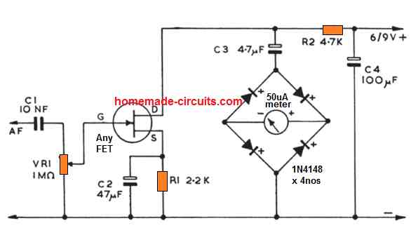
Audio power through the FET drain builds up a voltage around R2, and is connected to the full-wave rectifiers by C3. Current from this bridge rectifier configuration flows by means of the meter, to indicate an equivalent reading that is determined by the power of the fed audio signal.
This form of sensitive level meter or VU meter is advantageous for recording music through a calibrated scale that is supplied through VR1. It can be used likewise used to keep track of the level of audio signals commonly. The loading offered by the network of C1/VR1 is going to be of minimal significance for the majority of medium or reasonably low impedance circuits.
For apparent causes, AF obtained can be from a position right after any gain or volume controls in the sound products. The location where the signal amount is considerably excessive, a resistor could be positioned in series with C1. The value of this resistor relies on the signal voltage, however could be anticipated to lie between around 470k and 10 megohm
Electronic DC Voltmeter
The following figure displays the circuit of a symmetrical electronic DC voltmeter featuring an input resistance (which includes the 1-megohm resistor in the shielded probe) of 11 megohms.
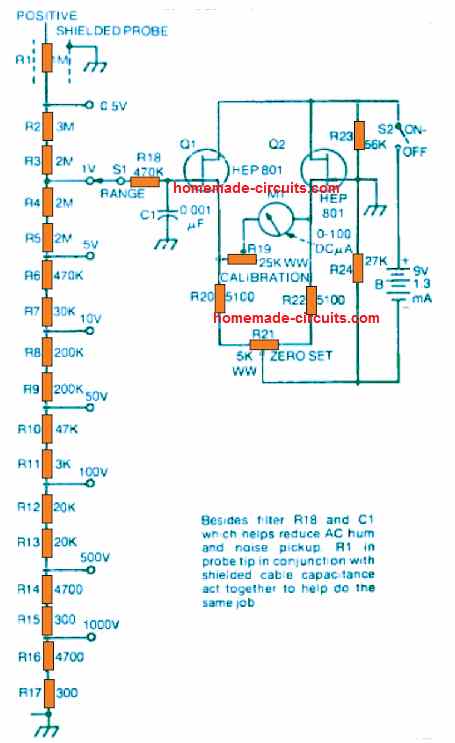
The unit consumes roughly 1.3 mA from a integrated 9-volt battery, B, thus could be left operational for long periods of time. This device specializes 0-1000 volts measurement in 8 ranges: 0-0.5, 0-1, 0-5, 0-10, 0-50, 0-100,0-500, andO-1000 volts.
The input voltage divider (range switching), the necessary resistances consist of series-connected stock-value resistors that needs to be determined cautiously for obtaining resistance values as close as possible to the portrayed values.
In case precision instrument-type resistors are obtainable, the quantity of resistors in this thread could be reduced by 50%. Meaning , for R2 and R3, replace 5 Meg.; for R4 and R5, 4 Meg.; for R6 and R7, 500 K; for R8 and R9, 400 K; for R10 and R11, 50 K; for R12 and R13, 40K; for R14 and R15, 5 K; and for R16 and R17,5 K.
This well balanced DC voltmeter circuit features almost no zero drift; any kind of drift in FET Q1 is countered automatically with a balancing drift in Q2. The internal drain-to-source connections of the FETs, along with resistors R20, R21, and R22, creates a resistance bridge.
Display microammeter M1 works like the detector within this bridge network. When a zero signal input is applied to the electronic voltmeter circuit, meter M1 is defined to zero by adjusting the balance of this bridge using potentiometer R21.
If a DC voltage hereafter is given to the input terminals, causes unbalancing in the bridge, due to the internal drain-to-source resistance alteration of the FETs, which results in a proportionate amount of deflection on the meter reading.
The RC filter created by R18 and C1 helps to eliminate AC hum and noise detected by the probe and the voltage-switching circuits.
Preliminary Calibration Tips
Applying zero voltage across the input terminals:
1 Switch ON S2 and adjust potentiometer R21 until the meter M1 reads zero on the scale. You can set the range switch S1 to any spot in this initial step.
2- Position range switch to its 1 V placement.
3- Hook up a precisely measured 1-volt DC supply across input terminals.
4- Fine-tune calibration control resistor R19 to get a precise full-scale deflection on meter M1.
5- Briefly take away the input voltage and check if the meter still remains at the zero spot. If you don't see it, reset R21.
6- Shuffle between the steps 3, 4, and 5 until you see full scale deflection on the meter in response to a 1 V input supply, and the needle returns to the zero mark as soon as 1 V input is removed.
Rheostat R19 will require no repeat setting up once the above procedures are implemented, unless of course its setting gets somehow displaced.
R21 which is meant for the Zero-setting may demand just infrequent resetting. In case range resistors R2 to R17 are precision resistors, this single-range calibration is going to be just enough; remaining ranges will automatically get into the calibration range.
An exclusive voltage dial could be sketched for the meter, or the already present 0 -100 uA scale could be marked in volts by imagining the appropriate multiplier across all except the 0 -100 volt range.
High Impedance Voltmeter
A voltmeter with a incredibly high impedance could be built through a field effect transistor amplifier. Figure below depicts a simple circuit for this function, that can be quickly customized into a further enhanced device.
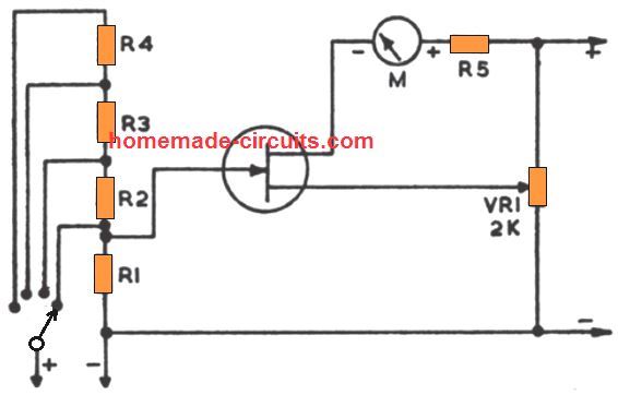
In the absence of a voltage input, R1 preserves the FET gate at negative potential, and VR1 is defined to ensure that supply current via the meter M is minimal. As soon as the FET gate is supplied with a positive voltage, meter M indicates the supply current.
Resistor R5 is only positioned like a current limiting resistor, in order to safeguard the meter.
If 1 megohm is used for R1, and 10 megohm resistors for R2, R3 and R4 will enable the meter to measure voltage ranges between roughly 0.5v to 15v.
The VR1 potentiometer can be normally 5k
The loading enforced by the meter on a 15v circuit is going to be a high impedance, more than 30 megohms.
Switch S1 is used for selecting various measuring ranges. If 100 uA meter is employed, then R5 could be 100 k.
The meter may not provide a linear scale, although specific calibration can be easily created through a pot and voltmeter, which enables the device all the desired voltages to be measured across the test leads.
Direct-reading Capacitance Meter
Measuring capacitance values quickly and effectively, is the main feature of the circuit presented in the circuit diagram below.
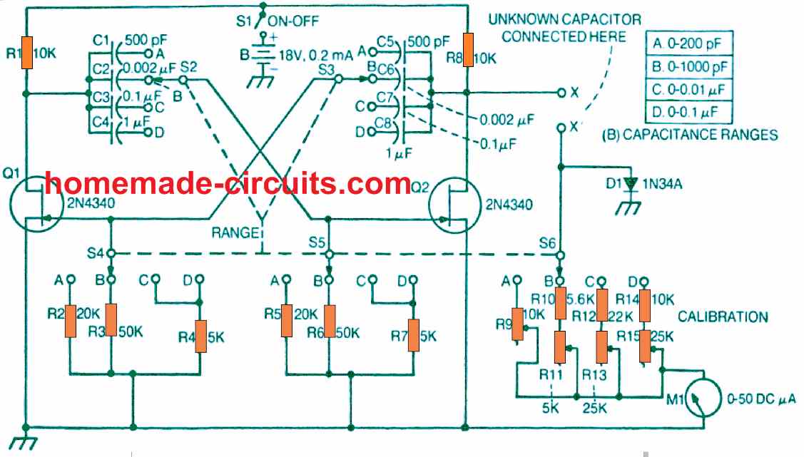
This capacitance meter implements this 4 separate ranges 0 to 0.1 uF 0 to 200 uF, 0 to 1000 uF, 0 to 0.01 uF, and 0 to 0.1 uF. Working procedure of the circuit is quite linear, which allows easy calibration of the 0 - 50 DC microammeter M1 scale in picofarads and microfarads.
An unknown capacitance plugged into slots X-X subsequently could be measured straight through the meter, without the need of any sort of calculations or balancing manipulations.
The circuit requires around 0.2 mA through an in-built 18-volt battery, B. In this particular capacitance meter circuit, the a couple of FETs (Q1 and Q2) are function in a standard drain-coupled multivibrator mode.
The multivibrator output, obtained from the Q2 drain, is a constant-amplitude square wave with a frequency mainly decided by the values of capacitors C1 to C8 and resistors R2 to R7.
The capacitances on each of the ranges are selected identically, while the very same is done for the resistances selection also.
A 6-pole. 4-position. rotary switch (S1-S2-S3-S4-S5-S6) picks the appropriate multivibrator capacitors and resistors along with the meter-circuit resistance combination necessary for delivering the test frequency for a selected capacitance range.
The square-wave is applied to the meter circuit through the unknown capacitor (connected across the terminals X-X). You don't have to worry about any zero meter setting; since the meter needle can eb expected to rest at the zero as long as an unknown capacitor is not plugged into slots X-X.
For a selected square-wave frequency, the meter needle deflection generates a directly proportional reading to the value of the unknown capacitance C, along with a nice and linear response.
Hence, if in the preliminary calibration of the circuit is implemented using a precisely identified 1000 pF capacitor attached to terminals X-X, and the range switch positioned to position B, and calibration pot R11 adjusted to achieve an exact full-scale deflection on the meter M1, then the meter will without any doubt measure the 1000 pF value at its full scale deflection.
Since the proposed capacitance meter circuit provide a linear response to its, the 500 pF can be expected to read at around half scale of the meter dial, 100 pF at 1/10 scale, and so forth.
For the 4 ranges of the capacitance measurement, the multivibrator frequency can be toggled to the following values: 50 kHz (0—200 pF), 5 kHz (0-1000 pF), 1000 Hz (0—0.01 uF), and 100 Hz (0-0.1 uF).
For this reason, switch segments S2 and S3 swap the multivibrator capacitors with equivalent sets in unison with switch sections S4 and S5 that switch the multivibrator resistors through equivalent pairs.
The frequency-determining capacitors should be capacitance-matched in pairs: C1 = C5. C2 = C6. C3 = C7, and C4 = C8. Similarly, the frequency-determining resistors should be resistance-matched in pairs: R2 = R5. R3 = R6, and R4 = R7.
The load resistors R1 and R8 at the FET drain likewise must be appropriately matched. The pots R9. R11, R13, and R15 that are used for the calibration should be wirewound types; and because these are adjusted only for the calibration purpose, they could be fitted inside the enclosure of the circuit, and furnished with slotted shafts for enabling adjustment through a screwdriver.
All the fixed resistors (R1 to R8. R10, R12. R14) should be 1-watt rated.
Initial Calibration
To begin the calibration process, you will need four perfectly known, very-low-leakage capacitors, having the values: 0.1 uF, 0.01 uF, 1000 pF, and 200 pF,
1-Keeping the range switch at position D, insert the the 0.1 uF capacitor to terminals X-X.
2-Switch ON S1.
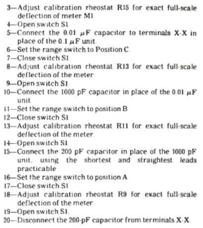
An distinctive meter card can be drawn, or numbers could be written on the existing microammeter background dial to indicate capacitance ranges of 0-200 pF, 0-1000 pF, 0-0.01 uF, and 0-0 1 uF.
As the capacitance meter is used further, you might feel it necessary to attach an unknown capacitor to terminals X-X turn ON S1 to test the capacitance reading on the meter. For greatest precision, it is advised to incorporate the range which will allow the deflection around the top section of the meter scale.
Field Strength Meter
The FET circuit below is designed to detect the strength of all frequencies within 250 MHz or may be even higher sometimes.
A small metal stick, rod, telescopic aerial detects and receives the radio frequency energy. The D1 rectifies the signals and supplies a positive voltage to the FET gate, over R1. This FET functions like a DC amplifier. The “Set Zero” pot could be any value between 1k to 10k.
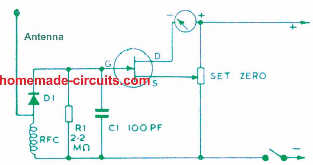
When no RF input signal is present, it adjusts gate/source potential in a way that the meter displays merely a tiny current, which increases proportionately depending on the level of the input RF signal.
To get higher sensitivity, a 100uA meter could be installed. Otherwise, a low sensitivity meter like 25uA, 500uA or 1mA might also work quite well, and provide the required RF strength measurements.
If the field strength meter is required to test for VHF only, a VHF choke will need to be incorporated, but for normal application around lower frequencies, a short wave choke is essential. An inductance of approximately 2.5mH is will do the job for up to 1.8 MHz and higher frequencies.
The FET field strength meter circuit could be built inside a compact metal box, with the antenna extended outside the enclosure, vertically.
While operating , the device enables tuning up a transmitter final amplifier and aerial circuits, or the realignment of bias, drive and other variables, to confirm optimum radiated output.
The result of adjustments could be witnessed through the sharp upward deflection or dipping of the meter needle or the reading on the field strength meter.
Moisture Detector
The sensitive FET circuit demonstrated below will recognize the existence of atmospheric moisture. As long as the sense pad is free of moisture, its resistance will be excessive.
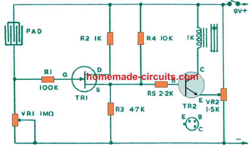
On the other hand the presence of moisture on the pad will lower its resistance, therefore TR1 will allow the conduction of current by means of P2, causing the base of TR2 to become positive. This action will activate the relay.
VR1 makes it possible for realignment of the level where TR1 switches ON, and therefore decides the sensitivity of the circuit. This could be fixed to an extremely high level.
The pot VR2 makes it possible for adjusting the collector current, to ensure that current through the relay coil is very small during the periods when the sensing pad is dry.
TR1 can be the 2N3819 or any other common FET, and TR2 can be a BC108 or some other high gain ordinary NPN transistor. The sense pad is quickly produced from 0.1 in or 0.15 in matrix perforated circuit PCB with conductive foil across the rows of holes.
A board measuring 1 x 3 inches is adequate if the circuit is used as a water level detector, however a more substantial sized board (maybe 3 x 4 inches) is recommended for enabling FET moisture detection, especially during rainy season.
The warning unit can be any desired device such as an indication light, bell, buzzer or sound oscillator, and these could be integrated inside the enclosure, or positioned externally and be hooked up through an extension cable.
Voltage Regulator
The simple FET voltage regulator I have explained below offers reasonably good efficiency using a least number of parts. The fundamental circuit is demonstrated below (top).
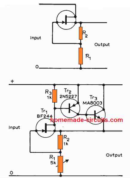
Any kind of variation in output voltage induced through an alteration in load resistance changes the gate-source voltage of the f.e.t. via R1, and R2. This leads to a counteracting change in drain current. The stabilization ratio is fantastic ( ≈ 1000) however the output resistance is quite high R0> 1/(YFs > 500Ω) and the output current is actually minimal.
To defeat these anomalies, the improved bottom voltage regulator circuit can be utilized. The output resistance is tremendously decreased without compromising the stabilization ratio.
The maximum output current is restricted by the permissible dissipation of the last transistor.
Resistor R3 is selected to create a quiescent current of a couple of mA in TR3. A good test set-up applying the values indicated, caused an alteration of less than 0.1 V even when the load current was varied from 0 to 60 mA at 5 V output. The impact of temperature on the output voltage was not looked into however it could possibly be kept under control through proper selection of the drain current of the f.e.t.
Audio Mixer
You may sometimes be interested to fade-in or fade-out or mix a couple of audio signals at customized levels. The circuit presented below can be used for accomplishing this purpose. One particular input is associated to socket 1, and the second to socket 2. Each one input is designed to accept high or other impedances, and possesses independent volume control VR1 and VR2.
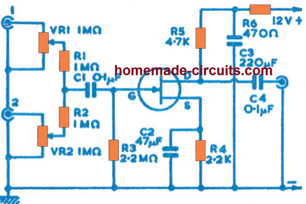
R1 and R2 resistors offer isolation from the pots VR1 and VR2 to ensure that a lowest setting from one of the pots doesn't ground the input signal for the other pot. Such a set up is appropriate for all standard applications, using microphones, pick-up, tuner, cellphone, etc.
The FET 2N3819 as well as other audio and general purpose FETs will work without any issues. Output must be a shielded connector, through C4.
Simple Tone Control
Variable music tone controls enable customization of audio and music as per personal preference, or allow certain magnitude of compensation to boost overall frequency response of an audio signal.
These are invaluable for standard equipment which is often combined with crystal or magnetic input units, or for radio and amplifier, etc., and which lack input circuits intended for such music specialization.
Three different passive tone control circuits are demonstrated in Figure below.
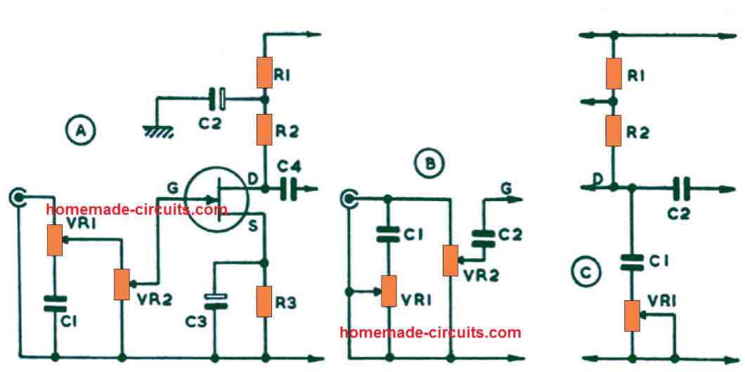
These designs can be made to work with a common preamplifier stage as shown in A. With these passive tone control modules there may be a general loss of audio causing some reduction in the output signal level.
In case the amplifier at A includes sufficient gain, satisfactory volume could still be achieved. This is dependent upon the amplifier as well as other conditions, and when it is assumed that a preamplifier might reestablish volume. In stage A, VR1 works like the tone control, higher frequencies is minimized in response to its wiper travelling towards C1.
VR2 is wired to form a gain or volume control. R3 and C3 offer source bias and by-passing, and R2 function as the drain audio load, while the output is acquired from C4. R1 with C2 are used for decoupling the positive supply line.
The circuits can be powered from a 12v DC supply. R1 could be modified if required for greater voltages. In this and related circuits you will find substantial latitude in the selection of magnitudes for positions such as C1.
At circuit B, VR1 works like a top cut control, and VR2 as the volume control. C2 is coupled to the gate at G, and a 2.2 M resistor offers the DC route through gate to negative line, remaining parts are R1, R2, P3, C2, C3 and C4 as at A.
Typical values for B are:
- C1 = 10nF
- VR1= 500k linear
- C2 = 0.47uF
- VR2 = 500k log
Another top cut control is revealed at C. Here, R1 and R2 are identical to R1 and R2 of A.
C2 of A being incorporated like at A. Occasionally this type of tone control could be included in a pre-existing stage with virtually no hindrance to the circuit board. C1 at C can be 47nF, and VR1 25k.
Larger magnitudes could be tried for VR1, however that could result in a large section of the audible range of VR1 consume just a little portion of its rotation. C1 could be made higher, to provide enhanced top cut. The results attained with different part values are affected by the impedance of the circuit.
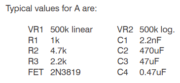
Single Diode FET Radio
The next FET circuit below shows a simple amplified diode radio receiver using a single FET and some passive parts. VC1 could be a typical size 500 pF or identical GANG tuning capacitor; or a small trimmer in case all proportions need to be compact.
The tuning antenna coil is built using fifty turns of 26 swg to 34 swg wire, over a ferrite rod. or could be salvaged from any existing medium wave receiver. The number of winding will enable the reception of all nearby MW bands.
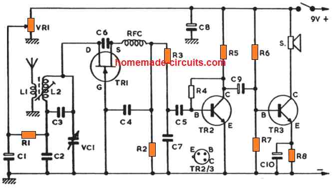
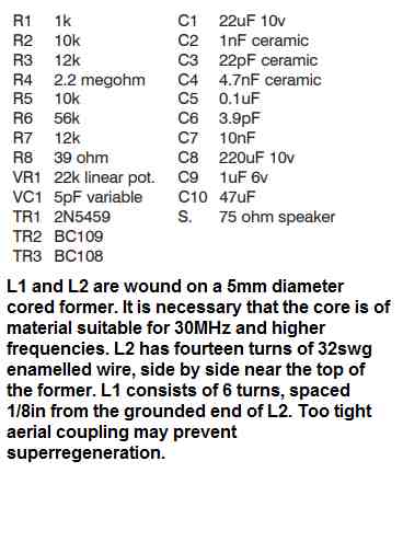
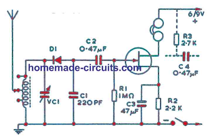
MW TRF Radio Receiver
The next relatively comprehensive TRF MW radio circuit can be built using just a coupe of FETs. It is designed to provide a decent headphone reception. For a longer range a longer antenna wire could be attached with the radio, or else it could be utilized with lower sensitivity by depending on the ferrite rod coil only for nearby MW signal pick-up. TR1 works like the detector, and regeneration is achieved through tapping on the tuning coil.
The application of regeneration significantly enhances selectivity, as well as sensitivity to weaker transmissions. The potentiometer VR1 permits manual realignment of the drain potential of TR1, and so functions as a regeneration control. Audio output from TR1 is connected with TR2 by C5.
This FET is an audio amplifier, driving the headphones. An full headset is more suitable for casual tuning in, although phones of approximately 500 ohms DC resistance, or around 2k impedance, will deliver excellent results for this FET MW radio. In case a mini earpiece is desired for the listening, this can be a moderate or high impedance magnetic device.
How to make the Antenna Coil
The tuning antenna coil is built using fifty turns of super enameled 26swg wire, over a standard ferrite rod having a length of around 5in x 3/8in. In case the turns are wrapped over a thin card pipe that facilitates sliding of the coil on the rod, might make it possible for adjusting of band coverage optimally.
The winding will start at A, the tapping for the antenna can be extracted at point B which is at around twenty-five turns.
Point D is the grounded end terminal of the coil. The most effective placement of the tapping C will depend fairly on the FET selected, the battery voltage, and whether the radio receiver will be combined with an external aerial wire without an antenna.
If the tapping C is too close to end D, then regeneration will cease to initiate, or will be extremely poor, even with VR1 turned for optimum voltage. However, having a lot many turns between C and D, will lead to oscillation, even with VR1 just a bit rotated, causing the signals to get weakened.
JFET Biasing Circuits
The JFET can be used in digital and also in linear circuits. When it is used in a low-distortion analog amplifier, the JFET should be controlled in its linear region by enabling a reverse biasing on its gate with respect to its source.
You will find three popular JFET biasing methods: self, offset, and constant-current.
JFET Self Biasing
Self-biasing can be witnessed in figure below.
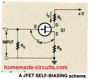
The JFET's gate can be seen grounded by means of resistor RG, and the source is grounded by the resistor Rs. Any current passing into Rs will cause the source to be positive relative to its gate, which means the gate will be perfectly reverse-biased.
In case drain current (ID) requires to be fixed at 1 milliampere, and we know that a minimum gate-to-source bias voltage (VGS) of -2.2 volts is necessary, the accurate value of source resistor (Rs) has to be established.
You can get the right bias through a 2k2 ohm resistor. Using Ohms law, we find that if a 2.2 V develops across the 2k2 resistor, will allow the flow of 1 mA current. When drain current drops, gate-to-source bias voltage also drops. Due to this the drain current increases, and balances the original difference.
Therefore, the JFET biasing can be self-regulating using a negative feedback. The gate-source bias necessary to establish a preferred drain current can differ extensively even between similar JFET's in real circuits. Hence, the only guaranteed method to fix an exact drain current would be to select a source resistor by experimentation or make use of a potentiometer.
No matter exactly how it is implemented, self-biasing works nicely for the majority of practical applications, and it uses just a couple of external parts for its working. That is why self-biasing method continues to be the most widely used method, to bias a JFET.
Offset Biasing
The second biasing technique is the offset biasing, which can be seen outlined in the figure below.
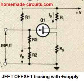
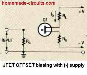
It provides a much more improved gate biasing compared to self-biasing. In this concept, the voltage at the R1 and R2 junction is employed like a fixed positive bias into the gate of the JFET, through a resistor RD. The voltage available at the source becomes same as this bias voltage minus the negative value of the gate-source bias.
As a result, if the positive gate voltage is big enough with regard to gate-source bias, drain current can be manipulated predominantly through Rs and gate-voltage. This may not be significantly affected by modifications of gate-source bias between specific JFET's. Offset biasing enables drain current to be established correctly, eliminating the need of selecting specific resistor for the operation. Comparable effects could be seen simply by grounding the gate and connecting the lower-end of the source resistor with a high negative voltage, as demonstrated in Fig. 5 -b.
Constant Current Biasing
The 3rd JFET basing idea, which is the constant-current biasing, can be seen below.
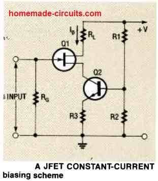
Here, the resistor at the source of the JFET is substituted by NPN bipolar transistor Q2, that is arranged like a constant-current source. As a result it ensures the supply for the drain current. The constant current is defined by Q2's base voltage, that is fixed through the resistors R1 and R2 voltage divider and emitter resistor R3.
Resistor R2 may likewise be changed with a Zener diode or some other voltage reference. Therefore, within this bias circuit, drain current is not dependent on the specifications of the JFET, which results in a great stability of the biasing of the device.
However, this specific enhancement is acquired at the cost of extra parts. In the 3 biasing schemes, resistor RG may have virtually any value approximately upto 10 M. This restriction is enforced due to the voltage drop over the resistor, caused by gate leakage currents, which could create problems for the biasing conditions of the device.
Source-Followers Circuits
JFET transistors when used in linear amplifiers are generally constructed with either a common-source or common-drain (source-follower) configuration. These configurations work like a JFET equivalents of the BJT common-emitter and common-collector (emitter-follower) amplifier, respectively. The source-follower configuration provides extremely high input impedance and close to unity total voltage gain. (For this reason it's additionally known as voltage follower).
A straightforward source-follower amplifier can be visualized in figure below.
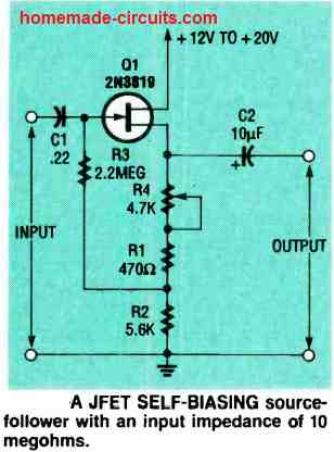
It is a self-biasing type, and drain current could be adjusted through a potentiometer R4. This self-biasing source-follower amplifier works using any voltage ranging from +12 to +20 volt supply. Potentiometer R4 must be adjusted to ensure the quiescent voltage around R2 is 5.6 volts, that supplies a 1 milliampere drain current. This set up can provide a voltage gain of approximately 0.95 across input and output.
Due to the voltage division on the intersection of potentiometer R4, the series R1 resistor and resistor R2, a little of bootstrapping develops at R3.
In this configuration, in which the output is obtained from the emitter of the JFET, the output voltage specifically influences the biasing of the device. In this amplifier, negative output pulses result in a rise in the negative voltage at the input, and positive output leads to a lowering of the negative voltage at the input.
The input is connected between the source and the gate of the JFET. The bootstrapping in this network increases the net value of R3 with a factor of approximately 5. The design's input impedance is approximately 10 megohms, shunted by the 10 picofarads capacitor. Consequently, input impedance could be as large as 10 megohms when the frequencies are minimal. Nevertheless, the value of the resistor may reduce to around 1 megohm with frequencies at 16 kHz, and may still be lowered to approximately 100 K at 160 kHz.
The next figure below, is another form of source-follower amplifier which includes offset biasing. Resistor manipulation is not really required for this amplifier, and its net voltage gain is approximately 0.95. Electrolytic capacitor C2, which gives bootstrapping, increases the effective R3 gate resistor value to around 20 times.

Having said that, this isn't necessary for the normal functioning of the amplifier. Having C2 removed from the amplifier, the source-follower's input impedance becomes 2.2 megohms, shunted by 10 picofarads. Having C2 in position, input impedance is enhanced to about 44 megohms, likewise shunted by 10 picofarads. Some other impedance values might be acquired by increasing R3 up to an optimum value of 10 megohms.
MORE FET CIRCUITS CAN BE DOWNLOADED FROM THE FOLLOWING LINK:
https://www.homemade-circuits.com/wp-content/uploads/2021/05/FET-circuits_removed.pdf