Electronic signals have been quite successfully sent for decades through standard "hard -wire" connections, or by using radio links of different kinds which had many disadvantages.
On the other hand fiber optic links, whether used for audio or video links over long ranges, or to handle small distances, have been offering some distinct advantages compared to the normal wired cables.
How Fiber Optic Works
In fiber optic circuit technology an optical fiber link is used for transferring digital or analogue data in the form light frequency through a cable which has a highly reflective central core.
Internally, the optical fiber consists of a highly reflective central core, which acts like a light guide for transferring light through it by means of continuous to and fro reflections across its reflective walls.
The optical link normally includes an electrical frequency to light frequency converter circuit, which converts digital or audio signals into light frequency. This light frequency is "injected" to one of the ends of the optical fiber through a powerful LED. The light is then allowed to travel through the optical cable to the intended destination, where it is received by a photocell and an amplifier circuit which converts the light frequency back to the original digital form or audio frequency form.
Advantages of Fiber Optics
One major advantage of fibre optic circuit links is their perfect immunity to electrical interference and stray pick ups.
Standard "cable" links could be designed to reduce this problem, however it may be a lot challenging to completely eradicate this issue.
On the contrary, the nonelectrical characteristics of a fiber optic cable helps make electrical interference immaterial, apart from some disturbance that could be picked at the receiver end, but this can be also eliminated through an effective shielding of the receiver circuit.
Quite similarly, broadband signals routed across a regular electrical cable often dissipate electrical disturbance causing jamming of radio and television signals close by.
But again, in case of a fiber optic cable it truly can prove to be entirely devoid of electrical emissions, and even though transmitter unit may possibly crank out some radio frequency radiation, it is rather simple to enclose it utilizing basic screening strategies.
Due to this plus point, systems incorporating many optic cables working together one beside another have no complications or issues with cross-talks.
Of course light could possibly leak out from one cable to the next, but fiber optic cables are usually encapsulated in an light proof external sleeving which ideally prevents any form of light leakage.
This strong shielding in fibre optic links ensures a reasonably safe and reliable data transfer.
Another advantage is that fiber optics are free from fire hazard problems since no electricity or high current flow in involved.
We also have a good electrical isolation throughout the link to ensure that complications with earth loops are unable to develop. Through appropriate transmitting and receiving circuits it becomes well suited for fiber optic links to handle substantial bandwidth ranges.
Wide bandwith links could be created through coaxial power cables also, although modern optic cables typically experience reduced losses compared to coaxial types in wide bandwidth applications.
Optic cables are typically slim and lightweight, and also immune to climatic conditions and several chemical substances. This frequently allows them to be applied quickly in inhospitable surroundings or unfavorable scenarios where electrical cables, specifically coaxial types simply turn out to be very ineffective.
Disadvantages
Although fiber optics circuit have so many advantages these have a few down sides also.
The apparent disadvantage is that electrical signals cannot be transferred directly into an optical cable, and in several situations the cost and problems encountered with the vital encoder and decoder circuits tend to get quite incompatible.
A crucial thing to remember while working with optical fibers is that they ordinarily have a specified least diameter, and when these are twisted with a sharper curve gives rise to physical damages to the cable at that bend, making it useless.
The "minimum bend" radius as it is normally called in the datasheets, is typically between approximately 50 and 80 millimetres.
The consequence of such bends in a normal wired mains cable could be just nothing, however for a fiber optic cables even small tight bends can hinder the propagation of the light signals leading to drastic losses.
Basic of Fiber Optics
Though it may seem to us that a fiber optic cable simply is made up of glass filament covered within an light proof external sleeving, the situation are in fact a lot more advanced than this.
Nowadays, the glass filament is mostly in the form of a polymer and not actual glass, and the standard set up may be as laid out in the following Figure. Here we can see a central core having a high refractive index and an outer shielding with reduced refractive index.

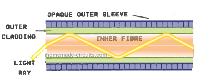
Refraction where the inner filament and the outer cladding interact makes it possible for light traverse through the cable by efficiently jumping across wall to wall all the way through the cable.
It is this bouncing of the light across the cable walls that makes it possible for the cable to run like a light guide, carrying the illumination smoothly about corners and the curves.
High Order Mode Light Propagation
The angle at which the light is reflected is determined by the properties of the cable and the input angle of the light. In the above Figure the light ray can be seen put through a "high order mode" propagation.
Low Order Mode Light Propagation
However, you will find cables with light fed with a shallower angle causing it to bounce between cable walls with a considerably wide angle. This lower angle allows the light to travel at relatively greater distance through the cable on each bounce.
This form of light transfer is termed "low order mode" propagation. The practical significance of both of these modes is that light venturing via the cable in the high order mode needs to travel appreciably further as compared to light that is propagated in the low order mode. This smudges signals delivered down the cable reducing the the frequency range of the application.
However, this is only relevant in extremely wide bandwidth links.
Single Mode Cable
We also have the "Single mode" type cables which are intended simply for enabling a single propagation mode, but it is not really required to utilize a this form of cable with the comparatively narrow bandwidth techniques detailed in this article. You may further come across an alternate kind of cable named "graded index" cable.
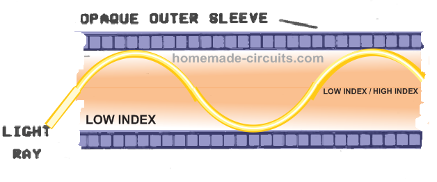
This is in fact pretty similar to the stepped index cable discussed earlier, although there exists a progressive transformation from a high refractive index near the center of the cable to a reduced value near to the outer sleeving.
This causes the light passing deep across the cable in quite similar manner as explained earlier, but with the light having to go through a curved route (as in the following Figure) instead of being propagated through straight lines.
Optic Fiber Dimensions
The typical dimension for optical fiber cables is 2.2 millimetres with an average dimension of the inner fiber being around 1 millimetre. You can find several connectors accessible for connections across this size of cable, in addition to a number of systems that hook up to equally matching cables.
A normal connector system includes a "plug" that is installed onto the tip of the cable and safeguards it to the "socket" terminal which usually brackets over the circuit board having a slot for accommodating the photocell (which forms the emitter or the detector of the optical system).
Factors Affecting Fiber Optic Circuit Design
One crucial aspect that needs to be remembered in fiber optics is the peak output specifications of the emitter photocell for the light wavelength. This must be ideally selected to match the transmission frequency with appropriate sensitivity.
The second factor to remember is that the cable will be specified with only a limited bandwidth range, which means the losses must be as minimum as possible.
The optical sensors and transmitters normally used in optical fibers are mostly rated to work at the infrared range with utmost efficiency, while some may be intended to work best with the visible light spectrum.
Fibre optic cabling are frequently delivered with unfinished terminating ends, which could be very unproductive, unless the ends are appropriately trimmed and worked.
Typically, the cable will provide decent effects when it is sliced at right angles with a razor-sharp modelling knife, chopping the cable end cleanly in one action.
A fine file may be used to polish the sliced ends, but if you've only just cut the ends, this may not help to significantly enhance the light efficiency. It is crucial that cut is sharp, crisp and perpendicular to the cable diameter.
If the cutting has some angle may severely deteriorate the efficiency due to deviation in angle of the light feed.
Designing a Simple Fiber Optic System
A basic way to start for anyone looking to try things out with fiber optic communications would be to create an audio link.
In its most elementary form this may include a simple amplitude modulation circuitry which varies the LED transmitter brightness in accordance with the amplitude of the audio input signal.
This would cause an equivalently modulating current response across the photocell receiver, which would be processed to genearte a correspondingly varying voltage across a calculated load resistor in series with the photocell.
This signal would be amplified to deliver the audio output signal. In reality this fundamental approach may come with its own downsides, the major one may be simply an insufficient linearity from the photocells.
Absence of linearity affects in the form of a proportionate level of distortion across the optical link that may be subsequently of bad quality.
A method that normally offers significantly better outcomes is a frequency modulation system, which is basically identical to the system used in standard VHF radio broadcasts.
However, in such cases a carrier frequency of around 100 kHz is involved instead of the conventional 100 MHz as used in band 2 radio transmission.
This approach can be pretty simple, as shown in the block diagram below. It demonstrates the principle set up for a one way link of this form. The transmitter is actually a voltage controlled oscillator (VCO), and as the title suggests, the output frequency from this design could be adjusted through a control voltage.
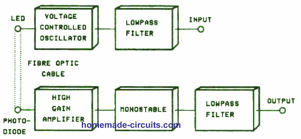
This voltage may be the sound input transmission, and as the signal voltage oscillates up and down, so will the VCO's output frequency. A lowpass filter is incorporated to refine the audio input signal before it is applied to the VCO.
This helps to keep the heterodyne "whistles" away from being produced on account of beat notes between the voltage controlled oscillator and any high frequency input signals.
Typically, the input signal is only going to cover the audio frequency range, but you may find distortion content at higher frequencies, and radio signals getting picked up from the wiring and interacting with the VCO signal or harmonics around the VCO's output signal.
The emitting device which may be simply an LED is driven by the VCO output. For optimal result this LED is normally a high wattage type of LED. This necessitates the use of a driver buffer stage for operating the LED power.
This next stage is a monostable multivibrator which must be designed as a non-retriggerable type.
This enables the stage to generate output pulses through intervals as determined by the C/R timing network which is independent of the input pulse duration.
Operational Waveform
This provides an easy yet effective frequency to voltage conversion, having waveform as depicted in the following figure clearly explains its operational pattern.
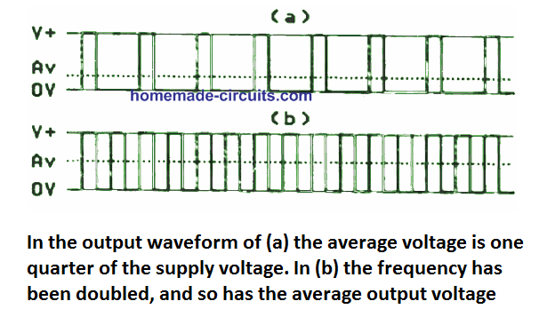
In Figure (a) the input frequency generates an output from the monostable with a 1 to 3 mark-space ratio, and the output is in the high state for 25% of the time.
The average output voltage (as depicted inside the dotted line) is as a result 1/4 of the output HIGH state.
In Figure (b) above we can see that the input frequency has been increased by two fold, which means we get two times more output pulses for a specified time interval with a mark space ratio of 1:1. This allows us to get an average output voltage that is 50% of HIGH output state, and 2 times more magnitude of the previous example.
In simple terms, the monostable not only helps to convert frequency to voltage, but it additionally enables the conversion to get a linear characteristic. The output from the monostable alone cannot build an audio frequency signal, unless a lowpass filter is incorporated which ensures that the output is stabilized into a proper audio signal.
The primary problem with this simple method of frequency to voltage conversion is that a higher level attenuation (essentially 80 dB or higher) is required at the minimum output frequency of the VCO to be able to create a stabilized output.
But, this method is really simple and dependable in other considerations, and together with modern circuits it may not be difficult to design an output filter stage having a appropriately precise cut off characteristic.
A tiny level of surplus carrier signal on the output may not be a too critical and could be ignored, because the carrier is generally at frequencies which is not within the the audio range, and any leakage at the output will as a result be inaudible.
Fiber Optic Transmitter Circuit
The entire fiber optic transmitter circuit diagram can be seen below. You will find many integrated circuits suitable to work like VCO, along with many other configurations built using discrete parts.
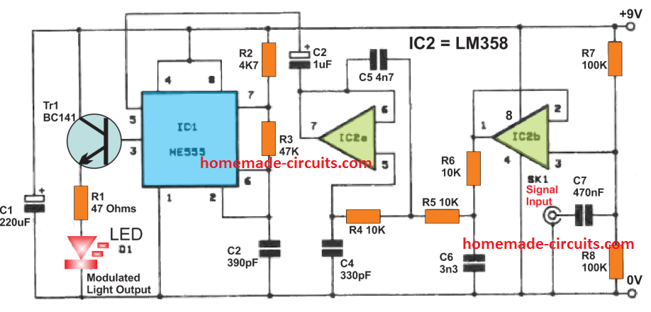
But for a low cost technique the widely used NE555 becomes the preferred option, and though it certainly cheap, yet comes with a fairly good performance efficiency. It may be frequency modulated by integrating the input signal to pin 5 of the IC, that connects with the voltage divider configured to create the 1/3 V+ and 2/3 V+ switching limits for the IC 555.
Essentially, the upper limit is increased and decreased so that the time consumed for the timing capacitor C2 to switch between the two ranges could be correspondingly increased or decreased.
Tr1 is wired like an emitter follower buffer stage which supplies the high drive current required for illuminating the LED (D1) optimally. Although the NE555 itself features a good 200 mA current for the LED, a separate current controlled driver for the LED allows to establish the desired LED current in a precise way and through a more reliable method.
R1 is positioned to fix the LED current at approximately 40 milliamps, but since the LED is switched ON/OFF at a rate of 50% duty cycle allows the LED to work with only 50% of the actually rating which is about 20 milliamps.
The output current could be increased or decreased by adjusting the R1 value whenever this may be felt necessary.
Components for Fiber Optic Transmitter Resistors (all 1/4 watt, 5%)
R1 = 47R
R2 = 4k7
R3 = 47k
R4 = 10k
R5 = 10k
R6 = 10k
R7 = 100k
R8 = 100k
Capacitors
C1 = 220µ 10V elect
C2 = 390pF ceramic plate
C3 = 1u 63V elect
C4 = 330p ceramic plate
C5 = 4n7 polyester layer
C6 = 3n3 polyester layer
C7 = 470n polyester layer
Semiconductors
IC1 = NE555
IC2 = 1458C
Tr1 = BC141
D1 = see text
Miscellaneous
SK1 3.5mm jack socket
Circuit board, case, battery, etc
Fiber Optic Receiver Circuit
The primary fiber optic receiver circuit diagram can be seen in the upper section of the below diagram, the output filter circuit is drawn just below the receiver circuit. The output of the receiver can be seen joined with the input of the filter through a grey line.
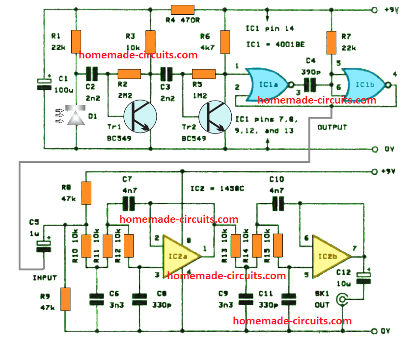
D1 forms the detector diode, and it works in the reverse bias setting in which its leakage resistance helps to create a kind of light dependent resistor or LDR effect.
R1 works like a load resistor, and C2 creates a link between the detector stage and the input amplifier input. This forms a two-stage capacitively linked network where the two stages function together in the common emitter mode.
This allows a superior overall voltage gain greater than 80 dB. given that a fairly powerful input signal is supplied, this offers an adequately high output voltage oscillation at the Tr2 collector pin to push the monostable multivibrator.
The latter is a standard CMOS type built using a couple of 2-input NOR gates (IC1a and IC1b) with C4 and R7 functioning like timing elements. The other a couple of gates of IC1 are not used, although their inputs can be seen hooked to earth in an effort to stop false switching of these gates due to stray pick up.
Referring to filter stage built around IC2a/b, it is fundamentally a 2/3rd order (18 dB per octave) filter systems with specifications commonly employed in the transmitter circuits. These are joined in series to establish a total of 6 poles and a general attenuation rate of 36 dB per octave.
This offers approximately 100 dB of attenuation of the carrier signal in its minimum frequency range, and an output signal with a relatively low carrier signal levels. The Fiber Optic Circuit can deal with input voltages as high as 1 volt RMS approximately with no critical distortion, and help to work with marginally less than unity voltage gain for the system.
Components for Fibre Optic Receiver and Filter
Resistors (all 1/4 watt 5%)
R1 = 22k
R2 = 2M2
R3 = 10k
R4 = 470R
R5 = 1M2
R6 = 4k7
R7 = 22k
R8 = 47k
R9 = 47k
R10 to R15 10k (6 off)
Capacitors
C1 = 100µ10V electrolytic
C2 = 2n2 polyester
C3 = 2n2 polyester
C4 = 390p ceramic
C5 = 1µ 63V electrolytic
C6 = 3n3 polyester
C7 = 4n7 polyester
C8 = 330pF ceramic
C9 = 3n3 polyester
C10 = 4n7 polyester
Semiconductors
IC1 = 4001BE
1C2 = 1458C
IC3 = CA3140E
Trl , Tr2 BC549 (2 off)
D1 = See text
Miscellaneous
SK1 = 25 way D connector
Case, circuit board, wire, etc.
my professor tells me that my graduation project is this circuit do you sure that this circuit works
If you a newcomer in the field of electronics then this project is not for you. This project is recommended only for the experts. This project will work but only if done 100% correctly. and also the user should know how to troubleshoot a fault if there’s any mistake in the connections or the parts.
how to simulate this circuit and how to make the channel effect
Sorry, I am not sure about how it can be done.
my professor tells me that my graduation project is this circuit do you sure that this circuit work
This is a wonderfully straightforward circuit. Can it be adapted to create a full-duplex, USB 2.0 transceiver (i.e., extender)?
Hello Bhushan, are you looking for a light to music converter circuit?
You can refer to the following article:
How to make simple a LI-FI (Light Fidelity) Circuit
Good afternoon, Swagatam!
I saw your circuit and I really liked its didactics.
I would like to make an optical / coaxial fiber converter. The receiving party would look the same, right? What changes is the filter part? How would it be ? Thank you for your attention.
Thank you Lucas, there’s no change required in the filter stage, you can use exactly the same filter stage for your purpose also…..
Dear Sir: I have a interruoter for a tesla coil built after a project from Steve Wards. The connection to the coil driver was not designed to be fiber optic, but I want to do this. I have the transmitter which is with 850 nm led, maximum 2.2 V and Imax = 100 mA. The switch has three NE555 and offers a rectangular signal with a cycle of ~ 19% with a frequency in the range of 100-800 Hz and a variable pulse width. Can your circuit be used for my purpose?
Dear Bocanet, I am not an expert in fiber optic technology so I won’t be able to answer your question, instead you can read the above article thoroughly and judge yourself whether your assumption is feasible or not.
I don’t think you understood me. I want to understand your circuit. I simulated it on the Circuit Wizard and it seems to work, but when I modeled it on the breadboard, I had my signal (800 Hz) at the output of the op-amp, at the output of 555 a rectangular signal 30 Khz and at the LED terminals also a 30 KHz signal. I don’t understand how the modulation is done and why don’t I have a signal similar to the input signal at the output? Audio signals are analog signals with variable amplitude and frequency. I have a signal with the same amplitude, rectangular, with a frequency, at a time constant but which can be changed between 100 and 800 Hz and with the same variable bandwidth. Does the transistor work as a switch or in the linear amplification zone?
Sincerely, Corneliu Bocanet
The op amp input is supposed to have an analogue audio signal so that it is converted into corresponding PWM digital signal by yhe IC 555. In this PWM signal the pulse width is supposed to vary in accordance with the amplitude of the analogue audio. If you are applying a constant amplitude 800 Hz, that won’t have any affect on the IC 555 output and the output will continue to deliver a constant frequency PWM based on the values of R2, R3, C2. The transistor works only like a switch!