The field-effect transistor (FET) is an electronic device in which an electric field is used to regulate the flow of current. To implement this a potential difference is applied across the gate and source terminals of the device, which alters the conductivity between the drain and source terminals causing a controlled current to flow across these terminals.
FETs are called unipolar transistors because these are designed to operate as single-carrier-type devices. You will find different types of field effect transistors available.
Symbol
The graphical symbols for the n-channel and p-channel JFETs can be visualized in the following figures.
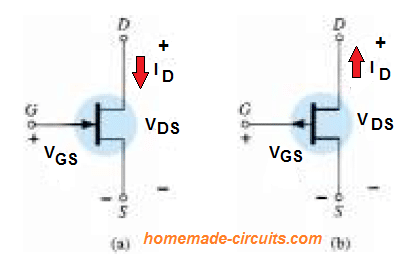
You can clearly notice that the arrow marks which are pointing inward for the n-channel device to indicate the direction in which IG (gate current) is supposed to flow when the p-n junction were forward-biased.
In case of a p-channel device the conditions are identical except the difference in the direction of the arrow symbol.
Difference between FET and BJT
The field-effect transistor (FET) is a three-terminal device designed for a wide range of circuit applications that complement, to a great level, those of the BJT transistor.
While you will find significant variances between BJTs and JFETs, there are actually several matching characteristics which will be talked about in the following discussions. The main distinction between these devices is BJT is a current-controlled device as represented in Fig. 5.1a, while the JFET transistor is a voltage-controlled device as indicated in Fig. 5.1b.
Put simply, the current IC in Fig. 5.1a is an immediate function of the level of IB. For the FET the current I is a function of the voltage VGS given to the input circuit as demonstrated in Fig. 5.1b.
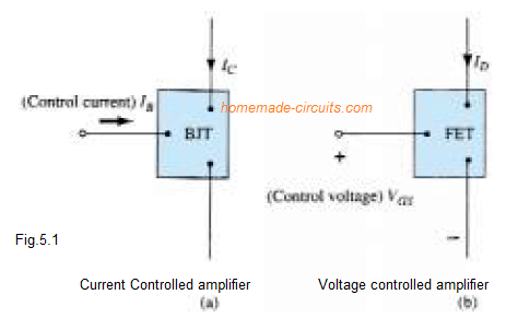
In both the instances the current of the output circuit will be governed by a parameter of the input circuit. In one situation a current level and in the other an applied voltage.
Just like npn and pnp for bipolar transistors, you will find n-channel and p-channel field-effect transistors. But, you should remember that the BJT transistor is a bipolar device the prefix bi- indicating that the conduction level is a function of two charge carriers, electrons and holes.
The FET on the other hand is a unipolar device that solely depends on either electron (n-channel) or hole (p-channel) conduction.
The phrase "field-effect" can be explained like this: all of us are aware of the power of a permanent magnet to attract metal filings towards the magnet without any physical contact. Quite in a similar way inside FET an electric field is created by the existing charges that influence the conduction path of the output circuit without having any direct contact between the controlling and controlled quantities. Probably one of the most crucial features of the FET is its high input impedance.
Ranging from a magnitude of 1 to many hundred megohms it significantly surpasses the normal input resistance ranges of the BJT configurations, an extremely important attribute while developing linear ac amplifier models.
However, the BJT carries a greater sensitivity to variations in the input signal. Meaning, the change in output current is commonly significantly more for BJTs than FETs for the same amount of change in their input voltages.
Because of this, standard ac voltage gains for BJT amplifiers can be a much higher compared to FETs.
Generally speaking, FETs are considerably more thermally resilient than BJTs, and also are often smaller sized in structure compared to BJTs, which make them specifically suitable for embedding as integrated-circuit (IC) chips.
The structural characteristics of some FETs, on the other hand, can allow them to be extra sensitive to physical contacts than BJTs.
More BJT/JFET Relationship
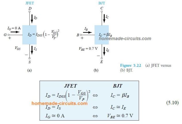
- For a BJT VBE = 0.7 V is the important factor for starting an analysis of its configuration.
- Similarly, the parameter IG = 0 A is commonly the first thing considered for the analysis of a JFET circuit.
- For the BJT configuration, IB is often the first factor that becomes necessary to be determined.
- Likewise, for the JFET, it is typically the VGS.
In this article we will be focussing on JFETs or junction field effect transistors, in the next article we'll dicuss about metal-oxide-semiconductor field-effcet transistor or MOS-FET.
CONSTRUCTION AND CHARACTERISTICS OF JFETs
As I have explained earliet a JFET has 3 leads. One of them controls the current flow between the other two.
Just like BJTs, in JFETs too the n-channel device is used more prominently than the p-channel counterparts, since n devices tend to more efficient and user friendly compared to the p-device.
In the following figure we can see the basic structure or construction of a n-channel JFET. We can see that the n-type composition forms the principal channel across the p-type layers.
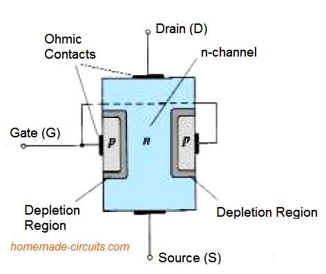
The upper part of the n-type channel is joined through an Ohmic contact with a termnal named the drain (D), while the lower section of the same channel also connected through a Ohmic contact with another terminal named the source (S).
The couple of p-type materials are together linked with the terminal referred to as the gate (G). Essentially we find that the drain and source terminals are joined to the ends of the n-type channel. The gate terminal is joined to a pair of p-channel material.
When there's no voltage applied across a jfet, its two p-n junctions are without any biasing conditions. In this situation there exists a depletion region on each junction as indicated in the above figure, which looks quite like a diode p-n region under no biasing.
Water Analogy
The working and control operations of a JFET can be understood through the following water analogy.
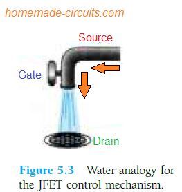
Here, the water pressure can be compared with the applied voltage magnitude from drain towards source.
The flow of water can be compared with the flow of electrons. The mouth of the tap imitates the source terminal of the JFET, while the upper portion of the tap where the water is forced in depicts the Drain of the JFET.
The tap knob acts like the Gate of the JFET. With the help of an input potential it controls the flow of electrons (charge) from drain to source, just as the tap knob controls the flow of water on the mouth opening.
From the JFET structure we can see that the drain and the source terminals are at the opposite ends of the n-channel, and as the term is based of electron flow we can write:
VGS = 0 V, VDS Some Positive Value
In the Fig 5.4 we can see a positive voltage VDS applied across the n-channel. The gate terminal is directly joined to the source to create a condition VGS = 0V. This enables the gate and the source terminals to be at an identical potential, and results in a lower end depletion region of each p-material, exactly as we see in the first diagram above with a no-bias condition.
As soon as a voltage VDD ( = VDS) is applied, electrons are pulled towards the drain terminal, generating the conventional flow of current ID, as indicated in Fig 5.4.
The direction of the flow of the charge reveals that the drain and source current are equal in magnitude (ID = IS). As per the conditions depicted in the Fig 5.4, the flow of the charge looks quite unrestricted, and only affected by the resistance of the n-channel between drain and the source.
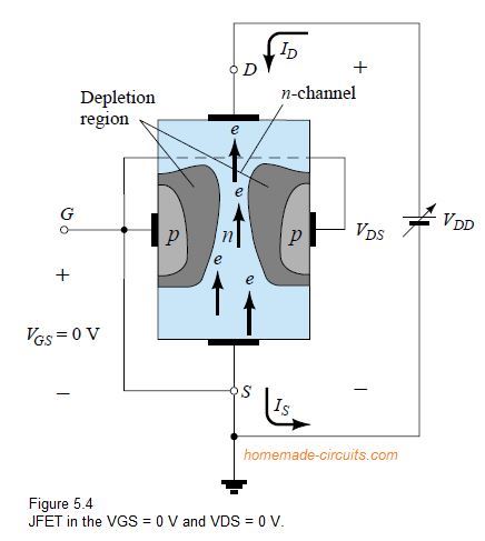
You may observe that the depletion region is bigger around the top section of both p-type materials. This difference in size of the region is ideally explained through the Fig. 5.5. Let's imagine having a uniform resistance in the n-channel, this could be split up to the sections indicated in Fig. 5.5.
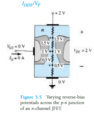
The current ID may build the voltage ranges through the channel as pointed out in the same figure. As a result the upper region of the p-type material is going to be reverse biased by a level of around 1.5 V, with the lower region being merely reverse-biased by 0.5 V.
The point that the p-n junction is reverse-biased along the entire channel gives rise to a gate current with zero amperes as displayed in the same figure. This characteristic which leads to IG = 0 A is an important characteristic of the JFET.
As VDS potential is increased from 0 to a some volts, the current increases as per Ohm’s law and the plot of ID versus VDS can look as proven in Fig. 5.6.
The comparative straightness of the plotting shows that for the low value regions of VDS, the resistance is basically uniform. As VDS rises and nears a level known as VP in Fig. 5.6, the depletion regions widens as given in Fig 5.4.
This results in a apparent lowering of the channel width. The decreased conduction path leads to the increase in resistance giving rise to the curve of Fig. 5.6.
The more horizontal the curve gets, the higher is the resistance, indicating that the resistance is getting towards “infinite” ohms in the horizontal region. When VDS increases to an extent where it would appear that the two depletion regions might “contact” as displayed in Fig. 5.7, gives rise to a situation known as pinch-off.
The amount by which VDS develops this situation is called the pinch-off voltage and it is symbolized by VP as presented in Fig. 5.6. In general, the word pinch-off is misleading because it implies the current ID is "pinched off" and falls to 0 A. As proven in Fig. 5.6, this hardly looks evident in this case. ID retains a saturation level characterized as IDSS in Fig. 5.6.
The truth is a very little channel continues to exist, with a current of significantly high concentration.
The point that ID does not drop off at pinch-off and preserves the saturation level as indicated in Fig. 5.6 is confirmed with the following proof:
Since there's no drain current eliminates the possibility of diverse potential levels through the n-channel material for determining the changing amounts of reverse bias along the p-n junction. The end result being loss of the depletion region distribution that triggered pinch-off to start with.

As we increase VDS above VP, the close contact region where the two depletion regions will encounter with each other increase in length along the channel. However the ID level continues to be essentially unchanged.
Thus the moment VDS is higher than Vp, the JFET acquires the characteristics of current source.
As proven in Fig 5.8 current in a JFET is determined at ID = IDSS, but voltage VDS higher than VP is established by the connected load.
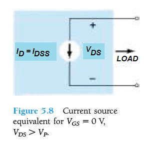
The selection of IDSS notation is based on the fact that it is the Drain to Source current having a short circuited link across gate to source.
Further investigation gives us the following evaluation:
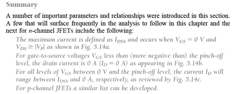
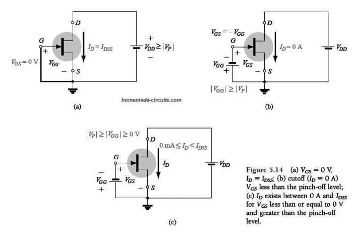
IDSS is the highest drain current for a JFET and is established by the conditions VGS = 0 V and VDS > |VP|.
Notice that in Fig. 5.6 VGS is 0V for the complete stretch of the curve. In the following sections I have explained how the Fig 5.6 attributes become influenced as the level of VGS is varied.
VGS < 0V
The volatage applied across the gate and source is signified as the VGS, which is responsible for controlling the JFET operations.
If we take the example of a BJT, just as the curves of IC vs VCE are determined for various levels of IB, similarly the curves of ID vs VDS for various levels of VGS can be created for a JFET counterpart.
For this the gate terminal is set at a continued lower potential below the level of the source potential.
Referring to the Fig.5.9 below, a -1V is applied across the gate/source terminals for a reduced VDS level.
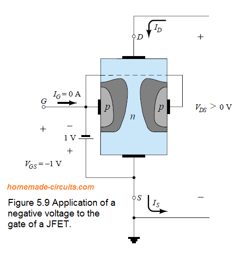
The objective of negative potential bias VGS is to develop depletion regions resembling the situation of VGS = 0, but at significantly reduced VDS.
This causes the gate to attain a saturation point with a lower levels of VDS as indicated in Fig. 5.10 (VGS = -1V).
The corresponding saturatio level for ID can be found to be reduced and actually just goes on decreasing as VGS is made more negative.
You can clearly see in Fig. 5.10 how the pinch-off voltage carries on dropping with a parabolic shape as VGS gets more and more negative.
Finally, when VGS = -Vp, it gets sufficiently negative to establish a saturation level which is eventually 0 mA. At this level, the JFET is completely "turned OFF".
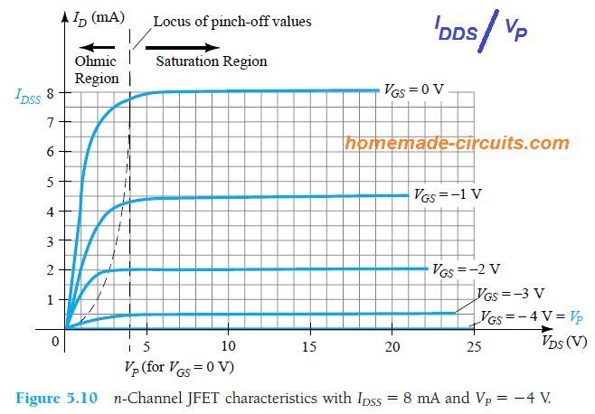
The level of VGS which causes ID to reach 0 mA is characterized by VGS = VP, wherein VP is a negative voltage for n-channel devices and a positive voltage for p-channel JFETs.
Commonly, you may find most JFET datasheets showing pinch-off voltage specified as VGS(off) instead of VP.
The area at the right hand side of the pinch-off locus in the above figure is the place conventionally used in linear amplifiers for achieving distortion free signal. This region is generally called constant-current, saturation or linear amplification region.
Voltage-controlled Resistor
The area which is on the left side of the pinch-off locus in the same figure, is called the ohmic region or the voltage-controlled resistance region.
In this region the device can be in fact operated as a variable resistor (for example in automatic gain control application), with its resistance controlled through the applied gate/source potential.
You can see that the slope of each of the curves which also signifies the drain/source resistance of the JFET for VDS < VP happens to be a function of the applied VGS potential.
As we make VGS higher with negative potential, the slope of each curve gets more and more horizontal, exhibiting proportionately increasing resistance levels.
We are able to get a good initial approximation to the level of the resistance with respect to the VGS voltage, through the following equation.

p-Channel JFET Working
The internal layout and construction of a p-channel JFET is precisely identical to the n-channel counterpart, except that the p- and n-type materials regions are reversed, as shown below:
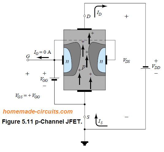
The directions of the current flow can be also seen as reversed, along with the actual polarities of voltage VGS and VDS. In case of a p-channel JFET, the channel will get constrained in response to increasing positive potential across the gate/source .
The notation with a double subscript for the VDS will give rise to negative voltage for VDS, as shown on the characteristics of Fig.5.12. Here, you can find IDSS at 6 mA, while a pinch-off voltage at VGS = +6V.
Please do not get puzzled due to the presence of thee minus sign for the VDS. It simply indicates that source carries a higher potential than the drain.
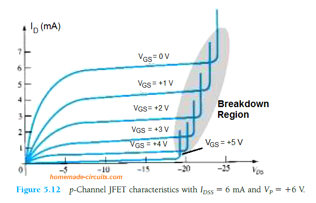
You can see that the curves for high VDS levels abruptly rise to values that look unrestricted. The indicated rise which are vertical symbolize a breakdown situation, which means the current through the channel device is entirely controlled by the external circuitry at this point of time.
Although this is not apparent in Fig.5.10 for n-channel device, it may be a possibility under sufficiently high voltage.
This region can be eliminated if the VDS(max) is noted from the datasheet of the device, and the device is configured such that the actual VDS value is lower than this noted value for any VGS.
