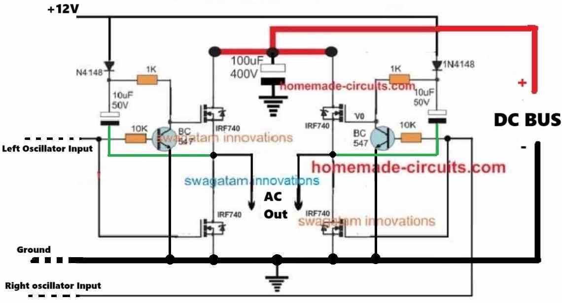
In this article I will elucidate a simple universal H-bridge module using BJTs and N-channel MOSFETs.
This module can be integrated with any standard oscillator ICs such as IC 4047 or IC SG3525 or even IC 555, to create a highly efficient H-bridge inverter circuits.
Why using 4 N-channel MOSFET H-Bridge is the Most Efficient
Using 4 N--channel MOSFETs in an H-bridge configuration is considered to be the most efficient topology because N-channel MOSFETs have much lower RDSon compared to their P-channel counterparts.
Lower RDSon means lower drain to source resistance, which ensures lower heat dissipation and higher current transfer across the MOSFETs.
The Challenge behind 4 N-Channel MOSFET H-Bridge
However creating a H-bridge using N-channel MOSFETs can be difficult since it involves a relatively complex a bootstrapping network.
The bootstrapping network refers to a small circuit network around the gates of the high-side MOSFETs which enables the high-side MOSFETs to conduct freely by ensuring that its gate voltage is always around 12V higher than its instantaneous source voltage.
Now, let's try to understand how our universal H-bridge circuit module using N-channel MOSFETs works.
How the Circuit Works
If you don't want to read the following description, you can watch this video instead:
Referring to the diagram below, let's assume an instantaneous moment where the left side oscillator input is low, and the right side oscillator input is high.

In this situation, the left side BC547 is turned OFF due to the absence of the base switching voltage, and the left side 10uF/50V capacitor is charged up to the battery voltage level through the 1N4148 diode.
Now, the left high-side MOSFET gets its voltage through the 1N4148 diode, and the 1k resistor, and makes an attempt to conduct.
However, as soon as the MOSFET drain voltage reaches its source terminal and exceeds its gate voltage (12V), the conduction stalls, because as we know, ideally, for any MOSFET to conduct, its gate potential must be around 10V higher than its source potential.
This is where our BC547 and 10uF bootstrapping network comes into action.
When the Left high-side MOSFET drain voltage reaches the source terminal, this voltage is forced into the 10uF capacitor through its negative terminal.
This source voltage entering the negative terminal of the 10uF capacitor now comes in series with the existing 12V stored inside the 10uF capacitor.
So, as the source voltage rises it pushes the stored potential inside the 10uF higher so that the total voltage at the gate of the MOSFET is always 12V higher than the source voltage of the MOSFET.
So, when the source voltage is 12V, it adds up with the internal 12V of the 10uF capacitor producing 12 + 12V = 24V at the gate of the high side MOOSFET.
This means the effective gate voltage is now the difference between the total gate voltage and the source voltage, that is 24V minus 12V = 12V, or if suppose the drain supply is 100 volts, then the effective gate voltage will be 100 volts plus 12 volts minus 100 volts = 12 Volts
This ensures that the gate voltage of the high side MOSFET is always held at 12V higher than its source voltage.
This in turn enable the high side N channel MOSFETs to conduct freely and efficiently, regardless of the applied drain voltage level. This may not be possible if P-channel MOSFETs are used, although P-channel MOSFET wouldn't require a bootstrapping.
A High-side P-channel MOSFET might not require a bootstrapping, but the main disadvantage of using P-channel high-side MOSFETs is, its drain voltage cannot exceed the gate voltage, which simply means that if the oscillator IC output is 12V, then the load voltage cannot exceed 12V, which appears to be a big drawback, which is completely eliminated if N-channel MOSFETs are used.
That's it! this concludes our tutorial on a simple H-bridge circuit module using N-channel MOSFETs which can be used to transform any center tapped inverter into an H-bridge inverter.
I hope you liked the tutorial…. for any further doubts or queries, please feel free to comment below for quick replies.
Summary
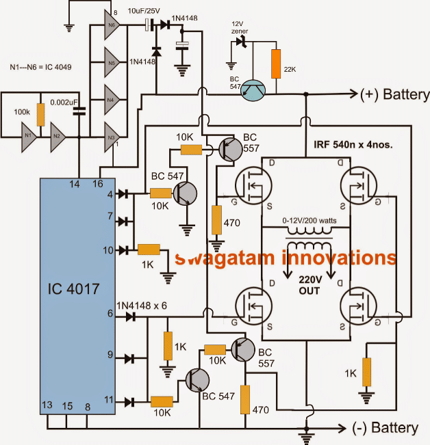
The H-bridge inverter topology is the most efficient one, since it does not necessitate the use of center tap transformers, and allows the use of transformers with two wires. The results become even better when four N-channel mosfets are involved.
With a two wire transformer connected to an H-bridge means the associated winding is allowed to go through the push pull oscillations in a reverse forward manner. This provides better efficiency as the attainable current gain here becomes higher than the ordinary center tap type topologies.
However better things are never easy to get or implement. When identical type mosfets are involved in an H-bridge network, driving them efficiently becomes a big problem. It is primarily due to the following facts:
As we know an H-bridge topology incorporates four mosfets for the specified operations. With all four of them being N-channel types, driving the upper mosfets or the high side mosfets becomes an issue.
This is because during conduction the upper mosfets experience almost the same level of potential at their source terminal as the supply voltage, due to the presence of the load resistance at the source terminal.
That means the upper mosfets come across similar voltage levels at their gate and source while operating.
Since as per the specs, the source voltage must be close to the ground potential for efficient conduction, the situation instantly inhibits the particular mosfet from conducting, and the entire circuit stalls.
In order to switch the upper mosfets efficiently they must be applied with a gate voltage at least 6V higher than the available supply voltage.
Meaning if the supply voltage is 12V, we would require at least 18-20V at the gate of the high side mosfets.

